Note: Descriptions are shown in the official language in which they were submitted.
CA 02015162 2000-08-O1
METHOD OF AND APPARATUS FOR INCREASING THE PROCESSING
SPEED~IN THE SCANNING INSPECTION OF CIRCUIT BOARDS AND
OTHER OBJECTS
The present invention relates to image-scanning in-
spection systems, such as used in the detection of faults
or defects in printed circuit bards and other objects,
being more particularly directed to systems of the type
described, for example, in my earlier U.S. Letters Patent
No. 4,589,140, and other inspection systems, as well, and
to the improvement in increasing the effective processing
speed of operations thereof.
As described in said Letters Patent, for example,
techniques are successfully used to scan at rapid speeds
printed circuit boards or other surfaces and to monitor
the detection of defects, irregularities or other features
in the boards that deviate from known or accepted fea-
tures. Included in such prior systems are the Circuit One*
apparatus of Beltronics, Inc. of Brookline, Massachusetts,
assignee of the present invention, which operates in
accordance with the methodology and apparatus disclosed in
said above-entitled Letters Patent.
* Trade-Mark
CA 02015162 2000-08-O1
-2-
There are occasions, however, where it is desired to
increase the throughput speed of inspection; and the pre-
sent invention is directed to achieving such through a
novel pre-processing method or technique that, while pa~-
ticularly adapted for inspection systems of the above-
described type, are more generally applicable to other
types or philosophies of sr_anning inspection, as well.
An object of the invention, accordingly, is to pro-
vide a new and improved method of and apparatus for the
inspection of defects, irregularities or other features in
surfaces and in which increased speed of throughput is
attained by novel pixel pre-processing techniques.
Other and further objects will be explained herein-
after and are more particularly pointed out in connection
with the appended claims.
Brief Description of the Drawings
The invention will now be described with reference
to the accompanying drawings, Fib. 1 of which is a diagra-
matic view of a large pixel composed of small camera
pixels for use in accordance with the method underlying
the invention;
~01~16,
-3-
Figs. 2A and 2B are binary representations of an
array of pixels representing the optical scanning detec-
tion, respectively, of exemplary pinhole and speck de-
fects:
Figs. 2C and 2D are diagrams similar to Fig. 1 of the
sets of larger pixels of the invention for the respective
cases of Figs. 2A and 2B;
Figs. 3A and 3B correspond to the cases of Figs. 2C
and 2D, respectively, with appropriate binary value
assignments resulting from majority neighborhood value
determination;
Figs: 4A and 4B correspond, respectively, to the cir-
cumstances of Figs. 3A and 38, illustrating camera timing
and line assignments;
Fig. 5 is similar to Figs. 4A and 4B illustrating
two-camera interleaving;
Fig. 6 is a block circuit diagram of a preferred pre-
processor operating in accordance with the invention;
Fig. 7 is a similar diagram of a circuit for majority
value determination and assignment and including broader
~ol~~sz
-4-
region majority value determination as shown in Fig. 7A;
ana
Fibs. $ and 9 are block and flow diagrams of a pre-
(erred implame~tation of the systems o!' Fi~s. 6 and 7.
In summary, from one of its broader aspects, the in-
vention embraces a method of increasing the processing
speed of optical scanning in which an object is scanned by
a camera to determine defects, features. or differences,
that comprises, scanning the objects to generate binary
value small pixels corresponding to the presence or ab-
sence of physical characteristics; generating from the
small pixels a set of larger pixels each constitutes of a
group of the small pixels; conveying to the larger pixels
defect, feature or difference information contained in one
or more of the small pixels constituting the same; and
processing the larger pixels at a data rate or processing
speed that is a multiple of that achievable in processing
the small pixels, while maintaining the information from
the scanning that is contained in the small pixels. Pre-
(erred and best mode embodiments and details will later be
presented.
. ; , . ...
205162
-5-
Considering the illustration of circuit board inspec-
tion as an example, current high-speed inspection systems
of the above-described and related types must be designed
to detect very small defects, such as hairline breaks,
hairline shorts, pinholes, specks and critical minute
errors. To do so, very small picture elements must be
chosen, referred to as pixels, that are sufficiently small
to enable the detection of such small defects. Unfortun-
ately, however, when pixel size is very small, and the
objects such as the circuit boards are large, there are a
very large number of pixels to process. To reduce such ,
large numbers of pixels, and thus enhance the processing
speed, the present invention provides a scheme whereby
larger pixels are generated (actually groups of smaller
pixels). Inspection is made of the information within the
group of smaller pixels to determine whether the same
contains a defect or region of difference from its
surrounding pixels; and, if so, this information is
conveyed to the larger pixel. Thus, the number of pixels .
is reduced by converting the small pixels into larger
201~~.62
pixels or pixel groups, and the data rate is accordingly
reduced while still maintaining the information contained
in the small pi:cels through conveying such information tn
the large pixel group.
Camera pixels P, Fig. 1, have binary values of 1 or 0
to denote the presence or absence of conducting material
or other physical characteristics or features. The larger
pixel P1 (shown composed of four camera pixels P), like
the camera pixel P, has also a binary value of 1 or 0; but
the binary value is computed in such a way as to accentu-
ate in the large pixel P1 small defects or variations, so
that they are detected by the shape-recognition algorithm,
as of said Letters Patent, which will then process the
larger pixels. .
This process will now be explained with the aid of
Figs. 2A and 2B which respectively show a pinhole in a
printed circuit line (indicated by a 0) and a speck in the
board laminate (indicated as a 1). To compute the value
of a large pixel P1 one examines the neighborhood of at
least an array of six-by-six camera pixels P which is
CA 02015162 2000-08-O1
equivalent to at least a set of three-by-three large
pixels P1 Fig. 2C. The value of the neighborhood is said
to be the majority value of the camera pixels surrounding
the center four camera pixels. For example, ~aith the
pinhole, Fig. ZA, the majority equals a 1; and for the
speck, Fig. 2D, the majority equals 0. The number of
pixels that differ from the majority value are computed.
The value of the center large pixel P~1~ Figs. 2C and
2D, is then set equal to the opposite value of the
neighborhood if a certain or some minimum number T of the
pixels in the center group differ from the neighborhood to
accentuate the pixel that is different. Otherwise, it is
set equal to the same value as the neighborhood. Thus, for
the pinhole of Fig. 2C, the large pixels P1 will have the
values shown in Fig. 3A, where the center larger pixel Pcl
is 0 because of the 0 information within the center larger
pixel of Fig. 2C. Similarly, the center pixel Pcl of
Fig. 3B, for the case of the speck in the laminate,
reflects by its 1 value, the information within the cen-
ter large pixel Pcl of Fig. 2D.
201516
_8_
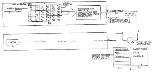
Relative to camera timing, the large pixels P1 are
computed every other camera pixel and every other camera
line. Figs. 4A and 4B indicate the output values of the
lar:de pi:cals relative to camera line ni.~mber and pixel
timing for the respective pinhole and speck examples of
respective Figs. 3A and 3B. Large pixels are shown compu-
ted on the occurrence of an even line (line numbers 2, 4,
and 6) and pixel number.
The pattern recognition processors of the present in-
vention operate at the data rate of the large pixels Pl,
which is half the camera pixel data rate. This could
correspond to, for example, 10 megahertz for a 20 me~a-
hertz camera. In addition, sinee the system must operate
on images without missing lines, processor data can only
be analyzed on alternate camera lines.
Conceptually, since in a 20-megahertz system, large
pixels P1 are produced on alternate or even-numbered
camera lines, half the time there is no data to process.
Thus, to utilize this time effectively and to achieve a
benefit from the rate reduction of the invention, one
. . . . ~ ~ v ~ i . .
CA 02015162 2000-08-O1
_g_
could interleave two cameras to double the throughput
rate; one producing large pixels on odd-numbered lines,
and the other camera producing pixels on even-numbered
lines as illustrated in Fig. 5. In this configuration,
the two cameras would view adjacent strips on the printed
circuit board.
To take full advantage of the two cameras in conjunc-
tion with the processing system, effectively a single pro-
cessor is provided in which the memory is subdivided into
two halves; one for one camera path A, Fig. 6, and the
other side or part of the memory would support camera path
B. Thus the two cameras A and B may be interleaved. on
alternate lines and place their data, into corresponding
MA and MB sides of memory such that the system would
process data in the same mode and in conjunction with the
same technique described in said Letters Patent and in the
previously-mentioned Circuit One system.
The beauty of this technique for interleaving odd and
even lines is that, in reality, only one common data pro-
cessing channel is required. Since the memory itself is
* Trade-Mark
CA 02015162 2000-08-O1
-10-
divided into that region of memory MA that stores and
builds pictures and data from camera A and that part of
memory MB that will store the picture from camera B, all
that is required is a sufficiently la me memory to store
the pictures from the two camera systems. The processing
electronics that feeds the memories and all the data pro-
cessing electronics around the memories, however, only
need to be in a singular form since at no instant in time
are both camera A and B large pixel data available simul-
taneously. Data is read from camera A, it is processed
through the system and it is stored in that region of
memory MA allocated for camera A. On the next line, the
data from camera B is placed into memory MB allocated
for storing its large pixel images. Thus, only one
processor is needed and therefore the final result is
achieved of being able effectively to process data at four
times original speed.
In the example of Fig. 6, the smaller pixels P11-P66
make up the three-by-three larger pixels P1, with the
neighborhood majority and center pixel value computation
20~.59.6~
-11-
effected as before described; namely, the value of the
center larger pixel Pcl is not equal to the majority
value iE more than T pixels within the center group differ
from the majority value. This accentuates camera pixels
P33. P34~ P43~ P44 that differ from their surroundings and
which are often defects. This information is thus convey-
ed into the large pixel group while dropping the average
rate by a factor of four.
As an example of the effective data rate compression
from the camera to the final output, assume the two eam-
eras are operating at a given data rate N; such as 20 meg-
ahertz. The data from the camera, Fig. 6, is subsampled
into the larger pixel groups P1 to produce a reduction of
at least a factor of two; so that the 20 megahertz data
rate with the large pixels P1 is effectively a N/2 data
rate, or l0 megahertz on every other line. By interleav-
ing the data from the two cameras (Multiplexes, Fig. 6)
the processor only runs at a continuous 10 megahertz rate
while both cameras A and B are continually running at the
20 megahertz data rate. Thus, two cameras at 20 megahertz
:'r
. - " . . _
m ~ . .. . ~ '~ ' , '
2015162
-12-
each produce an effective, true scanning board speed of 40
megahertz, though the processor is only processing data at
megahertz.
In this illustration of the technique underlying the
invention, the simplest approach has been taken of produc-
ing large pixel groups P1 containing only four smaller
pixels P which produce a net average data rate reduction
of a factor of four. Generally, more than four pixels in
a larger pixel group may be employed, if desired; three-
by-three, four-by-four,...M-by-14, for that matter; and '
also two-by-three, etc. The reduction would correspond to
the number of pixels P in a large pixel group Pl. As a
further illustration, if instead of using an array of two-
by-two smaller pixels P yielding an average reduction rate
of four, if three-by-three were employed, there would be a
reduction of nine. Four-by-four would produce a reduction
of sixteen, etc., with corresponding processing speed
increases.
y ~ . , . .:' . , ,. __.....
20.5162
-13-
Furthermore, while the earlier example of Figs. 2A-6
involve a general neighborhood of the set of three-by-
three Large pi:cels P1, corresponding to six-bv-six small
pixels, other numbers may be used, such as a set of four-
by-four large pixels, or five-by-five, as further exam-
ples; and the only thing that would increase is some of
the processing hardware immediately used to compute the
majority value: Since hardware, however, is becoming
cheaper and more dense, it appears that in the immediate
future, practice will not be limited to using the exem-
plary three-by-three large pixels.
Another extremely important aspect is that when the
value of the center larger pixel Pcl is computed, it is
stated that the value of the center pixel group is not
equal to the majority if more than some predetermined
number of pixels (T) contained within the center group
differs from the majority value. This accentuates pixels
that differ from their surroundings and which are fre-
quently defects,that it is desired to detect in the
inspection process. The specific threshhold value will
n ~. ; ,
20~5~62
-14-
vary and, in fact, can be varied to achieve different
results. For example, if it is desired to scan a circuit
board and have the system not learn very small defects,
such as very small pinholes, the rule may be set that for
a large pixel group PZ to be different from its neighbor,
a large number of small pixels P in that group must indeed
be different from the neighbor; and if only one out of
four pixels P is different (say constituting a very small
pinhole), this will not be reflected at all, and the
threshhold will accordingly be set. Likewise, at the time
of inspecting the object, it may be desired to have the
exact opposite results; i.e. finding a small pinhole
wherein only one pixel differs from the majority. BY
varying the threshhold, the system can be tuned for such
different applications.
Another way of fine tuning the results involves
selecting the size of the neighborhood. If we start with
a large neighborhood, and the number of pixels equal to a
l are approximately 50 percent, one can choose a smaller
neighborhood that yields a better estimate of the data
CA 02015162 2000-08-O1
-15-
pixels surrounding the center pixel. For example, if the
large neighborhood contains 6X6 (36) pixels and the number
of data pixels equalling 1 is 17, a 4X4 (16 pixel) neigh-
boyhood may be selected to determine the majority value.
In addition, one can also compute the majority pixel value
of the 4 2X2 groups shown in Fig. 7A. These may be re-
ferred to as groups A, B, C, D, enlarging and surrounding
the four corners of the center pixel group E, using these
majority values to help determine the neighborhood major-
ity value. The mechanism of selecting smaller neighbor-
hoods to eliminate ambiguity increases the intelligence of
the algorithm. If the number of pixels in the 6X6 group
equal to a 1 is approximately 50~, then the majority
value given by the smaller 4X4 local group is selected to
yield a better estimate for the pixels around the center
group E. If the value is not close to 50r, the binary
value of the majority given for the 6X6 group is selected.
Shown in Fig. 7 is a block circuit diagram illustra-
ting how the value of the center pixel group Pcl is
determined as a function of the majority neighborhood
2015.62
-1 6-
value, the value of the center pi:cels in the center group,
and the variable threshhold T. There is provided a compu-
tation circuit block lO, called the majority neighborhood
value comautation, which determines whether the majority
of binary pixels is indeed a 1 or a 0. The center pi:cel
group Pcl is accessed and as a function of the majority
value. If the majority value is equal to 1, then the sum
of points equalling a 0 in the center pixel group is com-
puted in the summation circuit 12. If the majority value
equals 0, then the ,sum of points equalling 1 in the center
pixel group is computed. Thus, the output of the intelli-
gent summing section 12 indicates the number of pixels
which are not equal to the majority value. A comparison
is then made in comparator 14 of the number of different
pixels, with a threshhold input T that may be variable as
a funetion of defect or detectable size, as before men-
tinned. The output of the comparator 14 that compares the
majority of different pixels to their threshhold value T
is equal to 1 if the number of pixels that differ from the
majority exceeds the threshhold value. The output is 0,
otherwise. The logical exclusive output of the comparator
~. i
CA 02015162 2000-08-O1
-17-
14 is with the ar_tual majority value itself, yielding the
value of the center pixel group Pcl. Whenever the number
of differing pixels in that center group Pcl exceeds
the threshhold T, then the value of the center group is
the opposite value of the majority; and, likewise, when
the number of differing pixels is less than this thresh-
hold T, the value of the center pixel remains the value of
the majority. As before pointed out, a larger neighbor-
hood about the center group (A, B, C, D, Fig. 7a) may also
be selected.
It is important to emphasize that what has been above
described is in essence a pre-processor. It does not
assume or make any assumptions as to the type of process-
ing to be followed. Thus it can be used as a pre-
processor with many types of apparatus, whether it be line
width measurement, pattern recognition systems, a system
that stores data and desires to decrease the number of
data bits that are being stored or other similar applica-
lions. The invention provides a rather generic pre-
processor that can be applied to a large number of such
processing systems.
CA 02015162 2000-08-O1
-18-
A preferred method of implementation of the system of
Fig. 7 used four CCD cameras A, B, C and D and eight mem-
ories ("MEuI" through "MEMR"). Each memory is capable of
storing one CCD camera linN of data. This imvLementation
used 8Kx8 bit memories (type PC164 mace by the Performance
Company) and 2500 element CCD's (CCD Type 181 made by
Fairchild Company). During the first CCD clock cycle, the
first pixel of each CCD is stored. Pixels App, B00 are
stored into MEM1, and C00, D00 into MEM3, as shown in
Fig. 8. During the second clock cycle, the second pixel
of each CCD is stored; A01, BO1 into MEM2 and CO1, DO1 in-
to MEM4, where Cxy denotes camera C, line number x, pixel
number y. Memories MEM1, 2, 3 and 4 are filled during the
odd-numbered CCD scan lines. In a likewise fashion, memo-
ries MEM 5, 6, 7 and 8 are filled during even-numbered CCD
scan lines. During the third CCD scan line, new incoming
camera pixels are stored into the free half of memories
MEM 1, 2, 3 and 4, while reading out large pixel groups
from the previously filled other half of the same memory,
corresponding to cameras A and B.
The memories (with a 25 nanosecond (ns) access time)
~01~16~
-I9-
are sufficiently fast to enable reading large pixel group
data from one address and then writing new camera data
into another address within one LOOns cycle. Two Large
pi:cel groups are read out each clock c~~cle yielding a 2:1
increase per (;CD scan line. The readout format is shown
in Fig. 9. During line 4, new pixels are stored from
cameras A, B, C, D into the free half of memories MEM 5,
6, 7 and 8, while reading out large pixels corresponding
to cameras C and D. The total address space or length of
each memory only needs to be one CCD,line long since there
are half as many Large pixels as camera pixels per line.
In general, this method can be expanded to handle more
cameras by adding more memories.
As the large pixel groups are read out of the memor-
ies, they are placed into a vertical and horizontal delay
line, (for example, fabricated using PC164 memories and
74374 type latches). These delay lines form the 6X6 pixel
neighborhood shown in Fig. 7. The 36 total pixels are in-
put to a programmable logic device (such as type EP1200 by
Altera Company) which is programmed to compute the major-
ity value of the neighborhood, and produce the value of
2~~~~~~
-20-
the center pixel P~ in Fig. 7, using the procedure
described above.
Further modifications will occur to those skilled in
the art, and such are considered to fall within the spirit
and scope of the invention as defined in the appended
claims.
..,