Note: Descriptions are shown in the official language in which they were submitted.
- 1 2015~81
SPECIFICATION
POWER SUPPLY
BACKGROUND OF THE INVENTION
1. The field of the Invention
The present invention is directed to a power supply, and
more particularly to an inverter AC power supply which is
connected to an commercial ac voltage source to provide
therefrom through an ac-dc-ac conversion a high frequency AC
voltage to a load with a maximum efficiency.
2. Description of the Prior Art
Inverter AC power supplies are known to comprise an ac-
~0~
to-dc converter providing a dc voltage form a commercial ac
source voltage and an inverter providing from the dc voltage
a high frequency voltage for driving loads such as discharge
lamps. It is also known to utilizes a chopper in the
circuit which operates to chop the ac source voltage in
providing the dc voltage to the inverter input for reducing
the size of an inductor element necessary for improving a
power factor of the circuit. In order to avoid duplication
of components for the chopper and inverter, it has been
proposed in the preceding Canadian application No. 611,602
to share switching elements for the chopper and inverter
circuits. Although such prior power supply is found most
effective in reducing the number of circuit components while
assuring an improved power factor, it is rather difficult to
control an input power WIN to the chopper and an output power
W~T from the inverter independently of one another due to
~'
- - 2 - 2~1~2~1
the limitation that the switching elements are common to the
chopper and the inverter. This poses another problem when
the power supply suffers from considerable variations in the
input power Wlu or output power W~T which may result from,
for example, varying load conditions, fluctuations in the ac
source voltage, or other factors. That is, when the input
power to the chopper is by some reason reduced to have WIN <
W~T, considerable harmonics will appear in an input current
from the AC source to thereby cause undesirable input
distortion and eventually reduce the power factor. On the
other hand, when the input power to the chopper is increased
to have WIN > W~T, the chopper output is correspondingly
increased so as to apply such increased voltage to the
switching elements and smoothing capacitors forming the
chopper and the inverter. Consequently, it is required to
utilize the switching element and the capacitors which can
withstand such increased voltage for safe operation of the
circuit. However, such components are unexceptionably
expensive and will certainly add an extra cost to the power
supply. Therefore, it is highly demanded to positively
control for balancing the chopper input power WIN and the
inverter output power W~T, particularly in the power supply
circuit utilizing the switching element common to the
chopper and the inverter for the purpose of reducing the
input distortion to a minimum, maintaining improved power
factor, and preventing undue increase in cost.
2~
SUMMARY OF THE INVENTION
It is therefore a primary object of the present
invention to provide an improved inverter AC power supply
which is capable of positively equalizing the chopper input
power and the inverter output power for eliminating an
undesirable input distortion to maintain an improved power
factor, while assuring a safe operation with the use of less
expensive circuit components.
In order to achieve the above objects, studies have been
made to investigate a suitable control scheme for equalizing
an input power and an output power in an inverter AC power
supply circuit which comprises a chopper providing an input
dc voltage from an ac source voltage and an inverter
providing a high frequency ac voltage to a load from the dc
voltage, and in which the chopper and the inverter share at
least one switching element. Prior to discussing the
control scheme, a brief explanation will be made to the
power supply of the present invention for easy understanding
of the present invention. Referring to FIG. 1, there is
shown a basic circuit arrangement of the power supply
invention, although the present invention is not limited
thereto. As shown in the figure, the power supply comprises
the chopper 1 connected through a low pass filter 3 to a
commercial AC source voltage Vs, and the inverter 2
connected in circuit to invert the dc voltage from the
chopper 1 for providing a high frequency AC voltage to a
load, which is illustrated as one typical example to
comprise an inductance L3 and a fluorescent lamp FL with a
2-01,~
capacitor C4. The chopper l includes an inductor L2, a full-
wave rectifier diode bridge of D1 to ~, a pair of series
connected switching elements Q~ and Q2, and a pair of series
connected capacitors C2 and C3. The switching elements Q1
and Q2 are driven to alternately turn on and off at a high
frequency in order to chop or repeat interrupting the AC
voltage Vl~ from the source voltage Vs, developing at
inductor L2 a resulting voltage which is then rectified
through the full-wave rectifier to provide a DC voltage to
the capacitors C2 and C3 while being smoothed thereat. The
inverter 2 shares the switching elements Q~ and Q2 to switch
the DC voltage from the capacitors C2 and C3 for providing
the resulting high frequency AC voltage to the load while
the chopper l operates to provide the DC voltage to the
capacitors C2 and C3. FIG. 2 shows waveforms for input
voltage Vlll and current Il~, current IL2 through inductor L2,
drive signals S1 and S2 for switching elements Q~ and Q2, dc
voltage Vc developed across each of capacitors C2 and C3, and
a load voltage VL or current IL. As shown in FIGS. 3A to 3D,
and FIGS. 4A to 4D, the alternate switching on and off of
the switching elements Q~ and Q2 produces within each half
cycle of the AC voltage a first chopper mode alternated by a
second chopper mode while effecting an inverter operation of
providing the high frequency AC voltage to the load. The
inverter operation is shown in FIG. 3A and 3C for positive
half cycle of the AC source voltage Vl~ and also in FIG. 4A
and 4C for the negative half cycle of the AC source voltage
Vl~. The first chopper mode is a pre-charge condition [FIG.
- - 5 - 2015~1
3B for the positive half cycle and FIG. 4B for the negative
half cycle] in which one of the switching elements Q1 (Q2) is
conductive to establish a closed loop of the AC voltage
source Vs, the inductor Lz, one of the diodes D3 (D4), and
the one switching element Q1 (Q2) for storing the energy in
the inductor Lz. The second chopper mode is a charge
condition [FIG. 3D for the positive half cycle and FIG. 4D
for the negative half cycle] in which the one of switching
element Q1 (Q2) is non-conductive to establish a closed loop
of the inductor L2, the one of the third and fourth diodes D3
(D4), the capacitor C2 (C3), one of the first and second
diodes D2 (D1), and the AC voltage source Vs for releasing
the energy from the inductor L2 to charge the capacitor C2
(C3). In this manner, these modes or conditions repeat
within each half cycle of the AC source voltage Vs to effect
charging the capacitors C2 and C3 which provides the smoothed
input voltage to the inverter. Thus, the switching elements
Ql and Q2 of the inverter can be best utilized equally within
each one complete cycle of the input AC voltage as effecting
the chopper operation for providing the DC voltage to the
capacitors C2 and C3. That is, Q1 serves both for chopper
and inverter operations while Q2 serves only for the
inverter operation during the positive half cycle, and Q2
serves both for chopper and inverter operations while Q1
serves only for the inverter operation during the negative
half cycle of the AC source voltage. In this sense, both of
the switching elements Q1 and Q2 are be utilized common to
the inverter and chopper operations. Further details of the
~ - 6 - 2QI~:2~1
circuit operation are fully explained in the preceding
Canadian application No. 611,622, and are not repeated here.
Based upon the above power circuit having the switching
elements common to the chopper and the inverter, it is
contemplated to positively equalize the chopper input power
Wl~ and inverter output power W~T. In one version of the
present invention, the chopper input power Wl~ and inverter
output power W~T are positively equalized by controlling to
vary a switching frequency f and/or a duty ratio D of the
switching elements with due consideration of simultaneous
variations resulting both in the chopper input power WIN and
in the inverter output power WWT. The consequence of the
individual controls are discussed in the below. Unless
otherwise specified, the following description is based upon
the power circuit of FIG. 1 having two switching elements Q
and Q2 for driving the load composed of inductor ~,
fluorescent lamp FL with capacitor C4 .
I Frequency Control
Wl~ and WWT can be represented respectively as functions
of the switching frequency f, as shown in FIG. 5A, in which
an operating frequency ranged is defined to be above a
natural frequency f C of the load. As apparent from the
figure, both of Wl~ and W~T show a monotonic decreasing
relation to an increase in the switching frequency f within
the available operating frequency range, and there is a
frequency f~ at which Wl~ is equal to W~T. Also known from
the figure is that W~T has a greater gradient or shows a
greater ratio of change than WIN relative to the change in
201528~
7 ,
the frequency f, i.e.,
df WOUT > df WIN
Therefore, it is found that the frequency control is
suitable for varying WWT with a small change in Wl~.
II Duty Ratio Control
Duty ratio D is defined as a ratio of the on-time period
to one complete cycle of the switching element. Since the
power supply circuit includes two switching elements, the
duty ratio can be defined in two different manners, one is
for the case where the two switching elements Q1 and Q2
having the same on-time period, the other is for the case
where they have differing on-time periods which are
complementary to one another, i.e., the on-period of the one
switching element corresponds to the off-period of the other
switching element.
II-A Duty ratio control with the same on-time period for
Q1 and Q2:
Due to the restriction of the inverter circuit in which
the switching elements Q1 and Qz should not be simultaneously
turned on for protection against short-circuiting, the duty
ratio D has to be less than 50%. Within a controllable duty
ratio range below 50%, WIN and ~h~ show monotonic increasing
relation to the increasing duty ratio D, as shown in FIG. 8.
It is found from the figure that there is a particular point
d~ adjacent D = 50% at which WIN is equal to ~ and that WIN
has a greater gradient or shows greater ratio of change than
WWT in the vicinity of D = 50%, in relation to the change in
~01 5281
duty ratio D, i.e.,
dD WIN > d--D WOUT
ra 7~, ~
Therefore, it is revealed that the duty ration control is
suitable for varying Wl~ with a small change in Wo~.
II-B Duty ratio control with differing on-time periods in
complementary relation between Q1 and Q2:
In this control, the two switching elements Q1 and Q2 are
driven in such a manner that on-time period of one switching
element corresponds to the off-time period of the other
switching element, as illustrated in FIG. 9A where Q1 and Q2
have the same on-time period T/2 and FIG. 9B where Q1 and Q2
have differing on-time periods XON and T_XON in complementary
relation. Since there could be two definitions of duty
ratio for the two switching elements with this control, duty
ratio D is defined as directed to one of the switching
elements which is currently responsible for the chopper
operation. It is noted at this time that the switching
elements Q1 and Q2 responsible for the chopper operation will
alternate in synchronism with the polarity reversal in the
AC source voltage Vs, as discussed in the above. That is,
- 20 during positive half cycle of the input AC voltage Vl~, the
switching element Q1 is responsible for the chopper and
inverter operations, while the switching element Q2 is
responsible only for the inverter operation. During the
negative half cycle of the input voltage Vl~, the switching
element Q2 turns to be responsible for the chopper and
inverter operations, while the switching element Q1 is
~ - 9
2015281
responsible only for the inverter operation. With this
definition of the duty ratio D, the chopper input power WIN
and the inverter output power W~T show also monotonic
increasing relation to the increasing duty ratio D, as shown
in FIG. 5B. It is found from the figure that there is a
particular point ~ adjacent D = 50% at which Wl~ is equal to
~h~and that WIN has a greater gradient or shows greater ratio
of change than W~T in the vicinity of D = 50%, in relation
to the change in duty ratio D, i.e.,
dD WIN > dD WOUI
Therefore, it is also revealed that the duty ratio control
is suitable for varying WIN with a small change in WWT.
In view of the above behaviors of WIN and W~T in relation to
the switching frequency f and duty ratio D of the switching
elements, it is concluded that the frequency control is
advantageous for effecting relatively great change in WWT
with less change in WIN and that the duty ratio control is
advantageous for effecting relatively great change in WIN
with less change in WWT. Accordingly, it is possible to
compensate for change in the chopper input power Wl~ or the
inverter output power W~T by suitably selecting the
frequency control and/or the duty ratio control such that WIN
and W~T are kept at the same level while maintaining one of
WIN and WWT substantially unchanged. The above changes in WIN
and W~T are likely in the actual operational environment of
the inverter AC power supply and are seen in the following
situations, particularly when the power supply is used to
2015281
- -- 10 --
drive the discharge lamp.
I Output power control:
When the power supply is designed to additionally
include a dimmer for controlling light intensity, the
inverter output power WWT has to be variable, thus
inevitably breaking the relation WIN = WWT
II Differing operational modes:
When the power supply is designed to have WIN = WWT at a
certain frequency so as to provide a maintaining voltage
for keeping the discharge lamp on (normal operational
mode), it will have WIN > WWT at the time of preheating
the lamp by driving the switching elements at a greater
frequency (preheating mode). And when the power supply
is designed to have WIN = WWT at the preheating mode, it
will have WIN < WWT at the normal operation mode.
III AC source voltage variations or fluctuations:
This eventually breaks the relation WIN = WWT.
IV Load variations:
When, for example, the power supply is utilized to drive
a number of parallel coupled lamps, the inverter output
power WWT will decrease upon one or more of the lamps
becoming extinct or emission-less, resulting in Wl~ >
WWT .
FIGS. 5 to 7 illustrate three possible situations having the
relations between WIN and WWT with respect to switching
frequency f and duty ratio D. In the figures, duty ratio D
is determined in accordance with the above definition II-B.
FIGS. 5A and 5B illustrates an ideal situation where Wl~ is
2015281
kept equal to WWT at selected operating frequency f1 and duty
ratio d1 so that the chopper can provide an optimum voltage
to the inverter and distortion in the input current can be
kept at a minimum.
FIGS. 6A and 6B illustrates an unbalanced situation where
WWT becomes greater than Wl~ at the selected operation
frequency f ~ and duty ratio d1 so that input current will
suffer from significant distortion to reduce the power
factor.
FIGS. 7A and 7B illustrates another unbalanced situation
where Wl~ becomes greater than WWT at the selected operation
frequency f 1 and duty ratio dl so that the chopper will
provide unduly high voltage which may damage the switching
elements and the capacitors.
In order to balance Wl~ and WWT, it is possible to vary the
switching frequency f [f1 ~ f2] or duty ratio D [d1 ~ d2]. In
determining which of the switching frequency f and the duty
ratio D is utilized, it is considered that which of WIN and
WWT has to have less variation. That is, when compensating
for the unbalanced conditions [WIN < WWT of FIGS. 6A and 6B,
WIN > W~T of FIGS. 7A and 7B] while maintaining the variation
in Wl~ to a less extent, the frequency control is preferable.
Likewise, when compensating for the unbalanced conditions
[Wl~ < WWT of FIGS. 6A and 6B, WIN > WWT of FIGS. 7A and 7B]
while maintaining the resulting variation in W~T to a less
extent, the duty ratio control is preferable.
In either case, both of WIN and WWT have to change from their
initial level, although one of them could be maintained to
- 12 - 20~5281
see a relatively small variation. However, in the actual
use of the inverter AC power supply, there is a certain
requirement to maintain either of Wl~ and WWT at a fixed
level when balancing them. Such requirement can be
successfully satisfied by effecting a delicate control of
combining the frequency control and the duty ratio control.
The above delicate combination control of frequency f
and duty ratio D will be now discussed with regard to four
possible conditions [A] to [D].
[A] For condition WIN < W~T with WIN = fixed:
FIGS. lOA and lOB show a condition where Wl~ < W~T at a
selected operating frequency fl and a selected operating
duty ratio d1. To compensate for this unbalanced condition
or to have Wlll = WWT, it is possible to raise frequency f [f~
' f2] with fixed duty ratio D = d1 or to raise duty ratio D
[d1 ~ d2] with fixed frequency f = f~. In either of such
frequency alone control or duty ratio alone control, both of
WIN and W~T will see certain changes, respectively. That is,
the frequency alone control leads to the changes Wl~1 to Wzf
[FIG. lOA] and W~T1 to W2f, and the duty ratio alone control
leads to the changes Wl~1 to W2D and WOUT1 to W2D [FIG. lOB].
In order to maintain WIN fixed in obtaining the balanced
condition, a combination control is made through the
following steps:
l) Raising the frequency f~ to a transient frequency f3 SO
as to change Wl~ from point [a] to [g] on a curve
Wl~[D=d1] and to correspondingly change WWT from point
[b] to [h] on a curve W~T[D=d1], at which condition the
20~2~1
- 13 -
Wl~ is decreased to a less extent.
2) Raising the duty ratio D from d1 to d3 so as to change W
from point [g] to [c] on a curve Wl~[f=f3] and to
correspondingly change WWT from point [h] to [c] on a
curve WWT[f=f3], thus obtaining Wl~=WWT while maintaining
Wl~ at an initial level Wl~1.
[B] For condition Wl~ < WWT with WWT = fixed:
FIGS. llA and llB show a condition where Wl~ < WWT at
selected operating frequency f1 and duty ratio d1. In order
to maintain WWT fixed in obtaining the balanced condition, a
combination control is made through the following steps:
1) Raising the duty ratio D from d1 to a transient duty
ratio d3 so as to change Wl~ from point [a] to [d] on a
curve Wl~[f=f1] and to correspondingly change WWT from
point [b] to [e] on a curve W~T[f=fl], at which condition
WWT is decreased to a less extent.
2) Lowering the frequency f, to a frequency f 3 so as to
change Wl~ from point [d] to [c] on a curve Wl~[D=d3] and
to correspondingly change WWT from point [e] to [c] on a
curve WwT[D=d3], thus obtaining Wl~=WWT while maintaining
WWT at an initial level WWT1.
[C] For condition Wl~ > WWT with Wl~ = fixed:
FIGS. 12A and 12B show a condition where Wl~ > WWT at
selected operating frequency f, and operating duty ratio d1.
In order to maintain Wl~ fixed in obtaining the balanced
condition, a combination control is made through the
following steps:
1) Lowering the frequency f, to a transient frequency f 3 so
~ - 14 - 2015281
as to change WIN from point [a] to [g] on a curve
Wl~[D=dl] and to correspondingly change WWT from point
[b] to [h] on a curve W~T[D=d1], at which condition the
Wl~ is increased to a less extent.
2) Lowering the duty ratio D from d1 to d3 so as to change
Wl~ from point [g] to [c] on a curve Wl~[f=f3] and to
correspondingly change WWT from point [h] to [c] on a
curve W~T [ f =f 3], thus obtaining Wl~=W~T while maintaining
Wl~ at an initial level Wl~1.
0 [D] For condition Wl~ > WWT with W~T = fixed:
FIGS. 13A and 13B show a condition where Wl~ > W~T at
selected operating frequency f1 and duty ratio d1. In order
to maintain W~T fixed in obtaining the balanced condition, a
combination control is made through the following steps:
5 1) Lowering the duty ratio D from d1 to a transient duty
ratio d3 so as to change Wl~ from point [a] to [d] on a
curve Wl~[f=f1] and to correspondingly change W~T from
point [b] to [e] on a curve W~T[f=f1], at which condition
WWT is decreased to a less extent.
0 2) Lowering the frequency f1 to a frequency f3 so as to
change Wl~ from point [d] to [c] on a curve Wl~[D=d3] and
to correspondingly change W~T from point [e] to [c] on a
curve W~T[D=d3], thus obtaining Wl~=WWT while maintaining
WWT at an initial level W~T1.
- 15 - 20~81
The above control modes are listed in the following table.
control relation condition switching duty
mode required frequency ratio
[A] WI~ < WWT Wl~ = fixed f ~ D
[ B ] WIN < WWT WWT = fixed f ~ D
[ C ] Wlll > WWT Wlll = fixed f ~ D
[D] Wlll > WWT WWT = fixed f `~ D ~
It is noted at this time that, although the frequency f and
duty ratio D are controlled both in the lowering direction
in the above control modes [C] and [D], there are certain
differences in control amounts of lowering the frequency f
and duty ratio D. That is, the frequency f and duty ratio D
are controlled to see greater and smaller change,
respectively in the control mode [C] of maintaining Wl~ fixed
than in the control mode [D] of maintaining WWT fixed.
In the above controls, the duty ratio D is determined, in
accordance with above definition II-B, to be a duty ratio of
the switching element which turns to act for the chopper
operation where the two switching elements are driven in
such a manner that on-time of the one switching element
corresponds to off-time of the other switching element.
Thus defined ratio D can be therefore varied from O to 100~.
However, when the duty ratio is to be adjusted only within a
range below 50%, it is equally possible to control the duty
ratio determined in accordance with the above definition II-
A where the two switching elements are driven in such a
manner as to have the same on-time period.
Although the above frequency and/or duty ratio control
2~52~l
- 16 -
is found successful for positively balancing Wl~ and W~T,
there may be a case where more flexible control is required.
To satisfy such requirement, it is contemplated in another
version of the present invention to regulate the chopper
input power Wl~ over a wide range relatively independently of
the control of the inverter output power W~T. This is
achieved by controlling to intermittently cease the chopper
operation for regulation of the chopper input power Wl~ or
the input power to the inverter, while leaving the inverter
free to be controlled by the above frequency and/or duty
ratio control for keeping the inverter output power W~T at a
desired level. In order to intermittently cease the chopper
operation while keeping the inverter operation, it is
required to identify which of the two switching elements is
currently responsible for the chopper operation and to stop
operating only such switching element at suitable time
intervals within each half cycle of the AC source voltage
Vs. As discussed with reference FIGS. 3 and 4, the
switching element responsible for the chopper operation is
determined by the polarity of the AC voltage source Vs,
i.e., switching element Q1 in the positive half cycle and Q2
in the negative half cycle of the AC voltage source Vs. To
this end, a source voltage polarity detector is included to
identify which of the two switching elements Q1 and Q2 is
currently acting for the chopper operation such that the
control is made to stop operating the switching element thus
identified at suitable time intervals, thereby ceasing the
chopper operation intermittently to regulate the resulting
~ - 17 - 20~281
DC voltage supplied from the chopper to the inverter and
therefore the input chopper power WIN from the AC source
voltage. With this control, therefore, Wl~ can be regulated
over a wide range by suitable selecting the time period in
which the chopper operation is ceased and without causing a
remarkable variation in the inverter output power WWT.
Consequently, when combined with the previously mentioned
frequency control which gives a larger variation in WWT with
less variation in WIN, the above control of intermittently
ceasing the chopper operation is found most effective to
regulate Wl~ and W~T substantially independently.
It is therefore another object of the present invention
to provide an inverter AC power supply which is capable of
controlling the input power and the output power
substantially independently.
In the meanwhile, for the inverter AC power supply
circuit, it is desired to stop the chopper operation when a
load is disconnected in order to prevent the chopper from
continuously consuming the input power while there is no
power consumption at the inverter, which would incur undue
voltage increase at the input of the inverter or the
capacitors C2 and C3 supplying the dc voltage to the
inverter. Such undue voltage increase is very dangerous and
will eventually break the capacitors C2 and C3 and the other
circuit components including the switching elements Q1 and Q2
and diodes Dl to D4. To prevent this potential hazard, a
load detector is included to monitor whether the load is
connected or disconnected such that the chopper can be
~ - 18 - 20~5281
disabled when no load condition is detected and be enabled
when the load is again connected. Although it is possible
to deenergize the entire circuit of the chopper and the
inverter upon detection of no load condition, the inverter
is preferred to remain active so that it is capable of
immediately providing a current when the load is again
connected for detection of the on-load condition by the
monitoring the current. Therefore, it is found effective to
stop only the chopper while remaining the inverter active
when the load is disconnected for preventing the undue
voltage increase at the inverter input and at the same time
for easy detection of the re-connected load condition by the
use of the inverter output. For selectively stop operating
the chopper in the above mentioned circuit, one of the
switching elements Ql and Qz currently acting for the chopper
can be identified by monitoring the polarity of the input AC
voltage Vs as explained previously so that thus identified
switching element is controlled to turn off over the entire
half cycle of the input AC voltage Vs, thereby generating no
additional DC voltage to the input of the inverter or the
capacitors C2 and C3 while the other switching element is
kept active for the inverter operation.
Further, in the case of driving discharge lamps with the
above inverter AC power supply, it is preferred to provide a
lamp current have less high frequency components which may
cause acoustic resonance leading to unstable discharge arcs,
flickering or even to extinction of the lamp. For obtaining
the lamp current with reduced high frequency components, the
- - 19 - 20~
inverter AC power supply of the present invention is
cooperative with an inductor connected in series with the
lamp and a bypass capacitor connected across the lamp and is
controlled in such a manner as to stop driving for a
suitable time period one of the switching elements currently
acting only for the inverter operation and not for the
chopper operation while keeping the other switching element
active. With this control, there is a certain period in
which only one of the switching elements responsible for the
chopper and inverter operations is active while the other
switching element is kept non-conductive. During this
period, the one active switching element will pass a current
from the output DC voltage of the chopper in one direction
through a parallel circuit of the lamp and the bypass
capacitor each time it is turned on, and the inductor in
series with the lamp acts to continuously flow a current in
the same direction through the parallel circuit of the lamp
and the bypass capacitor each time the active switching
element is turned off. At this occurrence, the bypass
capacitor acts to pass high frequency components resulting
from the high frequency drive of the switching element,
permitting the lamp to see the lamp current substantially
free from such high frequency component, whereby preventing
the occurrence of the undesirable acoustic resonance. Since
the active switching element responsible for the chopper and
inverter operations will change between two switching
elements Q1 and Q2 in synchronism with the polarity reversal
of the input AC source voltage, the lamp current is defined
~ 20 - 20~ ~281
as a current having a generally rectangular waveform which
is removed of the high frequency components and alternates
at a low frequency approximately corresponding to the
frequency of the input AC source voltage. Whereby the
discharge lamp can be driven by the low frequency ac voltage
in a stable manner without causing the harmful acoustic
resonance by the use of the above inverter AC power supply.
Although the above scheme of disabling one of the
switching elements responsible for the inverter only
operation while keeping the other switching element
responsible for the chopper and inverter operations active
is discussed for driving the discharge lamp, it should not
be limited thereto and may be adapted to provide a low
frequency AC voltage of rather rectangular waveform.
The above and still other advantageous features of the
present invention will become more apparent from the
following description of the preferred embodiments when
taken in conjunction with the attached drawings.
BRIEF DESCRIPTION OF THE DRAWINGS
FIG. 1 is a diagram showing a basic circuit arrangement of
an inverter AC power supply including a chopper and an
inverter which shares two switching elements;
FIG. 2 is waveform chart illustrating waveforms at several
points in the circuit of FIG. l;
FIGS. 3A to 3D are respectively diagrams illustrating
current flows in the operation of the circuit during a
positive half cycle of an input AC voltage;
~ - 21 - 201~281
FIGS. 4A to 4D are respectively diagrams illustrating
current flows in the operation of the circuit during a
negative half cycle of the input AC voltage;
FIG. 5A and 5B are graphs respectively illustrating an ideal
relation between WIN and W~T with respect to switching
frequency and duty ratio D;
FIG. 6A and 6B are graphs respectively illustrating an
unbalanced relation between WIN and W~T with respect to
switching frequency f and duty ratio D;
FIG. 7A and 7B are graphs respectively illustrating another
unbalanced relation between WIN and WWT with respect to
switching frequency f and duty ratio D;
FIG. 8 is a graphical representation between the chopper
input power WIN and the inverter output power W~T with
respect to a duty ratio D of the switching element;
FIGS. 9A and 9B are charts illustrating waveforms for
driving two switching elements in complimentary relation;
FIGS. 10 to 13 are graphs respectively illustrating control
modes for balancing WIN and W~T with one of them maintained
at a fixed level;
FIG. 14 is a schematic diagram illustrating a basic
arrangement of a power source in accordance with the present
invention:
FIG. 15 is a circuit diagram illustrating an inverter AC
power supply in accordance with a first preferred
embodiment;
FIG. 16 is a graph illustrating a relation between Wl~ and
WWT at a lamp-on mode and at a lamp preheating mode;
- 22 -
2 0 ~
FIG. 17 is a circuit diagram illustrating the above power
supply when utilized as a multi-lamp driving device;
FIG. 18 is a circuit diagram illustrating a power supply in
accordance with a second embodiment of the present
invention;
FIG. 19 is a waveform chart illustrating the operation of
the circuit of FIG. 18;
FIG. 20 is a circuit diagram illustrating a portion of a
power controller forming the circuit of FIG. 18;
FIG. 21 is a waveform chart illustrating the circuit
operation of FIG. 20;
FIG. 22 is a diagram of a mono-stable multivibrator utilized
in the circuit of FIG. 20;
FIGS. 23A to 23D illustrate various power supply circuit
arrangements which may be included in the present invention;
FIG. 24 illustrate another power circuit which may be
included in the present invention;
FIG. 25 illustrates a case in which the power supply is
utilized to drive an incandescent lamp;
FIG. 26 illustrates several waveforms explaining the circuit
operation of FIG. 25 in one control mode;
FIG. 27 illustrates several waveforms explaining the circuit
operation of FIG. 25 in another control mode;
FIG. 28 is a circuit arrangement of an inverter AC power
supply in accordance with a third embodiment of the present
invention;
FIG. 29 is a diagram illustrating a controller logic
utilized in the power supply of FIG. 28;
201~281
- 23 -
FIG. 30 illustrate several waveforms explaining a control
operation of the above power supply;
FIG. 31 is a circuit diagram of the above power supply
illustrating several points for detection of the source
voltage polarity;
FIGS. 32A and 32B are circuit diagrams of the above power
supply respectively illustrating several points for
detection of off-load condition;
FIG. 33 is a circuit diagram of the above power supply
illustrating suitable points for detection of the source
voltage polarity and the off-load condition;
FIG. 34 is a diagram illustrating an off-load detector for
the circuit of FIG. 33;
FIG. 35 is a diagram illustrating a source voltage polarity
detector for the circuit of FIG. 33;
FIG. 36 is a diagram illustrating another points in the
above circuits for detection of the source voltage polarity
and the off-load condition;
FIG. 37 illustrates waveforms at points in the circuit of
FIG. 36;
FIG. 38 is a diagram illustrating a source voltage polarity
detector for the circuit of FIG. 36;
FIG. 39 is a diagram illustrating an off-load detector for
the circuit of FIG. 36;
FIG. 40 illustrates waveforms at points in the circuit of
FIG. 36 seen in another operational mode for detection of a
re-connected load condition;
FIG. 41 is a circuit diagram illustrating further
- 24 - 20~ 52
modification for detection of the off-load condition;
FIG. 42 is a waveform chart illustrating a control operation
of FIG. 41;
FIG. 43 is a logic circuit for obtaining drive signals for
the control operation of FIG. 42;
FIG. 44 is a circuit diagram illustrating a modified
chopper/inverte~ circuit which may form the power supply of
the present invention;
FIG. 45 is a diagram of an off-load detector for use in the
circuit of FIG. 44;
FIG. 46 is a circuit diagram illustrating another modified
chopper/inverter circuit which may form the power supply of
the present invention;
FIG. 47 is circuit diagram of the power supply in accordance
with a fourth embodiment of the present invention with a
power controller removed therefrom;
FIG. 48 is a waveform chart illustrating one preferred
operation of the circuit of FIG. 47;
FIG. 49 is a waveform chart illustrating a load current
obtained in the circuit of FIG. 47;
FIG. 50 is a waveform chart illustrating another preferred
operation of FIG. 47;
FIG. 51 is a waveform chart illustrating a composite load
current obtained in the control of FIG. 50;
FIG. 52 is a circuit diagram illustrating another circuit of
the power supply similar to FIG. 47 but operated differently
for obtaining the like load current as in FIG. 49;
FIG. 53 is a waveform chart illustrating the operation of
~~ - 25 - 2n~5 2 8
the circuit of FIG. 52:
FIG. 54 is a circuit diagram of the power supply circuit in
accordance with a fourth embodiment of the present
invention;
FIGS. 55A and 55B are waveform charts illustrating the
operations of the circuit of FIG. 54;
FIGS. 56A and 56B are waveform charts illustrating the
operations of the circuit of FIG. 54; and
FIG. 57A to 57D illustrates various loads which may be
adapted to be driven by the power supply of the present
invention.
DETAILED DESCRIPTION OF THE PREFERRED EMBODIMENTS
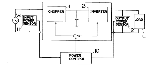
Referring now to FIG. 14, an inverter AC power supply is
shown in a general arrangement for easy understanding of the
present invention. The power supply comprises a chopper 1
and an inverter 2. The chopper 1 receives a low frequency
AC voltage from a commercial voltage source Vs and acts to
switch the voltage at a high frequency for providing a
smoothed DC voltage to a capacitor C. The inverter 2
received the smoothed DC voltage from the capacitor C to
switch the same to provide a high frequency AC voltage to a
load L. An input power sensor 11 is provided between the
chopper and the voltage source Vs to monitor an input power
Wl~ supplied to the chopper 1. Likewise, an output power
sensor 12 is provided between the inverter 2 and the load L
to monitor an output power Wo~ being supplied from the
inverter 2. A power controller 10 is connected to the
~0~281
.
- 26 -
sensors 11 and 12 in order to control, based upon the
monitored results, the switching of the inverter and the
chopper for equalizing the chopper input power Wl~ and the
inverter output power Wo~.
First embodiment <FIGS. 12 to 17>
FIG. 15 shows a circuit of the power supply in
accordance with a first preferred embodiment. The circuit
configuration is identical except for the power controller
10 to those of FIG. 1 which is explained in the summary of
the invention. The basic operation of the circuit is also
identical to the circuit of FIG. 1. Therefore, no further
explanation is deemed unnecessary for the basic circuit
arrangement and operation. However, it appears important
here to repeat the features of the circuit that:
1) An inductor L2 is inserted in series with the AC voltage
source VS across the rectifier input so as to counteract
c ~
the captivc reactance of capacitors Cl and C2 for
improving the power factor;
2) The chopper 1 and the inverter 2 shares switching
transistors Q1 and Q2 for effecting the chopper and the
inverter operations;
3) During the positive half cycle of the input AC source
voltage, Q1 is responsible for both of the chopper and
inverter operations, while Qz is responsible only for
the inverter operation, as shown in FIGS. 3A to 3D; and
4) During the negative half cycle of the input AC source
voltage, Q2 is responsible for both of the chopper and
~ - 27 - 2015281
inverter operations, while Q1 is responsible only for
the inverter operation, as shown in FIGS. 4A to 4D.
In addition, a low pass filter 3 is provided between the AC
voltage source Vs and the chopper 1 in order to obtain an
input current Ilu to the power supply circuit which is free
from being influenced by the high frequency switching
operation and therefore can retain a continuous wave form
with less distortion. In the circuit of FIG. ~, the
switching elements are bipolar transistors Ql and Ql
operating a frequency range around 40 KHz and the load is
shown to comprise a series combination of an inductor L3 and
discharge lamp FL [FCL-32EX/30 by Matsushita Denshi Kogyo,
Japan] with a preheating capacitor C4. Capacitor C4 iS
connected across filaments of the lamp FL to form a series
resonant circuit with inductor L3 for preheating the
filaments at the start of energizing the lamp FL. The
circuit is designed, for example, to have L2 = 0.95 mH, L3 =
1.02 mH, C2, C3 = 100 ~F so as to obtain an inverter input of
260V from the commercial AC voltage of lOOV and generate a
lamp current of 350 mA when driving Ql and Qz at a switching
frequency f = 40 KHz and at a duty ratio D = 35~. The duty
ratio D is determined in accordance with the above
definition II-B explained previously in the summary of the
invention.
For determination of the chopper input power Wlu, the
input power sensor 11 may be configured, for example,
l) to multiply the input voltage by the input current;
2) to analyze and process the waveform of a current flowing
20~281
- 28 -
into Lz; or
3) to process a current flowing into Q1 and Qz.
And, for determination of the inverter output power W0T, the
output power sensor 12 may be configured, for example,
l) to multiply a load current flowing to the load ~ a
load voltage developed across the load;
2) to calculate only from the load current;
3) to calculate only from the load voltage; or
4) to process a current flowing into Q1 and Qz.
In any case, it is required to determine Wl~ and WWT averaged
over at least one complete cycle of the input AC voltage.
Operation of the power controller l0 will be now
discussed with regard to the following operating conditions
where undesirable unbalancing of Wl~ and W~T takes place.
5 I. Light intensity control [Dimmer control]
Raising light intensity:
Starting from a balanced condition Wl~ = W~j at initially
selected frequency f (=f~) and duty ratio D = ~, as shown in
FIGS. 5A and 5B, when the switching frequency f is decreased
so as to correspondingly increase the light intensity or
W~T, there occurs an unbalanced condition WWT > Wl~ since W~T
shows a gradient greater than Wl~ with the frequency decrease
in an operational range from f0-, as shown in FIG. 6A, where
the switching frequency is shown as decreased from ~ to f1.
Upon occurrence of this unbalanced condition, the power
controller l0 responds immediately to control Q1 and Qz to
reestablish a balanced condition Wl~ = W~T while keeping W~T
fixed at the raised level, in accordance with the control
20~281
- - 29 -
mode [B] discussed previously with reference to FIGS. llA
and llB. That is, the control is made by firstly increasing
the duty ratio D [dl ~ d3] and then slightly decreasing the
switching frequency f [f1 ~ f3]-
Lowering light intensity:
When, on the other hand, the switching frequency f is
increased in order to correspondingly lower the light
intensity or W~T from the above starting condition of FIGS.
5A and 5B, there occurs another unbalanced condition WIN >
v~'c, ~ f
W~T since ~shows a gradient greater than Wl~ with the
frequency increase in an operational range from ~ as shown
in FIG. 7A, where the switching frequency is shown as
increased from f~ to f1. Upon occurrence of this unbalanced
condition, the power controller 10 responds immediately to
control Q1 and Q2 to reestablish a balanced condition Wl~ =
W~T while keeping WWT fixed at the lowered level, in
accordance with the control mode [D] discussed previously
with reference to FIGS. 13A and 13B. That is, the control
is made by firstly decreasing the duty ratio D [d1 ~ d3] and
then slightly decreasing the switching frequency f [f1 ' f3]
II. Differing lamp operating modes
Wl~ and W~T set balanced at a lamp-on mode:
For the power supply which is designed to have WIN = W~T
at a certain frequency f1 so as to provide a maintaining
voltage for keeping the lamp on, as shown in FIG. 16, it is
required at the start of igniting the lamp to drive Q1 and Q2
at a higher frequency f4 in order to allow capacitor C4 to
pass a preheating current through lamp filaments from the
~ 30 - 20~281
inverter output for preheating the filaments. After the
filaments are sufficiently heated, then the switching
frequency is lowered to f1 to develop a high voltage (gas
breakdown voltage) across capacitor c4, thereby turning on
the lamp. As apparent from FIG. 16, at the time of
preheating the filament with an increased switching
frequency f4, WWT sees a greater change than WIN thus causing
an unbalanced condition Wl~ > W~T. When such condition
continues to consume a greater Wl~ at the chopper than W~T at
the inverter output, an unduly high voltage will develop at
capacitor Cz and C3 and eventually break them. To avoid or
compensate for this unbalanced condition at the preheating
frequency f4, the power controller 10 responds immediately
to control Q1 and Qz to have Wl~ = W~T while keeping W~T fixed
at the lowered level, in accordance with the control mode
[D] discussed previously with reference to FIGS. 13A and
13B.
Wl~ and W~T set balanced at a preheating mode:
On the contrary, when the power supply which is designed
to have Wl~ = W~T at a preheating frequency f4, it will have
an unbalanced condition Wl~ < W~T in a normal lamp-on
operation at a switching frequency f, (c f4 ). To
reestablish the balanced condition Wl~ = W~T, the control is
made at the power controller 10 to increase WIN without
substantially changing W~T in accordance with the control
mode [B] discussed previously with reference to FIGS. llA
and llB.
- 20~5~2~1
- 31 -
III AC source voltage variations or fluctuations:
Raising in AC source voltage
When by some reason the AC source voltage is raised from
a rated voltage to cause an unbalanced condition WIN > WWT at
the selected frequency f1 and Dl, the power controller 10
operates, in accordance with the above control mode [B] of
FIGS. llA and llB, to compensate for such variation, thus
obtaining the balanced condition WIN = WWT without keeping
WWT substantially at a desired level.
Lowering in AC source voltaqe
When, on the other hand, the AC source voltage is
lowered from a rated voltage to cause an unbalanced
condition WIN < WWT at the selected frequency f1 and Dl, the
power controller 10 operates, in accordance with the above
control mode [D] of FIGS. 13A and 13B, to compensate for
such variation, thus obtaining the balanced condition WIN =
WWT without keeping WWT substantially at a desired level.
IV Load variations:
When the power supply is utilized to drive a number of
parallel coupled lamps FL1 to FL3, as shown in FIG. 17, Wl~
may vary depending upon the load conditions. For instance,
when any one of the lamps becomes extinct due to filament
breakage or lamp disconnection, the inverter output WWT will
be correspondingly decreased while the chopper input is
still maintained at a constant WIN determined at selected
frequency fl and duty ratio D1, leading to an unbalanced
condition WIN > WWT which would give unduly high voltage
stress to capacitor C2 and C3, switching transistors Ql and
~ - 32 - 20~281
Q2. That is, with the illustrated load configuration having
individual resonant circuits for the fluorescent lamps FL1
to FL3, even when one of the lamps FL1 to FL3 become extinct,
the output power of the other two lamps are kept
substantially unchanged so that the inverter output power
Wo~ is reduced to two-thirds (2/3) of the initial power.
~ For the multi-lamp driving operation, it is in most cases
required to keep the overall output power constant even when
one of the lamps becomes extinct. Therefore, it is
preferred to reestablish the balanced condition WIN = WWT
without causing substantial change in WWT. Such control can
be successfully made at the power controller 10 in
accordance with the above control mode [D] of FIGS. 13A and
13B.
Although, in the above embodiment, the control is made
by constantly monitoring WIN and WWT by obtaining input and
output currents or voltages, it is equally possible to
monitor harmonics superimposed in the input current as a
parameter representative of the relation between Wl~ and WWT
and to control to keep the monitored harmonic level below a
suitable threshold for maintaining the relation Wl~ and Wo~.
Second embodiment <FIGS. 18 to 27>
Referring to FIG. 18, a power supply in accordance with
/ ~ ~e/7 7~ 'o ,~2
a second embodiment of the present~is shown to additionally
include a source voltage polarity detector 20 which provides
an output indicating of the polarity of the AC source
voltage Vs to the power controller 10. The other circuit
arrangement is identical to the above first embodiment
- - - 33 _ 201~281
except that MOSFET (Metal Oxide Semiconductor Field Effect
Transistor) is utilized as first and second switching
transistors Q1 and Q2. In this circuit, parasitic diodes
intrinsic to MOSFETs are best utilized to form the first and
second diode D1 and D2 for reducing the number of components
of the circuit.
This embodiment is contemplated to regulate the chopper
input power ~l~ over a relatively wide range while causing
less influence on the inverter output power WOUT by ceasing
the chopper operation for a suitable time period while
substantially keeping the inverter operation. In other
words, one of the switching transistors Q1 and Q2 which is
responsible for the chopper operation is periodically ceased
or kept turned off while the other switching transistor is
being kept to turn on and off. As previously discussed with
reference to FIGS. 3 and 4, it is known that Q1 iS
responsible for the chopper operation and Q2 iS responsible
for the inverter operation during the positive half cycle of
the AC source voltage Vs, and vice versa during the negative
half cycle of the AC source voltage Vs. In this manner, the
switching element responsible for the chopper operation will
change between Q1 and Q2 in exact synchronism with the
polarity reversal of the AC source voltage and therefore can
be identified by the output of the polarity detector 20.
Therefore, the power controller 10 can control to
intermittently cease the chopper operation by selectively
disabling one of the switching transistors Q1 and Q2 thus
~ 34 ~ 2`~15~1
identified to be responsible for the chopper operation. As
shown in FIG. l9, Q1 and Q2 are controlled to intermittently
disabled for a suitable time interval in order to reduce WIN
to a desired extent while keeping the resulting variation in
the inverter output power WWT at a minimum. That is, when Q1
is disabled, for example, during the positive half cycle of
the AC source voltage Vs, the inverter output current I~ is
also ceased due to the fact that Q1 is also responsible for
the inverter operation. However, at this occurrence, Q2 is
still operating to effect the inverter operation such that
the instantaneous inverter output power is reduced to one
half only temporarily during the limited short interval
where Q1 is off, and therefore Wl~ can see only a less
reduction over the half cycle of the AC source voltage Vs.
In FIG. l9, ICH and IIN represent a chopped current and an
input current to the chopper, respectively. Accordingly, it
is found effective to use this control for compensation of
the unbalanced condition Wl~ > WWT with less attendant
variation in WWT. For example, this control is found
particularly suitable to compensate for the unbalanced
condition Wl~ > WWT which occurs at the time of lowering the
light intensity, as described with reference to the first
embodiment. That is, by intermittently ceasing the chopper
operation for a suitable off time interval TOFF within each
half cycle of the input AC source voltage Vs, as shown in
FIG. l9, the chopper input power WIN can be reduced to
reestablish the balanced condition WIN = WWT also at the
increased switching frequency without substantially causing
~ 35 ~ 201~281
the variation in W~T. It is noted at this time that, as
shown in FIG. 19, when the off time interval TOFF are set to
be evenly distributed over each half cycle of the input AC
source voltage Vs, it is possible to obtain an input current
IIN having a waveform analogous to that of the input voltage
Vs, thereby reducing harmonics as much as possible and
therefore maintaining an improved power factor. Although W
can be controlled over a wide range by suitably varying the
off time interval for ceasing the chopper operation, the off
time interval should be selected in association with the
design of the low pass filter 3 in order to avoid remarkable
harmonics superposed in the input current which would
otherwise lower the power factor.
Further, when the above control is combined with the
previously mentioned frequency control having inherent
characteristic of obtaining a greater change in WOUT with
less change in Wl~, it is possible to vary the WIN and WOUT
substantially independently, enabling a delicate control for
equalizing Wl~ and WOUT.
FIG. 20 shows a circuit which form a portion of the
power controller 10 to effect the above control of
intermittently ceasing the chopper operation. The circuit
includes an oscillator 30, a calibrator 31, and a switch
driver 32. The oscillator 30 is of general configuration
generating first and second oscillatory outputs OUT1 and
OUTz, as shown in FIG. 21, which are fed to the calibrator
i~rtogether with a polarity signal SGN issued from the above
source voltage polarity detector 20. The first oscillatory
~ - 36 - 201~281
output OUT1 and the polarity signal SGN are input through an
AND-gate G1 to a mono-stable multivibrator MV1 such that MV
is triggered to produce a signal P1 at a trailing edge of
the first oscillatory output OUT1 when SGN is high or the
input AC voltage V8 is positive. The signal P1, which is
set to have a predetermined width normally several times
greater than that of the switching cycle, is then fed to a
mono-stable multivibrator MV2 to trigger the same for
producing a signal P2 having the pulse width greater than
that of OUT1. The signal P2 is fed together with the
polarity signal SGN to an AND-gate G2 of which output is
inverted at a NOT gate G3 and is then fed to an AND-gate G4
together with the first oscillatory signal OUT1 so that AND-
gate G~ provides a driving signal DR1 for driving the
switching transistor Q1. In this manner, during the
positive half cycle of Vs, multivibrator NV2 generates at a
regular interval determined by multivibrator MV1 the signal
P2 which negates a portion of the first oscillatory output
OUT1 at that interval for obtaining a resulting first drive
signal DR1, thus enabling to periodically cease the chopper
operation. While, on the other hand, during the negative
~ o4~r`~e
half cycle of the input AC saucc voltage V8, the polarity
signal SGN is inverted at NOT gates G5 and G7, respectively
and is fed together with the second oscillatory output OUT2
to the like logic circuit so as to trigger a mono-stable
multivibrator MV4 at a regular interval determined by a
mono-stable multivibrator NV3 for generating a signal P4
which negates the second oscillatory output OUT2 and
~ 37 ~ 20~281
providing through an AND gate G10 a second drive signal DR2
for driving the switching transistor Q2, thus enabling to
periodically cease the chopper operation during the negative
half cycle.
FIG. 22 shows a circuit diagram which is common to the
multivibrators MV1 to MV4 utilized in the above logic. A
timer IC [NE555, by Signetics] is included to receive an
input at a trigger terminal [pin no.2] through a
differential circuit of resistors R11 and R12 and capacitor
~/f7
C11 such that the trigger terminal [pinc no. 2] sees a
voltage decrease as the input decrease. When the voltage at
the trigger terminal is decreased below l/3 of a control
voltage Vcc applied between an power terminal [pin no.8] and
p/~7
a ground terminal [pin no.l], an output terminal [pinc no.3]
is trigger to provide a High-level signal and at the same
time to make a discharge terminal [pin no.7] into a high
impedance state. Also, when a threshold terminal [pin no.6]
o~f~Oc~f
sees a voltage decrease down to below 2/3 of Vcc, the po~r
terminal [pin no.3] provides a Low-level signal and at the
same time the discharge terminal [pin no.7] goes "High". A
reset terminal [pin no.4] is connected to the power terminal
[pin no.8] and a frequency control terminal [pin no.5] is
connected to the ground terminal [pin no.l] through a
decoupling capacitor C13. The control voltage Vcc is applied
to a series circuit of a resistor R13 and a capacitor C12
which is coupled to the threshold terminal [pin no.6] and to
the discharge terminal [pin no.7] at the connection between
Ru and C12 and forms a time constant circuit for the timer
- 38 - 20~5281
IC, thus operating the timer IC as the mono-stable
multivibrator. That is, when the trigger terminal [pin
no.2] goes "Low-level", the output terminal [pin no.3] is
triggered to provide "High-level" signal for a time period
determined by Clz and R13 or until a voltage at the threshold
terminal [pin no.6] is dropped to a threshold voltage (= 2/3
Vcc), during which period the High-level signal at the
output terminal is maintained until a voltage at capacitor
Cl2 reaches the threshold voltage even when the input
terminal (pin no.2) see a voltage change. It is noted at
this time that a time constant of C12 and R13 is set to be
greater for the multivibrators MV1 and MV3 than for MV2 and
MV4 so as to obtain the output signals P1 to P4 of differing
pulse widths, as seen in FIG. 21.
Although the above control scheme of intermittently
ceasing the chopper operation is described with reference to
the chopper-and-inverter circuit of FIG. 18, it is of course
applicable to like circuits, as illustrated in FIGS. 23A to
23D, which have different connection points [A] and [B]
between the chopper and the AC voltage supply, and also to a
circuit of FIG. 24 in which another pair of switching
transistors Q3 and Q4 is added to form an inverter of full-
bridge configuration with Q1 and Q2, and in which a smoothing
capacitor Co is connected across Q3 and Q4 to provide an DC
voltage to the inverter. In the circuit of FIG. 24, Q3 and
Q4 are driven in synchronism respectively with Q2 and Q1 by
the same drive signals S2 and S1 to effect the same operation
as in the circuit of FIG. 18 except that the inverter
-- - 39 - ~ 81
produces an output voltage of a level approximately twice
that of the circuit of FIG. 18.
Further, the above control is also found effective to
drive an incandescent lamp LA with the like inverter and
chopper circuit, as shown in FIG. 25. In this operation
mode, the inverter provides to the incandescent lamp a lamp
current Iu having a rectangular waveform, as shown in FIG.
26 since there is no resonance circuit in the load. For
effecting a dimmer control of the lamp LA, it is found
effective to use the above control of intermittently ceasing
the chopper operation in place of controlling the switching
frequency since the frequency control has no effect on the
lamp current I~ for the incandescent lamp LA. That is, when
the lamp LA is required to be dimmed, for example, from a
max light intensity condition as shown in the upper part of
FIG. 26, one of the switching transistors Q1 and Qz
responsible for the chopper operation is controlled to be
intermittently disabled, as shown in the lower part of FIG.
26, so as to reduce an input current to the chopper or the
chopper input power Wl~, thereby correspondingly reducing a
DC voltage developed at capacitors Cz and C3. Therefore, the
input power to the inverter is also decreased to
correspondingly reduce the inverter output power Wo~ or the
light intensity as desired. Thus, the dimmer control for
the incandescent lamp LA can be successfully in the power
supply of the present invention by controlling to
intermittently cease the chopper operation. It is noted at
this time that Wl~ and Wo~ can be substantially balanced in
~ 40 - 2015281
this dimmer control with or without the control of the duty
ratio.
Furthermore, to drive the incandescent lamp LA with the
circuit of FIG. 25, it is also possible to control Q1 and Q2
in a manner, as shown in the upper part of FIG. 27, to
operate only Q1 during the positive half cycle of the input
AC source voltage Vl~ and only Qz during the negative half
cycle of Vl~. In this mode, the power circuit provides a
lamp current Iu in the form of repeating pulses of which
polarity is reversed in synchronism with the polarity
reversal of Vl~ such that lamp current I~ has an effective
value which is one half of the peak value. So long as the
input AC source voltage Vl~ is maintained at a fixed level,
the power supply operates in the manner, as shown in the
upper part of FIG. 27 to drive the lamp LA appropriately
while maintaining a balanced condition Wl~ = W~T. When by
some reason the AC source voltage is increased, a control
can be made, as shown in the lower part of FIG. 27, to
intermittently disable Q1 and Q2 respectively in the positive
and negative half cycles of Vl~ so as to compensate for the
input AC voltage increase and keep the input power Wl~ at a
fixed level irrespective of the input AC voltage increase.
During this control of reducing the input power, it is also
controlled, as shown in the lower part of FIG. 27, to turn
on Q2 immediately after Q1 is turned off within the positive
half cycle of Vl~ and to likewise turn on Q~ immediately
after Qz is turned off within the negative half cycle of Vl~,
whereby maintaining the effective value of the lamp current
- 41 - ~ ~`5~1
I~ to be one half of the peak value and therefore
maintaining the inverter output power W0T constant at a
desired level. With this consequence, the output power or
the light intensity of the lamp can be kept free from the
variation possible in the input AC source voltage.
Third embodiment <FIGS. 28 to 46>
An third embodiment of the present invention is
contemplated to additionally include means to cease only the
chopper operation when the load is disconnected in order to
avoid undue voltage increase or power consumption at the
chopper which would lead to the breakage of the circuit
components, particularly the switching transistors and the
capacitors which store input energy and provide the inverter
input. As shown in FIG. 28[22], an inverter AC power supply
in accordance with the present embodiment includes, in
addition to the like chopper and inverter circuit as
discussed in the previous embodiments, an off-load detector
40 for detecting an off-load condition, a like source
voltage polarity detector 20 as utilized in the second
embodiment, and a controller 50. Although the controller 50
effects the above power control of balancing WIN and W~T in
cooperation with an input power monitor and an output power
monitor as discussed in the first embodiment, duplicate
explanation of such power control is avoided in the
following description and drawings. The controller 50 is
configured in the present embodiment to control the
switching transistors Q1 and Qz in accordance with detected
results from detectors 20 and 40 so as to disable the
2015281
- 42 -
chopper operation so long as the load L is disconnected, yet
keeping the inverter operation to make the inverter ready
for providing a load current as soon as the load is
disconnected. With this consequence, it is readily possible
to detect the re-connection of the load by monitoring such
load current to thereby facilitate the design of restarting
the load. As previously discussed, Q1 and Q2 in the
chopper/inverter circuit of FIG. 28 can be identified by the
polarity sensor 20 as to whether or not they are currently
responsible for the chopper operation. Accordingly, the
controller 50 can, in response to the outputs from the
individual detectors 20 and 40, control to disable Ql in the
positive half cycle and Q2 in the negative half cycle of the
input AC source voltage Vl~ for disabling the chopper
operation while allowing the inverter operation. In detail,
the polarity detector 20 is configured to provide a polarity
signal SGN which goes "High" when Vl~ > 0 and goes "Low" when
Vl~ < 0. The off-load detector 40 is also configured to
provide a load signal NL which goes "High" when no load
condition is detected and otherwise remains "Low". The
controller 50 include a logic, as shown in FIG. 29, in which
Bl and 8z are drive signals generated from an oscillator (not
shown) provided in the controller 50 to drive Q1 and Q2,
respectively. In operation, when the load signal NL is low
as indicative of that the load is connected, OR-gates G3 and
G4 are both operative to provide "High-level" output such
that AND-gates Gs and G6 are both enabled to pass the drive
signals Sl and Sz, irrespective of the polarity signal SGN,
201 528~
,
- 43 -
whereby maintaining the normal operation of effecting the
chopper and inverter operations. When the load signal NL
goes "High-level" as indicative of that the load is
disconnected, OR-gates G3 and G4 will be made in the same
conditionas AND-gates G1 and G2 to effect the followings:
1) When the polarity signal 8GN is "High" as indicative of
Vl~ > O, AND-gate G2 goes "High" to thereby provide S2
from AND-gate G6 for enabling to turn on and off Q2 or
keeping the inverter operation. At this condition,
however, AND-gate G1 goes "Low" to render AND-gate Gs
"Low", ceasing to provide S1 and therefore disabling the
chopper operation; and
2) When 8GN goes "Low" as indicative of Vl~ < O, AND-gate G
turns to have "High-level" output to thereby allow AND-
gate G5 to output S1 for enabling the inverter operation.
At this condition, AND-gate G2 goes "Low" to thereby
keep the output of AND-gate G6 "Low", thus inhibiting to
provide 81 to Q1 and therefore disabling the chopper
operation.
The above control scheme is seen in FIG. 30 in terms of
waveforms at the individual outputs, from which it can be
confirmed that so long as the load signal NL remains "Low",
S1 and S2 are generated to effect the chopper and inverter
operations irrespective of the polarity signal SGN level,
and that after NL goes high (at time to) the output of S1 is
inhibited when 8GN is "High" and the output of S2 is
inhibited when æGN is "Low". In the figure, S1 and S2 are
depicted to have a relatively long cycle for illustration
20 1 523 1
- 44 -
purpose only, but are in fact to have a much shorter cycle
than illustrated.
The polarity detector 20 is coupled to the
chopper/inverter circuit to detect the instantaneous
polarity of the input AC voltage by monitoring currents or
voltages at suitable points which may include, for example,
points designated in FIG. 31 at:
(a) for input AC current;
(b) for input AC voltage;
(c) for chopper current;
(d) for voltage at inductor L2 for chopper operation by
means of an additional secondary winding, for instance;
(e),(e') for current through D4 or D3;
(f),(f') for voltage across D4 or D3;
(g),(g') for current through Q2 or Q1;
(h),(h') for voltage across Q2 or Q1; and
(i),(i') for load current within the inverter circuit.
The points (a),(c),(e),(e'),(g),(g'),(i),(i') are for
monitoring the currents which are not present in the off-
load condition, and are therefore found only effective to
detect an on-load condition and not the off-load condition.
Also point (d) is found only effective only in the on-load
condition and not in the off-load condition, since the
intended voltage will not develop across L2 in the absence
of a current therethrough. While, on the other hand,
(h),(h') is found effective in the off-load condition but
not in the on-load condition since the voltage across Q1 or
Q2 will change depending upon the polarity of the input AC
20 1 528 1
voltage at the off-load condition but will be of rectangular
wave synchronized with the drive signal S1 or s2 having no
relation to the polarity of the input AC voltage. With this
7~7ere fo~e
consequence, ThcrcfGl~, points (b), (e), or (e') is found
suitable to monitor the polarity both in the off-load and
on-load conditions, although it may of course possible to
use different points for monitoring the polarity separately
in the on-load condition and in the off-load condition.
The off-load detector 40 is coupled to the
chopper/inverter circuit or the load by monitoring currents
or voltages at suitable points which may include, for
example, points illustrated in FIG. 32A and 32B at:
(j),(j') for current through Q2 or Q1;
(k),(k') for voltage across Q2 or Q-;
(e) for load current on the load side;
(m),(m') for load current within the inverter;
(n) for current through C3;
(o) for voltage across c2 and C3;
(p) for voltage across L3 in the load circuit through
additional secondary winding; and
(q) for voltage at one end of lamp FL.
The above points are effective to detect not only the off-
load condition but also the on-load condition. This is
because that even after the chopper operation is suspended
in response to the off-load detection, the inverter
operation is controlled to be still operating such that, as
soon as the load is reconnected, the inverter can
immediately provide through the active one of Q- and Q2, the
- 46 - 20a~81
load and C2 and C3 a load current with a corresponding
voltage change by which the on-load condition can be
detected. Although the above points are effective for
monitoring both the off-load and on-load condition, the off-
load condition alone may be detected by the use of a thermo-
sensor monitoring a temperature of the load or switching
elements or by the use of an optical sensor monitoring a
light energy from the lamp FL in case it is connected as the
load.
FIG. 33 illustrates one example for detecting the source
voltage polarity and the off-load condition in the above
chopper/inverter circuit. The polarity is detected by
monitoring a voltage across diode D4 at [J] by the use of a
voltage divider of R1 and Rz, and the off-load condition is
detected by monitoring a load current at [X-Y] by the use of
a current transformer CT inserted in series with the load
between the inverter output ends A and B. When the load is
disconnected to open the inverter outputs ends A and B, a
voltage [X-Y] at a secondary winding of CT is decreased to
zero for indicate the off-load condition. At this off-load
condition, Ql and Q2 are controlled to be selectively
disabled depending upon the input AC source voltage polarity
detected at [J] (Q1 while Vl~ > 0, Q2 while VIN < O) for
ceasing the chopper operation while keeping the inverter
operation, as discussed hereinbefore. When the load is
reconnected, the load current is caused to flow between the
inverter output ends A and B from either of C2 or C3,
providing a corresponding voltage at [X-Y] to thereby
2~
enabling the detection of the on-load condition and restart
of the circuit in a suitable manner.
FIG. 34 illustrates one example of the source voltage
polarity detector 20 for use with the circuit of FIG. 33.
The detector 20 has inputs connected to points [J] and [G]
in the circuit of FIG. 33 and includes a capacitor C7. When
the source voltage Vl~ > 0, diode D4 sees a high reverse bias
which is divided by resistors R1 and Rz to provide at [J] a
corresponding voltage by which capacitor C7 is charged to a
certain level above a reference voltage determined by
resistors Rs and R6 such that a comparator CP1 outputs the
"High-level" polarity signal SGN. When, on the other hand,
Vl~ < 0, diode D4 sees a small forward bias so that capacitor
Q7 is discharged to have a corresponding voltage level at
the input of comparator CP1 lower than the reference
voltage, whereby the "Low-level" polarity signal SGN is
output from comparator CP1.
FIG. 35 illustrates one example of the off-load detector
40 adapted in use to the above circuit of FIG. 33. During
the on-load condition, the current transformer CT generates
between points [X-Y] an alternating voltage which is applied
through a diode bridge rectifier DB to charge a capacitor C6
to a level higher than a reference voltage determined by
resistors R3 and R4 such that a comparator CP2 provides the
"Low-level" load signal NL. Upon the off-load condition, no
voltage is developed between [X-Y] and therefore that no
current is supplied to capacitor C6 so that capacitor C6 will
be discharged down below the reference voltage, whereby
- 48 - ~0 ~ 81
comparator CP2 turns to output the "High-level" load signal
NL. To expedite the discharging of C6 at the off-load
condition, C6 may be connected in parallel with additional
discharging capacitor or may have less capacitance.
FIG. 36 illustrates another preferred set of points for
detection of the source voltage polarity and the off-load
condition in the like chopper/inverter circuit when the
circuit is used for driving the load including a series
resonance circuit of an inductor L3 and a capacitor C5
connected in parallel with the lamp FL. In this
modification, the voltage polarity is detected by monitoring
input AC voltage Vl~ between points [M-N], while the off-load
condition is detected by monitoring a current through Ql by
the use of a current transformer CT as well as by monitoring
a current through Q2 by a resistor Ro. When the lamp FL is
disconnected as indicated in the figure, although a current
will flow through the series resonance circuit of L3 and C4
between the inverter output ends A and B, such resonance
current is substantially a reactive current hardly consuming
the output power, thus causing also the off-load condition.
However, as seen from FIG. 37 illustrating waveforms for
input AC voltage Vl~, current iL through inductor L3, voltage
Vcs at capacitor C5, the circuit of FIG. 36 will see a
current for a short time interval each time the voltage
polarity is reversed, which invalidates to detect re-
connection of the load simply by monitoring the current
through the switching transistors. To avoid this
inconvenience and assure reliable reconnected load
9- 2~ 81
detection, it is preferred either to stop the detection for
a time interval in which such current continues or to
average such current over an extended period for valid
comparison with a reference value.
FIG. 38 shows one example of the source voltage polarity
detector 20 in which the input AC voltage Vl~ received at
terminals tM-N] is step down at a transformer Tf and is
rectified by diode Ds to provide at resistor R7 a
corresponding voltage VR which is to be compared at a
comparator CP1 with a reference voltage determined by
resistors Rs and R6. When Vl~ > O, a high voltage VR is
developed at R7 which is greater than the reference voltage
so that CP1 outputs the "High-level" polarity signal SGN.
When Vl~ < O, no voltage is developed at R7 so that CP1
outputs the "Low-level" polarity signal 8GN. It is noted at
this time that, although the reference voltage is required
to be as low as possible in the sense of balancing the
"High-level" period and the "Low-level" period of the
polarity signal ~GN, it is preferably set to be a certain
high level enough for discriminating a possible noise in the
detector and therefore assuring a reliable detection, since
a noise voltage at R7 might cause CP1 to erroneously output
the "High-level" signal SGN.
FIG. 39 illustrates one example of the off-load detector
40 utilized in the circuit of FIG. 36. While the load is
connected to flow a current through transistor Q1 (or diode
D1), the current transformer CT generates between a point
[X] and a ground [G] an alternating voltage which is applied
- 50 - 2~
as being rectified by a diode D7 to charge a capacitor Cs to
a level higher than a reference voltage determined by
resistors Rs and R10 such that a comparator CP3 provides a
"High-level" output. Also in the on-load condition,
transistor Qz [or diode d2] sees a current which provides a
corresponding AC voltage between a point [K] and the ground
[G] which voltage is then rectified through diode D6 to
charge a capacitor C6 to a level higher than a reference
voltage determined by resistors R3 and R4 such that a
comparator CP2 provides a "High-level" output.
When, on the other hand, the load is disconnected to
discontinue a current through Q1 (or d1), capacitor Cs will
discharge through resistor R11 down to a voltage below the
reference voltage at CP3, thereby producing a "Low-level"
output from CP3. Also in the off-load condition, no current
flows through Q2 (or d2), capacitor C6 will discharge through
resistor Rs down to a voltage below the reference voltage at
CP2, thereby producing a "Low-level" output from CPz. The
outputs from CP2 and CP3 are gated at NAND-gate G11 to finally
provide the load signal NL which goes "High" when any one of
the outputs from CP2 and CP3 is "Low", and which goes "Low"
only when both outputs are "High", thus assuring reliable
off-load and on-load or reconnected load detection.
Further, for detecting the re-connection of the load in
the circuit of FIG. 36, it may be also effective to operate
only one of switching transistor Q1 and Q2 after detection of
the off-load. For example, when only Qz is kept to turn on
and off at Vl~ > 0 with Q1 is disabled or kept turned off
20 1 528 1
- 51 -
irrespective of the input voltage polarity, capacitor
voltage VC5 at C5 is kept constantly equal to capacitor
voltage (- VC3) at C3 and a current will flow only for a
short time period 8T after the first reversal of voltage
polarity following the detection of the off-load condition,
,,v, //
as seen in FIG. 40, and no current fill flow until the load
is reconnected. With this scheme, therefore, the re-
connected condition can be detected by monitoring a current
in the circuit only at one point and simply by ignoring the
current appearing within such initial short time period ST
subsequent to the first polarity reversal of the input
voltage, which makes it possible to simplify a control
circuit arrangement. Although the above scheme is not
capable of detecting the re-connected load condition while
Vl~ < 0, such condition can be detected successfully in the
subsequent half cycle of Vl~ > 0 and such delay is of no
consequence in the actual use. It is of course equally
possible to keep only operative Q1 in contrast to the above
explanation. It should be noted at this time that the above
control scheme is also applicable to the circuit of FIG. 28.
Referring to FIG. 41, a further arrangement is shown for
detection of the input voltage polarity and the off-load
condition in the like chopper/inverter circuit, The input
voltage polarity is detected at points [M-N] in the same
manner as described hereinbefore with reference to FIG. 38.
In this modification, a voltage divider of resistors Rl2 and
R13 is coupled across the series circuit of capacitors C2 and
C3 so as to provide a monitor output voltage between points
20 1 ~28 1
- 52 -
[P-G] for detection of the off-load condition and the re-
connected load condition by that voltage. Upon occurrence
of off-load condition, the chopper output will be all stored
in capacitors Cz and C3 without being consumed by the load to
thereby correspondingly increase capacitor voltage and the
monitor voltage [P-G]. Therefore, the off-load condition
can be easily detected by the increase in the monitor
voltage. At this occurrence, the chopper operation is
inhibited by controlling to disable one of Q1 and Qz
currently responsible for the chopper operation as
identified by the polarity signal SGN, as explained
hereinbefore. When the load is reconnected, one of
capacitors Cz and C3 will provide a current through active
one of Q1 and Q1 to the load and therefore sees a voltage
drop which results in a corresponding voltage drop at [P] by
which the re-connected load condition can be easily
detected.
As shown in FIG. 42, during the off-load condition
[starting from to] in which the chopper operation is
controlled to be disabled by turning off the corresponding
one of the switching transistors responsible for the chopper
operation [i.e., Q1 in positive half cycle and Qz in the
negative half cycle of Vl~], it may be effective to keep on
the other switching transistor responsible only for the
inverter operation [i.e., Qz in the positive half cycle and
Q1 in the negative half cycle of Vl~] rather than to turn on
and off. With this control, power requirement for driving
the switching transistors can be reduced, particularly in
20 1 5~8 ~
- 53 -
the circuit utilizing power MOSFET as Q1 and Q2 which
requires charging and discharging at gate each time it is
turned on and off. Also in this control, drive signals S1
and SA'(for Q1 and Q2) are apparently to be inverted signal
of the polarity signal 8GN during the off-load condition, as
seen in the figure. Such drive signals S1 and S2 can be
generated by a logic circuit of FIG. 43. It should be noted
in this connection that this control can be well adapted to
the circuits of FIGS. 28, 33, and 36.
FIG. 44 illustrates a further arrangement for detection
of the input AC voltage polarity and the off-load condition
with regard to a modified chopper/inverter circuit. The
modified circuit is similar in configuration to that of FIG.
28 except for particular capacitor location in the inverter.
For an easy understanding purpose like numerals are repeated
to designate like components serving like circuit
operations. In this modified circuit, capacitors C2 and C3
are connected in circuit to provide a DC voltage to the
input of the inverter. Capacitor C2 is a smoothing
capacitor connected across the across a series pair of first
and second transistors Ql and Q2, while capacitor C3 is
Se ~
connected in series with the load L across the fir3t
transistor Q2.
In operation, when transistor Ql is on while transistor
Q2 is off during a positive half cycle of the input AC
voltage, the voltage source VS flows a current of increasing
magnitude through inductor L2, third diode D3, transistor Ql
2015281
- 54 -
and back to the voltage source VS to store energy into the
inductor L2. At the same time, transistor Ql also acts to
flow a current from capacitor C2, through Ql, capacitor C3,
load L, and back to capacitor C2 to provide a load current
in one direction. Subsequently, when transistor Ql is off
and in stead transistor Q2 is on within the same positive
half cycle, inductor L2 releases its energy through third
diode D3, capacitor C2, diode D2, and voltage source VS to
accumulate a smoothed DC voltage into capacitor C4. At this
occurrence, transistor Q2 operates to flow a current from
capacitor C3, Q2, load L, and back to C3, thus providing a
load current in the opposite direction.
During the negative half cycle of the input AC voltage,
when transistor Ql is off while transistor Q2 is on, the
voltage source V8 flows a current through Q2, fourth diode
D4, inductor L2 back to Vs to store energy into inductor L2.
At this occurrence, transistor Q2 operates to flow a load
current in one direction from capacitor C3, Q2, and load L.
Subsequently when transistor Ql is on and in stead Q2 is off,
inductor L2 release its energy through V8, first diode Dl,
capacitor C2, fourth diode D4 and back to inductor L2 for
charging capacitor C2, while inductor L2 also supplies a
current through V8, capacitor C3, load L, diode D4. At the
same time, transistor Ql operates to flow a load current in
the opposite direction from capacitor C2, through Ql,
capacitor C3, and load L. In this manner, switching
transistors Ql and Q2 repeat alternately conductive and non-
20 1 523 1
- 55 -
conductive for effecting the inverter operation of applying
a high frequency AC voltage to load L while at the same time
effecting the chopper operation of charging capacitors C2
and C3 through inductor L2 and diode-bridge rectifier of Dl
to D4 in such a way as to provide the smoothed voltage to
the inverter input. Accordingly, it is confirmed in this
modified circuit that Q1 is responsible for the chopper and
inverter operations and Q2 is responsible only for the
inverter operation during the positive half cycle and vice
versa in the negative half cycle of the input AC voltage.
Further, in the modified chopper/inverter circuit, coupling
capacitor C3 is selected to have capacitance larger enough
than capacitor C4, which is connected in parallel with lamp
FL to effect preheating the filament thereof as well as to
form a resonance circuit with inductor L3 in the load, so
that it will not influence the resonance circuit. As is
known from the above discussion, coupling capacitor C3 acts
to provide a DC voltage to the inverter input when Q2 is on
and also acts to filter a dc component in the load current,
and therefore can have less capacitance relative to
smoothing capacitor C2. For example, the circuit may be
designed to have C2 = 100 ~F, C3 = O.47 ,uF, C4 = O. 0015 ,uF
when L2 = O. 5 mH, L3 = O. 45 mH are selected for driving a
fluorescent lamp [FCL-32EX/30, by Matsushita Denshi Kogyo,
Japan] at a switching frequency of 40 KHz from the input
voltage of 100 V.
The above modified circuit may be controlled in the same
-
- 56 - 201~81
manner as discussed with reference to FIG. 30 or FIG. 37 for
ceasing the chopper operation upon detection of the off-load
condition while keeping the inverter active for detection of
re-connected load condition. In this respect, it may be
preferred to keep operating only Q1 after the off-load
condition for reliable detecting the re-connection of the
load, in view of that, even when Q2 is kept operating in the
off-load condition in an attempt to provide a load current
from C3 for detection of re-connection of load, C3 of less
capacitance may be exhausted by natural discharging in the
off-load condition and may fail to provide the load current.
The input voltage polarity of the above circuit can be
detected by monitoring a voltage between points [J-G] with a
like detector circuit as shown in FIG. 34. The off-load
condition can be also detected by monitoring a voltage
across a resistor Ro inserted in series with Q2 with the use
of a detector circuit as shown in FIG. 45.
It is noted at this time the above modified
chopper/inverter circuit can be equally utilized in the
previous embodiments without causing any substantial problem
in the control of equalizing the chopper input power Wl~ and
the inverter output power Wo~.
FIG. 46 illustrates another modified chopper/inverter
circuit in which an additional resonance capacitor C5 is
connected across the lamp FL. For reliably detecting the
re-connection of the load with this circuit, it is also
effective to keep operating only Q1 during the negative half
cycle of the input AC voltage. Otherwise, Q2 would operate
~ 57 ~ 201~
to discharge C3 and C5 substantially entirely, failing to
provide a load current at the subsequent re-connection of
the load, thus failing to detect the re-connected load
condition. Furthermore, if C3 and C5 have been exhausted,
they would be charged at the conduction of Q1 to thereby
generate an erroneous load current leading lc~d~ to false
detection of the re-connected condition such that the
control has to be required to ignore such false current by
additional scheme as discussed previously with reference to
FIGS. 36 and 37. However, by keeping only Ql operative in
the negative half cycle of the input AC voltage over the
off-load condition, C3 and C5 can be charged in a manner as
to have a relation VC3 + Vc5 = Vc2 SO that a load current will
not flow until the load is reconnected, thus making it
possible to detect the reconnected load condition by
monitoring a load current flowing through the switching
transistor.
It is noted at this time that the various controls
described in the above for detection of the re-connected
load condition can be equally applicable to all the circuits
of the present invention including those of FIGS. 23 and 24.
Fourth embodiment <FIGS. 47 to 56>
The power control of the present invention is also
applicable to cases where the above chopper/inverter circuit
is required to provide a relatively low frequency voltage or
current of generally rectangular waveform of less high
-t'r o/~t
frequency component resulting form the high frequency
switching of Q1 and Qz. For instance, when the circuit is
- 2Q~
- 58 -
utilized to drive a discharge lamp DL by a relatively low
frequency load current of generally rectangular waveform of
less high frequency component, as shown in FIG. 49 in order
to avoid acoustic resonance which would occur when the lamp
is driven by a high frequency current. FIG. 47 illustrates
a circuit arrangement for producing the low frequency load
current which is identical in configuration to the previous
embodiment but in which Q1 and Qz are controlled somewhat
differently. That is, as shown FIG. 48, Ql turns on and off
at a high frequency while Q2 is kept turned off during the
positive half cycle of the input AC voltage VIN and vice
versa during the negative half cycle of Vl~ so as to provide
an inverter output V a train of high frequency pulses of
which polarity is reversed at a low frequency or in
synchronism with the low frequency input AC voltage Vl~. The
circuit includes a bypass capacitor C5 which is connected
across the lamp DL to pass therethrough substantially all of
high frequency component of the inverter output V, thereby
applying to the lamp DL a load current I~, as shown in FIG.
49, which sees only a slight amount of the high frequency
component and presents a generally rectangular waveform
having the same low frequency of the input AC voltage Vl~.
With this result, the lamp DL can be driven without causing
the acoustic resonance leading to unstable arc and
eventually to flickering or extinction of the lamp.
FIG. 50 illustrates another scheme of driving Q1 and Q2
of the circuit of FIG. 47 in order to obtain a load current
of FIG. 51. The load current is characterized to comprise a
- 59 -
low frequency part of generally rectangular waveform of FIG.
49 alternated by high frequency part which appear for a
limited time interval T3 around each polarity reversal of
the input AC voltage Vl~. Such composite current Iu is found
advantageous to operate the lamp DL stably while preventing
the unacceptable acoustic resonance. For generating the
composite current Iu, the circuit is controlled to operate
only one of Q1 and QZ selectively depending upon the polarity
of the input AC voltage VIN [Q1 for time period T1 of VIN >O,
Q2 for time period T2 of VIN <O] as discussed in the above
with reference to FIG. 48, and at the same time to turn on
and off alternately for the limited time interval T3 around
the polarity reversal of VIN.
FIG. 52 illustrates another chopper/inverter circuit for
providing a train of high frequency output pulses of which
polarity is reverse at a low frequency in synchronism with
the input AC voltage. The circuit comprises four switching
transistors Q1 to Q4 connected in full-bridge configuration
and a smoothing capacitor Co connected in parallel across
the series pair of transistors Q3 and Q4. A load L is
illustrated as an inductive load having an inductor and
resistor. As shown in FIG. 53, during a first time period
T1 or the positive half cycle of Vl~, Q1 is driven to turn on
and off at a high frequency and Q4 is kept turned on, while
the other diagonally opposed Q2 and Q3 are kept turned off.
In the subsequent time period T2 corresponding to the
negative half cycle of VIN, Q2 is driven to turn on and off
at the same high frequency with Q3 kept turned on, while Q1
`- 2015281
- 60 -
and Q4 are kept turned off. Whereby, the inverter can
provide to the load a resulting output in the form of a high
frequency pulse train of which polarity is reversed at the
low frequency in synchronism with the input AC voltage. In
this circuit having the full-bridge transistor
configuration, the load L can receive a full voltage of the
Co which almost doubles that obtained in the circuit of FIG.
47. Thus, the above circuit is particularly effective where
it is required a high load voltage. In the above control of
FIG. 53, Q3 and Q4 are driven in synchronism with VIN,
however, they can be driven to turn on and off at the same
high frequency in synchronism with Q2 and Q1, respectively.
In such case, upon turning off of Q1 and Q4 an energy stored
in the inductor of the load L will flow through a closed
loop of diode D5, capacitor Co, diode D2, and load L, and
upon turning off of Q2 and Q3 the energy will from the
inductor through another closed loop of diode D1, capacitor
Co, diode D6, and the load L. Further, it is equally
possible to operate Q1 and Q2 to turn on and off alternately
over the full period of T1 and T2, while operating Q3 and Q4
in synchronism with Vl~.
FIG. 54 illustrates an arrangement for balancing the
chopper input power Wl~l and the inverter output power W~UT
with regard to the like chopper/inverter circuit of FIG. 47
operating in the like manner of FIGS. 48 or 50 to provide an
output of FIGS. 49 or 51. To this end, a power controller
10 is included in combination with an input power sensor 11
and an output power sensor 12. The input power sensor 11 is
- 2~-~S;2~1
- 61 -
connected in circuit to monitor a DC voltage across
capacitors C2 and C3 which is the function of the chopper
output voltage and therefore indicative of the chopper input
power Wl~. The output power sensor 12 is connected in
circuit to monitor a load current as indicative of the
inverter output power WWT. Due to the inclusion of a bypass
capacitor C5 connected across the discharge lamp DL for
bypassing high frequency component as mentioned previously
in the circuit of FIG. 47, the load including inductor L3
and capacitor C5 will have a natural frequency fC rather
smaller than and spaced from a switching frequency f at
which Ql and Q2 are driven to provide a train of rectangular
pulses within each half cycle of Vl~. For instance, f C = 10
- 20 KHz at f = 40 KHz. Accordingly, WWT will show a rather
gradual change with a change in the switching frequency f
within an operational range relative to the case where f C is
close to f [for example, f C = 30 KHZ at f = 40 KHZ], as seen
in FIG. 5A, for providing a high frequency alternating
output. This means that only less difference between WIN and
WWT is caused when varying the switching frequency f in
order to regulate WWT or Wl~ for dimmer control or
compensation for an input AC voltage variation. Therefore,
when required to balancing Wl~ and WWT in accordance with the
control schemes of FIGS. 10 to 14, the amount of variation
in the switching frequency f as well as duty ratio D can be
retained rather small, thereby facilitating the control of
balancing the Wl~ and W~T. For example, when it is required
to dim the lamp DL from a maximum light intensity condition
` - 62 - 20~
of FIG. 55A to a reduced light intensity condition of FIG.
55B, the balancing of Wl~ and W~T can be re-established also
at the dimmed condition by controlling both of the switching
frequency f and duty ratio D in accordance with the control
scheme as described with reference to FIGS. 13A and 13B but
with less variations in f and D. It is noted at this time
that, as shown in FIGS. 55A and 55B, the resulting output
current Iu from the circuit of FIG. 54 can be shaped to have
generally rectangular waveform from which high frequency
components have been removed by the bypass capacitor C5 and
have a low frequency in synchronism with the input AC
voltage Vl~.
Also with regard to the above circuit of FIG. 54
operating to provide the low frequency output of generally
rectangular waveform, it is equally possible to combine the
previously mentioned control of intermittently ceasing the
chopper operation to regulate the chopper input power Wl~
relatively independently of the inverter output power W~T,
as discussed in the second embodiment. In this case, as
shown in FIG. 56A, one of Q1 and Q1 currently responsible for
chopper operation is disabled periodically at a regular
interval to reduce Wl~. Further, it is also possible to
combine the control of detecting the off-load and
reconnected load conditions as discussed in the third
embodiment of the present invention, in which case, one of
Q1 and Q2 responsible for the chopper operation is likewise
disabled upon detection of the off-load condition, as shown
in FIG. 56B, while the other one of Q1 and Q2 is kept
`~ - 63 - 20~81
operative so that the circuit is ready for provide a load
current as soon as the load is reconnected.
In the above embodiments and modifications, although the
load is mainly shown to comprise a lamp with inductor and
capacitor for easy understanding purposes, the present
invention should not be understood to be limited thereto and
is equally effective to drive various loads including a
resistive load and other inductive loads as exemplarily
shown in FIGS. 57A to 57D.