Note: Descriptions are shown in the official language in which they were submitted.
CA 02015301 1998-11-27
1
TRANSPARENT OPTICALLY VARIABLE LEVICE
This invention relates to a transparent optically
variable device.
Optically variable devices are disclosed in U.S.
Patents Nos. 4,705,300 and 4,705,356. Optically variable
devices which can be used in optically variable inks and
optically variable pigments are known. However, those
optically variable devices are opaque. There is a need for
optically variable devices where some transparency can be
obtained.
In general, it is an object of the present invention
to provide an optically variable device which has some degree
of transparency.
Another object of the invention is to provide an
optically variable device of the above character which can be
utilized in various different types of applications.
Another object of the invention is to provide an
optical variable device of the above character which has good
color purity.
Another object of the invention is to provide an
optically variable device with as few as three layers making
possible a lower cost device which can be manufactured on roll
coating equipment.
Another object of the invention is to provide an
optical variable device of the above character which can be
utilized in inks, as optically variable pigment.
According to the invention there is provided a
transparent, optically variable device having a symmetric
61051-2386
CA 02015301 1998-11-27
2
three-layer interference coating, said three-layer coating
comprising first and second partially transmitting absorber
layers, said absorber layers having substantially the same
composition and thickness and a dielectric spacer layer
disposed between the first and second absorber layers, said
absorber layers being from 20 to 50~ transmitting.
Additional objects and features of the invention
will appear from the following description in which the
preferred embodiments are set forth in detail in conjunction
with the accompanying drawing.
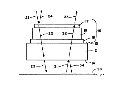
Figure 1 is a cross-sectional view of a transparent
optically variable device incorporating the present invention.
Figure 2 is a view showing the manner in which light
is reflected from the optically variable device of the present
invention which with angle shift provides a shift from one
color to another.
Figure 3 is a graph of reflectance of a transparent
green-to-blue optically variable device incorporating the
present invention.
More particularly as shown in the drawings, the
optically variable device 11 is comprised of a substrate 12
having a first surface 13 and a second
61051-2386
201530.
-3-
surface 14. In accordance with the present invention
the substrate 12 should be formed of a transparent
material. One material found to be satisfactory is a
polymeric substrate formed, for example of
polyethylene terephthalate. A symmetric three-layer
coating 16 is carried by the first surface 13 of the
substrate 12. The three-layer coating 16 is
comprised of first and second absorber layers 17 and
18 with a dielectric spacer layer 19 disposed between
the same. The first and second absorber layers 17
and 18 must be at least partially transmitting and
preferably have a transmittance ranging from 20 to
50%. The dielectric layer 19 is transparent and
serves as an optical spacer layer.
For the first and second absorber layers 17 and 18,
it has been found that any one of a number of grey
metals which have an n and k which are approximately
equal can be utilized. Thus, for example, chromium
as well as nickel and palladium can be utilized.
For chromium, the grey metal layers can have a
thickness ranging from 4.5 to 9.0 manometers to
provide a combined thickness for the first and second
layers of 9.0 manometers to 18 manometers. For the
thickest layers, the overall transmission may be as
low as 12% Whereas for the 9 manometer combined
thicknesses for the two layers, the transmission may
be as high ns approximately 30%. It should be noted
that other absorbing materials than metal, such as
carbon or germanium, could also be used for layers 17
and 18.
In conjunction with the foregoing it has been assumed
that the first and second absorber layers 17 and 18
have the same thickness. It should be appreciated
that if desired the first and second absorber layers
A-46145/HCH
20.53~1,
-4-
can have a different thickness. The bottom or second
layer 18 can have a greater thickness than the first
layer without substantially affecting color purity
when used as an optically variable foil. If the
first absorber layer 17 is made too thick, the color
shift rapidly diminishes.
The dielectric layer 19 can be fonaed of a suitable
dielectric and preferably a dielectric having a low
index of refraction such as magnesium fluoride having
l0 an index of refraction of 1.38. Materials having an
index of refraction ranging from 1.2 to 1.65 can be
used. The dielectric layer can have a thickness
ranging from 150 manometers to 950 manometers.
The top absorber layer 17 serves as a partial
reflector and a partial transmitter. The bottom
absorber layer 18 also serves as a partial reflector
and a partial transmitter. The reflected portion of
the light from the bottom layer 18 interferes with
the reflected light coming from the front surface of
the metal layer 17. This light interference provides
color to the device. The specific color achieved is
controlled by the thickness of the dielectric spacer
layer 19. This spacer layer thickness controls the
wavelength at which the light reflected from layer 17
interferes with light reflected from layer 18. For
those wavelengths where the interference is
destructive, a great portion of the light is absorbed
in the device. For those wavelengths where the
interference is constructive, most of the light not
transmitted through the device is reflected. It is
the combination of high reflectances at some
wavelengths and low reflectances at other wavelengths
that gives the device its color. The relative
intensities of the transmitted and reflected
A-46145/HCH
20~530~
-5-
components are controlled by the thicknesses of
layers 17, 18 and 19 and the optical properties of
the material or materials chosen for layers 17, 18
and 19.
Assuming that a green-to-blue transparent optically
variable device 11 is to be provided, the performance
of the device can be understood by reference to
Figure 2. For light coming in at relatively small
angles relative to the normal, the device would have
a green color. For light coming in at higher angles,
it would have a blue color. Referring to Figure 2,
for an incident light beam 21 representing 100% of
the visible light impinging on the device, a certain
or first portion of the light represented by beam 22
will be absorbed within the device, a second portion
23 will be transmitted through the device, and a
third portion represented by beam 24 will be
reflected from the device. Beam 24 is comprised of
light reflected from the outer surface of layer 17
and all the light reflected from internal surfaces of
the device 11.
For the green-to-blue transparent optically variable
device 11 of the current example, at normal incidence
the highest amplitude represented by reflectance of
the beam component 24 is at wavelengths near 550
nanometers. At these wavelengths near 550
nanometers, the absorbed component represented by
beam 22 is small compared to the reflected component
represented by beam 24. The transmitted component
represented by beam 23 is also higher at 550
nanometers than at other visible wavelengths. At the
same time, at wavelengths near 450 and 700 nanometers
the absorbed component represented by beam 22 is
large compared to the reflected component represented
A-46145/HCH
24153~p~.
-6-
by beam 24. At wavelengths near 450 and 700
manometers the transmitted component represented by
beam 23 is lower than at wavelengths near 550
manometers. The result of a high reflectance at 550
manometers mnd low reflectances at 450 and 700
manometers is the color green in reflection. Because
the transmitted component represented by beam 23 is
more intense at 550 manometers than at 450 and 700
manometers, the transmitted component will also
appear green to some degree.
Changing the thickness of the dielectric spacer 19
while holding the metal thicknesses of layers 17 and
18 constant results in a change in the reflected
color. A device made using a dielectric layer 19 of
full wave optical thickness at 530 manometers has a
green color as described above. Reducing the full
wave optical thickness of the dielectric layer 19
from 530 to 450 manometers changes the normally
incident reflected color from green to blue. Instead
of a transparent optically variable green-to-blue
device, there is provided a blue-to-magenta device.
Conversely, increasing the full wave optical
thickness of the dielectric spacer 19 from 530 to 650
manometers results in a transparent optically
variable magenta-to-green device. Other colors and
color shifts in addition to those mentioned above can
be produced by varying the full wave optical
thickness of the dielectric spacer between the limits
of 150 and 950 manometers. At full wave optical
thicknesses below 150 manometers, the device appears
brown or black with no apparent angle shift. At full
wave optical thicknesses above 950 manometers, the
color purity is reduced to a point that the device
does not function properly.
A-46145/HCH
_7_
20~ ~30~.
It should be realized that if the two metal layers
are made of the same material and coated to the same
thickness, the device is symmetrical. This means
that substantially the same optical effect is
obtained whether viewed from the direction of the top
metal layer 17 or from the direction of the
transparent substrate 12.
When viewing the device from the direction or side of
the top metal layer 17, it can be seen that a certain
portion of the incident light represented by beam 21
will be transmitted through the device as a component
represented by beam 23. When a uniform reflective
surface 26 such as a piece of white paper 27 is
placed a short distance beneath the substrate 12 of
the transparent optically variable device 11, a light
component represented by beam 31 is reflected off the
surface 26 of the paper 27 and impinges on the
surface 14 of the substrate 12. The component
represented by beam 31 would be comprised of the
reflected portion of light component represented by
beam 23 and also the reflected portion of any stray
light which reaches the paper surface 26 from other
sources such ae room lights.
Referring to Figure 2, for an incident light beam 31
representing 100% of the visible light impinging on
the backside of the device, a certain portion of the
light represented by beam 33 will be transmitted back
through the device, a second portion represented by
beam 32 will be absorbed within the device, and a
third portion represented by beam 34 will be
reflected from the device back toward the paper
surface 26 and thus is unavailable to the viewer
above. Component represented by beam 34 is comprised
of light reflected from surface 14 and all light
A-46145/HCH
20~.53~p~.
_8_
reflected from internal surfaces of the device 11.
The component beam 33 reduces the purity of the color
of reflected component beam 24. When this reduced
color purity is undesirable, the white paper 27 can
be replaced by a sheet of black paper which absorbs
the incident light beam 23 and any stray light as
well, thus eliminating the component beams 31, 32, 33
and 34. Such a device would provide a more pure
color to component beam 24. When the white paper 40
is replaced with a different reflective or partially
reflective surface, the transmitted component beam 33
would be dependent on the properties of both the
transparent optically variable device and the
reflective surface 26.
Alternatively, rather than positioning the device 11
above a piece of paper, the device 11 can be bonded
or laid directly onto a sheet of paper 27. Without
an air gap between the surface 14 and the surface 26,
the optical effect of the device 11 is changed.
Component beam 31, representing 100% of the light
incident on the backside of the device 11, is
comprised only of that portion of light beam 23 which
is reflected off the paper surface 26. Since there
is no gap, there is also no opportunity for stray
light to reflect off the paper surface 26. A white
or silvery surface is the most efficient for
reflecting component beam 23 and in turn results in
the most intense re-transmitted component beam 33. A
truly black surface eliminates component beam 31,
and also component beams 32, 33 and 34. If a black
surface is bonded to or is directly under the device
11 instead of a white surface 26, an increase in the
color purity of component beam 24 results.
A-46145/HCH
205301.
-g-
Novel effects in addition to those described above
can be achieved through the use of colored
transparent substrates. For example, the device can
be made to reflect one color at normal angles of
incidence, reflect a second color at higher angles,
and transmit a third color. In another example, a
green-to-blue shifting device transmits more blue
light at 45° than at normal incidence. At the same
time, blue dyed PET for a substrate 12 transmits only
blue light at all angles. Therefore producing a
green-to-blue device on blue dyed PET substrate 12
results in a system which transmits significantly
more light at 45° than at 0°. At incident angles
near normal, the blue light transmitted by the
colored substrate is selectively absorbed by the
green-to-blue shifting device and hence is not
transmitted. When informtion is printed on paper and
held behind the aforementioned green-to-blue device
on blue PET substrate, the information is only
discernible at certain angles, as for example, 45°.
It can be seen that the optical variable device which
is shown in Figures 1 and 2 provides a significant
color shift with change of viewing angle as can be
seen from Figure 3 where the performance ie shown at
45° and 0° angles of incidence. In addition, it is
possible to achieve at least partial transmittance
with only a small sacrifice in purity of the colors.
It should be appreciated that the transparent ,
optically variable device of the present invention
can be utilized in various ways. For example, it
can be incorporated with printing in the form of a
logo or design. In such an application, the
transparent optically variable device is placed
between the viewer and the printed information.
A-46145/HCH
201530
-lo-
Since the viewer sees the printed information through
the optically variable device, the visibility of the
printing is affected by the transmittance of the
device. For lower transmittance, the optically
variable device appears brighter. However, the lower
the tranemittance the lower the visibility of the
image behind the optically variable device.
The optical variable device of the present invention
can have many applications, as for example, in anti-
counterfeiting. Although the image behind the
optical device can be copied on conventional black
and white and color copiers, the color shift cannot
be copied because of the optical constraints of the
copying machine. Dyes used in the toner of copying
machines are insensitive to color change as the
viewing angle is changed. Only an interference
device as described in this invention allows color
changes as the viewing angle is changed. The copier
will only be able to faithfully reproduce the color
of the device for the color at normal angles. The
color copier will not copy the color of the device
for any colors at non-normal angles. Thus, the
copied image will present to the viewer only one
color at all viewing angles; i.e., there will be no
color shifting properties in the copy, whereas the
original has color shifting properties as the viewing
angle is changed.
Since the optical variable device of the present
invention utilizes a three-layer coating which is
symmetric, the coating lends itself for use as
pigments. In such applications, the three-layer
coating would be deposited on a substrate having a
release coat thereon, after which it can be separated
from the substrate and broken into particles.
A-46145/HCH
CA 02015301 1998-11-27
11
Sizing these symmetrical particles allows one to form
optically variable pigments for use in ink vehicles as well as
other applications as is described in U.S. Patent No.
4,705,356.
61051-2386