Note: Descriptions are shown in the official language in which they were submitted.
2~1~72~
BACKGRQy~lD QF THE INVENJlOI`I
1. Field of the Inven~tion
This invention relates to logic circuitry and, more particularly, to logic
circuitry for a computer system which may be utilized to dynamically select
among a number of particular individual display formats from a constant sized
display memory.
2. History of the P~ior ArI
0 One common interface used for computer operations utilizes multiple
"windows" displayed on a cathode-ray tube to represent individual computer
applications. In a system using windows, more than one program at a time is
placed in portions of memory which are available for instant call. The text and
graphics output of each such program is made to appear on the cathode ray tube
screen in a particular set of defined boundaries called a window. Each window
may overlap other windows.
Window systems have several advantages. A user may switch between
different activities which involve interaction with a display device without
completely changing the appearance of the display. In addition, in
multiprocessing of and multitasking systems, several processes can use the
display to communicate information to the user.
One system utilizing windows is disclosed in Canadian Patent
Application Serial No.599,864 Apparatus for Rapidly Clearing the
0utput Display of a Co~puter Syste~, Joy et. al, filed May 16, 1989,
and assigned to the assignee of the present invention. llle systan disclosed therein is especially
useful for providing animated output because of its ability to rapidly switch
between images presented on tho output display without the necessity of
clearing its display memories and other associated memories. In order to
accomplish this, the system utilizes double-buffered full-screen-bitmapped
display memories which may be rapidly switched to the output display.
In order to provide for windowing, this system utilizes a full-screen-
bitmapped window identification memory and associated logic circuitry for
2~1~7~5
determining whether the information in a particular display memory falls within the
window to be displayed on the output display The system is especially useful
because it provides automatic clipping of overlapping windows.
Although such a sys~em is very useful, a number of additional facilities
5 would make it even more useful. For example, the preferred embodiment of the
computer system above disclosed provides double-buffered display memories
capable of storing twenty-four bits of RGB color information for display at eachpixel of a cathode ray tube. Although double-buffered display memories are
useful for the rapid switching between frames required by animated applications;10 such display memories are unnecessary for applications which are not used to
display animated graphics. Consequently, such a system would be enhanced
were it capable of selectively utilizing single- or double-buffered display
memories.
Moreover, although some applications are capable of utilizing twenty-four
5 bits of RGB color memory at each pixel position, the number of colors and huesutilized by many programs is much less. Consequently, a system which provides
the ability to select the number of bits utilized for storing information to be
displayed at individual pixels of the output display would make more efficient use
of the hardware of the computer system and thus prove useful in a computer
20 system.
Additionally, either of the foregoing improvements in a computer system
frees memory which might advantageously be made available to enhance other
operations of the computer system.
It is, therefore, an obJect of the present invention to provide a computer
25 system which includes logic circuitry for use in determining whether the system
will utilize single- or double-buffered display memories for a particular window.
It is another object ol this invention to provide a computer system which
provides for multiple uses of the display memory.
It is another object of this invention to selectively control the translation of30 data from display memories to the colors realized on the output display.
-2- Sun 82225.P050
'', ' .' . ''
-
201~72~
It IS an additional object of the present invention to utilize pre-existing
memory in a computer system to provide for the rapid selection of colors and
hues to be utilized by different programs on an output display of that system.
'-
.J
','~J
'
;
-3- Sun 82225.P050
- . - .
-. ~
., ; ,~
:
21D~72~
SUMMARY OF THE INVENTION
1 These and other objects and features are
accomplished by a computer system which utilizes at least
one full screen bitmapped display memory, a second full
screen bitmapped memory for storing information regarding
the output to be provided by a particular application, and
a first look-up table activated by signals related to a
particular application for varying the appearance of the
output on the output device. The look-up table provides
signals for selecting the particular display memory to be
used when double buffering the number and format of the
bits to be used from the stored color information, and the
particular colors to be provided at the output device.
Accordingly, in one of its aspects the invention
resides in a window display system comprising a display
device and a display memory for displaying pixel data of
an input image in a window on a display device, said pixel
data being stored in the display memory and output from
the display memory for generation of the image on the
display device, each of said pixel data comprising color
information and is identified by a window ID ~WID) to
indicate the window the image is to be displayed in, said
system comprising a WID register for storing the WID for
the pixel data of the input image to be displayed; a WID
memory for storing the WID for each pixel stored in a
display memory; a WID comparison circuit coupled to the
WID register and WID memory to receive as input the WID
for a pixel of the input image to be displayed at a
particular pixel address on the display and the WID of the
` ~ ~
2~1~72~
1 pixel at the same pixel address in display memory, said
WID comparison circuit issuing a signal indicating whether
the pixel of the input image is to be written to the
display memory; write enable logic for controlling the
: 5 pixel data to be written to the display memory whereby the
pixel data is written to the display memory when the WID
comparison circuit issues the signal indicating that the
pixel data is to be written to the display memory; a WID
lookup table coupled to receive the WID for a pixel data,
10 said lookup table storing the number of bits of color
information utilized for each window, said WID lookup
table, upon receipt of a WID for a pixel, issuing a bit
depth select signal identifying the number of bits of
color information comprising the pixel data; a first
15 selection means coupled to the WID lookup table for
receiving the bit depth select signal and coupled to the
display memory for receiving the color information of the
pixel data, said first selection means receiving the color
information in a plurality of formats according to the
20 number of bits of color information, each of said formats
being received at a predetermined input port to the first
selection meanq, said first selection means selecting the
color information received at the input port identified by
the bit depth select signal to be output for display;
whereby an image is displayed in a window on a display
device.
In another aspect the invention resides in a window
display system comprising a display device and a plurality
of display memories for displaying pixel data of an input
image in a window on a display device, said pixel data
-4a-
201~72~
:
1 being stored in the display memory and output from the
display memory for generation of the image on the display
:` device, each of said pixel data comprising color
information and is identified by a window ID (WID) to
indicate the winaow the image is to be displayed in, said
system comprising a WID register for storing the WID for
the pixel data of the input image to be displayed; a WID
memory for storing the WID for each pixel stored in a
display memory; a WID comparison circuit coupled to the
WID register and WID memory to receive as input the WID
for a pixel of the input image to be displayed at a
: particular pixel address on the display and the WID of the
pixel at the same pixel address in a display memory, said
. WID comparison circuit issuing a signal indicating whether
. 15 the pixel of the input image is to be written to the
display memory; write enable logic for controlling the
pixel data to be written to the display memory whereby the
pixel data is written to the display memory when the WID
comparison circuit issues the signal indicating that the
pixel data is to be written to the display memory; a
plurality of color lookup tables each color lookup table
identifying a color of a pixel to be displayed on the
display device which corresponds to the color information
of the plxel data, a WID lookup table coupled to receive
the WID for a pixel data, said lookup table storing the
number of bits of color information utilized for each
window, a display memory ID identifying the display memory
to be used to display the window, said WID lookup table
issuing a display memory select signal identifying the
display memory to be used, a color lookup table ID (CLUT
-4b-
.. ~.~ '
2~1~72~
1 ID) identifying a color lookup table to be used to display
the window, said WID lookup table, upon receipt of a WID
for a pixel, issuing a bit depth select signal identifying
the number of bits of color information comprising the
pixel data, a CLUT select signal identifying the color
lookup table to be used, and a display memory select
signal identifying the display memory to be used; a first
selection means coupled to the WID lookup table for
receiving the bit depth select signal and coupled to the
; 10 display memory for receiving the color information of the
pixel data, said first selection means receiving the color
information in a plurality of formats according to the
number of bits of color information, each of ~aid formats
. being received at a predetermined input port to the first
selection means, said first selection means selecting the
color information received at the input port identified by
the bit depth select signal to be output for display; a
second selection means coupled to the WID lookup table for
receiving the CLUT select signal and to the first
selection means for receiving color information, said
second selection means selecting the color lookup table to
receive the color information to identify the color of the
pixel to be generated on the display; a third selection
means coupled to the WID lookup table to receive the
display memory select signal and coupled between the
display memories and the first selection means, said third
selection means selecting the display memory to receive
the pixel data to be output to the first selection means;
whereby an image is displayed in a window on a display
device.
-4c-
~ .
2~1~72~
- 1 These and other features and advantages of the
present invention will become apparent to those skilled in
the art upon reading the following detailed description in
conjunction with the several figures of the drawings in
which like designations have been used for identical
components throughout.
. .~
... .
, .
~ '
2S
-4d-
-' ~OlS72~
B~IEF DESCRIPTION OF ~HE DR~W~INGS
.
Figure 1 is a block diagram illustra~ive of a computer system utilized in the
prior art;
s Figure 2 is a block diagram illustrating an improved computer system in accordance with the present invention.
1. Prior ~g
The system disclosed in the application referred to above uses two full-
0 screen-bitmapped memories to accomplish rapid switching between frames on
the output display.
The system uses a full-screen-bitmapped window identification memory to
block out an area for each window. Then, when information is written to the
display memories, a comparison is made with the area blocked out for the
particular window to see if the information is in the window. If the incoming
information contains the window number of the position to which it is to be written,
it is written to the display memory; if not in that window, it is ignored.
More particularly, FIGURE 1 illustrates a window identification output
system 10 which may be utilized to provide multiple windows on a cathode ray
tube 12. System 10 includes a pair of double-buffered display memories (A) 13
and (B) 14, each of which is a full screen bitmapped memory. In a preferred
embodiment each display memory may include twenty-four bits of storage for
storing color information at each position representing a pixel on the cathode ray
tube 12. The sys~em 10 also includes a window identifica"on (WID) register 16
which in a prcferred embodiment stores four bits of information and a window
identification (WID) memory 18 which in the preferred embodiment is a full
screen bitmapped memory which stores four bits of information for each pixel of
the display. A window identification (WID) comparator 20 compares output
signals from the WID register 16 and the WID memo~ 18 for operating a write
enable circuit 22. The system 10 also includes a multiplexor 24 and a control
register 26 for selectively enabling each of 1he display memories A and B and
enabling the WID function.
-5- Sun 82225.P050
, .
20~572~
In operation, the particular areas to be utilized for individual windows are
first selected by values provided from the CPU. These values include both a
pixel address and a window identification number for each pixel to be included in
each window The window identification number is written to each
5 corresponding position of the particular window in the window identification
memory 35. When a window is written to the window identification memory, each
position defining that window within the WID memory stores stores the window
identification number for that window. When another window which lies in front of
the first window is written to the window identification memory, the window
10 number for that second window is stored at each position representing the
second window so that portions of the second window which overlay the first are
written on top of the overlapping positions of the first and, therefore, automatically
cover and clip the first window. After all of the windows desired have been
written, the window identification memory 18 has stored indications of individual
windows for areas such as are shown on the display of the cathode ray tube 12
in FIGURE 1.
When it is desired to write information to a display memory for a particular
window (the system for windowing may be used with single display memories as
well as double-buffered systems), the information is written into the display
20 memory from the CPU through the data bus. This information includes a pixel
address, an RGB color value, and a window identification number. The window
identification number is stored in the window identification register 16 and
compared to the window identification number stored at the position representingthat pixel in the window identification memory 18. Typically, the WID number
25 stored in the WID Register is written once and used for many pixels and graphics
objects. If the window identlfication number stored in the window identificationmemory 18 is the same as that in the window identification register 16, the
comparator circuit 20 causes the write enable logic 22 to allow the RGB color
information to be written to the position representing the addressed pixel of the
30 selected display memory 13 or 14. If the comparator circuitry determines that the
window identification number is not the same as the number stored at that pixel in
the window identification memory, then the RGB color information is not stored in
-6- Sun 82225.P050
..
. ' -' ~'` ' ~ ' '`. ~ , -
2~157~
the display memory. Consequently, only at those addressed positions of the
selected display memory which are within each particular window will the color
information for that window be written. The color information written to the display
memory is ultimately transferred from the particular display memory via the
multiplexor 24 to the cathode ray tube 12 shown in FIGURE 1.
A number of advantages are realized by the use of the window
identification system just described. For example, without more, the window
idantification system provides that the information in a particular window is written
to the correct area of the display and that portions of any particular window
which lie behind other windows are appropriately clipped. Moreover, since the
window identification memory is a full screen bitmapped memory, the windows
may be of any shape rather than simply rectangular windows as in the usual
casc.
-7- Sun 82225.P050
.... ~ ..
,
:~ !
- - ..... f
~,r~,7,~,
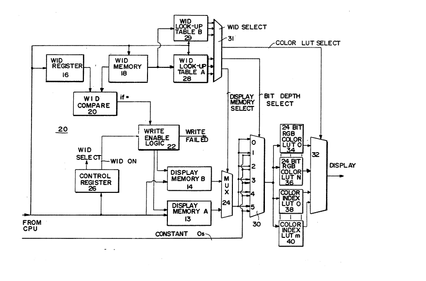
DETAILED DESCRIPTION OF ~E !NVENTlONi
Referring now to FIGURE 2 there is shown an improved computer oulput
system 20 based on the system 10 disclosed in FIGURE 1. The system 20
s includes double-buffered display memories 13 and 14 (also designated A and B)
which in the preferred embodiment may store twenty-four bits of information at
each position representing a pixel on the output display . These double-bufferedmemories 13 and 14 are especially useful in systems which provide animated
output to a display. The system 20 described in the present invention will,
0 however, operate as well with a single display memory.
The system 20 also includes a window identification (WID) register 16, a
window identitication (WID) memory 18, and a window identification (WID)
comparator 20 which operate in the manner described above with respect to
FIGURE 1 to control the writing of information to an appropriate window of a
cathode ray tube or other output device. As with the system 10 described in
FIGURE 1, the output of the window identification comparator 20 is furnished to a
write enable circuit 22 which provides signals for enabling either of the display
memories 13 or 14 depending on the information provided from a CPU (not shown
in FIGURE 2). A control register 26, is also included in the system 20 for
actuating the write enable logic 22.
The portions of the system 20 described to this point operate in essentially
the same manner as does the clrcuitry of the system 10 described above to
provide information from particular programs to particular windows on an output
display.
The system 20, however, includes in addition, a number of circuits which
allow it to perform in a substantially enhanced manner. First there is a WRITE
FAILED signal provided from WRITE Enable Logic 22 which indicates if any ot
the pixels have not been written because the Wl~ comparison failed. Such a
signal is useful for informing the software that a portion of a window has been
clipped so that the software may later deal with the clipped portion. Such a
signal may be stored by storage means well known to art and later utilized.
-8- Sun 82225.P050
,: , . . .
2~72~
The system 20 also includes a double buffered window identification (WID)
look-up tables 28 and 29 which are connected to receive signals from the
window identification memory 18 and the CPU. The signals received from the
window identification memory 18 are ~he four bit signals stored at each position5 representing each pixel of the display. Since four bit positions are utilized, each
such signal designates one of a possible sixteen individual windows or window
types for display at the output.
A WID select bit from control register 26 is used to select either WID look
. up table (A) 28 or WID look up table (B) 29 at any instant of time using multiplexor
10 31. The double buffering of WID look up tables allows the host to change the
; contents of one table while the other table is used for display output. Once the
window display attributes have been changed in the background WID look up
table, the CPU changes the WID select bit during the display vertical blanking
period. This provides the ability to change window display attributes without
5 disrupting the display.
Each of the window identification (WID) look-up tables 28 and 29 provides
three outputs. The first output is directed by the multiplexor 31 to the multiplexor
24 for controlling the selection of either display memory (A) 13 or display memory
' (B) 14~ The second output is directed by the multiplexor 31 to a multiplexor 30
20 which is utilized to select among a number of different color depths such as
twenty-four bit color information, twelve bit color information, or eight bit color
information. This same selection at multiplexor 30 can also be interpreted as
selecting a single buffer when the depth Is 8, 12, 24 bits between double buffers
when the depth is 8 or 12 bits, or between triple buffers when the depth is 8 bits.
25 The third output from the window identification look-up tables 28 and 29 is
directed, by the multiplexor 31 to a multiplexor 32 which selects among a numberof different color look-up tables for providing color signals to the output display.
The display refresh operation occurs when the read out of the contents of
the display memory is sent to the CRT output for display. The WID memory
30 contents are read out just like the display memory contents are read out during
the display refresh operation.
-9- Sun 82225.P050
..
" -.
,'
2 5
As explained above, in the preferred embodiment of the invention, the
window identification memory 18 stores four bits of information at each position to
designate the window number of a pixel on the output display. This four bits of
information allows sixteen individual windows or window types to be selected.
5 Each of those signals is furnished to lhe WID look-up tables 28 or 29 and causes
a particular set of outputs to be directed to the three multiplexors 24, 30 and 32 to
control the appearance of the display for that particular window. For example, afirst window to appear on a display might select the display memory 13 for the
storage of color information. This information is selected by that window number10 in the look-up tables 28 or 29 and causes a signal to be directed to the
multiplexor 24 to select the output from the display memory 13. Alternatively,
another window number might select display memory 14 and direct a signal to the
multiplexor 24 to select that display memory 14.
In the preferred embodiment of the invention as explained with respect to
15 FIGURE 1, a pair of display memories 13 and 14 are utilized in order to provide
double buffered output for rapid switching to the output display. This is useful in
. an arrangement which is utilized for animation purposes. In this preferred
embodiment of the invention, each of the display memories 13 and 14 provides
twenty-four bits of RGB color information at each position representing a pixel on
20 the output display. If twenty~four bits of color information are utilized, eight of
these bits provide red color information, eight of the bits provide green color
information, and eight of the bits provide blue color information. These are
furnished by the multiplexor 24 to a number of input terminals of the multiplexor
30. If the color depth of the window is twenty-four bits, the signal is furnished at
25 all of the inputs to the multiplexor 30, The data at the input labelled zero is
selected by the depth select output of the WID look-up tables 28 or 29 and
transferred by the output of the multiplexor 30 to a number of color look-up tables
34, 36, 38, and 40.
For many applications, however, twenty-four bits of color information are
30 not utilized. For example, some applications may utilize only twelve bits of RGB
color information while other applications utilize only eight bits of color
-10- Sun 82225.P050
.. , . . :
,
- . , . , .. , ~ .
- . : . . ~ - "
. 2,Qi~7~
information. This fact allows a single display memory to be utiiized for either
double or triple buffered output.
For example, if only twelve bits of RGB color information are utilized by a
particular application, this information when stored in one the display memories13 or 14 leaves an additional twelve bits of storage at each position which may
be utilized for a second frame of the same application. Presuming for example
that twelve bits of R~iB color information are stored in the twelve most significant
bits of the display memory 14, an additional twelve bits may be stored in the
twelve least significant bits at each position of the display memory 14. The
0 window look-up table 28 then provides indications by the depth selector input to
the multiplexor 30 to first select the twelve most significant bits as a first frame and
then to select the twelve least significant bits of the information at each position
as a second frame. These inputs to the multiplexor 30 are furnished at the
terminals labelled as 1 and 2. Consequently, first and second frames of a
particular application may be stored in the same display memory 13 or 14,
selected one after another by the depth selection output from the WID iook-up
table 28, and furnished to the multiplexor 30 for the particular window.
With each of the twelve bits of RGB color information at the input terminals
of the multiplexor 30, there is a second line provided to sach of the input
positions 1 and 2, a 12 bit pattern, in ths preferred embodimsnt, a constant string
of twelve zeros, to complete the necessary twenty~four bits of color informationwhich is necessary for ths color look-up tables 34; 36, 38, and 40.
The consequsncs of this ability of the system 20 is that a single display
memory 13 or 14 may bs utilized as a double buffered display memory by using
the first twelve bits at each position to represent a first frame of color information
and ths second tWslvs bits at sach position to represent a second frame of colorinformation. Conssquently, even though only a single display memory 13 or 14
is provided for ths system 20 in a particular embodiment double buffering may still
be accomplishsd.
In lik~ manner, certain applications utilized by the system 20 may be
adapted to perform with only eight bits of color information. In such a case, each
position of a display memory 13 or 14 may be utilized to store three distinct
- 11 - Sun 82225.P050
:.
- ~ ~
- .
~57~5
frames of color information which may be switched by means of ~he depth
selector output of the WID look-up tables 28 or 29 to the output of the multiplexor
30. In essence, when only eight bits of color information are utilized by the
application in the particular window, either of the display memories 13 or 14 is by
5 itself capable of providing triple buffered output. The inputs provided to themultiplexor 30 at positions 3, 4, and 5 then each carry eight bits of color
information. Along with' each eight bits of information, there is a sixteen bit pattern
provided, in the preferred embodiment, a sixteen bit constant of zeros to fill the
required twenty-four bits for transfer to the color look-up tables 34, 36, 38, and
:. 10 40 by the output of the multiplexor 30.
In the system 20 shown in FIGURE 2, the eight bits of input selected at the
input position 3 are the eight most significant bits, the eight bits of in?ut selected
at the position 5 are the eight least significant bits, and the eight bits of
information at position 4 are the intervening bits.
To recapitulate, the 0 input to the multiplexor 30 provides twenty-four full
bits of single buffered color information. The 1 and 2 inputs to the multip'3xor 30
each provide twelve bits of double-buffered RGB color information. The 3, 4, and5 inputs each provide eight bits of triple-buffered color information. It is, of course, not necessary that the display memories 13 and 14 be utilized to provide
20 double-buffering when utilizing twelve bits of color information or triple-buffering
when utilizing eight bits of color information. It is quite possible that any particular
application might utilize eight or twelve bits of color information yet provide only
single buffered output. If this is the case, the window look up table ~8 or 29
selects the individual input terminal to be utilized by the multiplexor 30 to provide
25 output to the color look-up tables.
Each of the outputs of the multiplexor 30 is handled differently by the color
look-up tables. In a complete twenty-four bit RGB color signal, eight of these bits
are utilized to indicate red, eight are utilized to indicate green, and eight are
utilized to indicate blue. These are transferred by the output of the multiplexor 30
30 to one of 0-N color look-up tables (indicated in FIGURE 2 as tables 34-36J, aplurality of color look-up tables provided by the system 20 for handling twenty-
four bits of RGB information. A particular window number provided to the WID
-12- Sun 82225.P050
. .
- ~ , ~ -.
-` 2~1572~
look-up table 28 or 29, for example, will select a particular one of the twenty-four
bit RGB color look-up tables to provide color output to the display.
These same twenty-four bit color look-up tables are utilized when only
twelve bits of color information are available and the remaining bit positions are
. 5 filled with zeros. In such a case, a particular color look-up table is provided with
the necessary values for each of the possible color signals available at the
` output of the multiplexor 30, and the window look-up table 28 or 29 provides via
- the multiplexor 31 the appropriate signal on the color look-up table select line to
the multiplexor 32 to select output from this particular color look-up table.
0 In a like manner, when a particular application utilizes only eight or twelve
bits of color information and the remaining bits are filled with zeroes, that
information is provided at the output of the multiplexor 30 and furnished to each of
the color look-up tables. The selection of the particular color look-up table to be
utilized is again made by the window identification look-up table 28 or 29 on the
15 color look-up table select line controlling the multiplexor 32. The color look-up
tables which operate with eight or twelve bits of color information are those tables
indicated as 38-40 which are further identified as color index look-up tables zero
through m in FIGURE 2. In the case of eight bits of color information, two hundred
fifty-six possible output combinations are provided by each of the color index
20 look-up tables zero through m. In the case of the twelve bits of color information,
four thousand ninety-six possible output combinations are provided by each of
the color index look up tables zero through m. The particular table selected
depends on the particular window in operation, the window number of which
causes the WID look-up table 28 or 29 to provide the appropriate signal on the
25 color LUT select line to control the multiplexor 32.
A special advantage of the present invention is that the window
identification look-up table 28 may be simply reprogrammed by signals from the
CPU to provide what amounts to, essentially, a new set of selection parametsrs
for the multiplexors 24, 30 and 32. By changing only a single bit within the
30 window identification look-up table 28, the CPU may provide for entirely different
selections of the display memories 13 and 14, of the depth of color information
-13- Sun 82225.P050
. . ~
7 ~ 5
provided by the multiplexor 30, and of the selection provided of color look-up
tables by the multiplexor 32.
This programmability allows a significant number of variations with the
system 20. For example, if a first application utilizes twenty-four bi~s of RGB
5 color, then the color look-up table zero (indicated as 34 in FIGURE 2) may be
utilized and selected by the color look-up table select output of the window
identification look-up table 28 by means of multiplexor 32. If, while operating with
that particular application, it is desired to change the colors available, then a
reprogramming of a single bit of the color look-up table 28 may cause a select
10 signal to be provided to the multiplexor 32 to select a different one of the twenty-
four bit RGB color look-up tables.
Moreover, an additional advantage of the present invention is that each of
the color look-up tables are programmable and thus may be varied by signals
from the CPU to provide additional cotor information beyond that available in a
15 fixed look-up table. For example, the CPU may provide signals to reprogram a
particular twenty-four bit RGB color look-up table one while the twenty-four bitRGB color look-up table zero is being utilized so that the color look-up table one
may immediately be chosen by means of the multiplexor 32 upon comPletion of
the present operation. Obviously, the same facility may be utilized to reprogram20 individual ones of the color index look-up tables zero through m (38-40)~ This
programmability provides for essentially an infinite variation in colors which may
be made available to any particular applicalion~ Such a provision is a
substantial improvement over fixed color look-up tables provided by the prior art~
Although the present invention has been described in terms of the
25 preferred embodiment, it will be appreciated that various modifications and
alterations might be made by the skilled in the art without departing from the spirit
and scope of the invention. The invention should therefore be measured in terms
of claims which follow:
-14- Sun 82225~P050
. .
, :
. : .