Note: Descriptions are shown in the official language in which they were submitted.
20157~
AE-338 PATENT
SHIELDED ELECTRICAL CONNECTOR
1 FIELD OF THE INVENTION:
This invention relates generally to an electrical
connector attachable to a printed circuit board and more
particularly relates to an electrical connector having a
metallic shield therearound which shields the connector from
electromagnetic and radio frequency interferences.
BACKGROUND OF THE INVENTION:
The benefits of providing a metallic shield around an
electrical connector have long been known. Electromagnetic
interferenee (EMI) and radio frequency interference (RFI) can
be redueed, if not eliminated, if a suitable shield is placed
around an eleetrical connector and connected to ground
potential to drain the interferenees to ground.
Many conneetors employ metallie shells or shields
therearound to effeetively provide such function. However,
many of these shields are bulky and must employ separate
hardware to seeure the shields to the eonnector.
In addition, many eonneetor applieations require that the
eonneetor be repeatedly inserted and removed from a mating
eonneetor housing where the mating eonnector housing has
eleetrieal eontaets therein whieh make ground eonneetion to the
eleetrieal shield to establish ground eontinuity between the
mating eonneetors. Often during repeated ey~eles of insertion
and removal, prior art eonneetion deviees have eneountered the
problem of the eonneetor shield dislodging from the eonneetor
housing. This is espeeially true where attempts have been made
to reduee the hardware neeessary to seeure the shield to the
housing~
Another problem eneountered in shielded eonnector
applications is that eertain of these eonneetors are supported
on a printed eireuit board. The eontaets extending from the
eonnector must be soldered to through-holes in the printed
eircuit board. The typieal soldering proeess may include
~'
201~7~
-2- PATENT
1 moving the connector and the printed circuit board through a
solder wave where it is subject to vibration. Again, it is
important that the shield be securely mounted to the connector
housing to avoid the possibility of the shie~d dislodging from
the connector housing during the wave solder process.
- It is desirable to provide a shielded electrical connector
where the shield of the connector is supported to the housing
without the use of additional mounting hardware and further
where the shield will be securely retained on the housing
regardless of soldering vibration or insertion and removal
stress.
; SUMMARY OF THE INVENTION:
It is an object of the present invention to provide an
electrical connector having a metallic shield therearound which
is securely retained on the housing of the connector.
It is a further object of the present invention to provide
a shielded electrical connector where the shield of the
connector is supported to the connector housing without the use
of additional securement hardware.
In the efficient attainment of these and other objects,
the present invention provides an electrical connector for
attachment to a printed circuit board. The connector includes
an insulative housing having a connection surface and an
attachment surface which is attachable to a printed circuit
board. Mounting ears extending from the housing provide a
securement member for securing the connector to the printed
circuit board. Plural electrical contacts are supported in the
housing having a connection end ad;acent the connection face
and contact tails extending through the attachment surface for
electrical engagement with through-holes of the printed circuit
board. The connector includes shielding means for shielding
the connector from electromagnetic and radio frequency
interferences. The shielding means includes first and second
planar shields along opposed longitudinal surfaces of the
connector housing. The first shield includes shield extending
... ... , .. . ..::
. .
20157~6
-3- PATENT
portions which overlie the mounting ears of the housing and the
second shield also includes shield extending portions having
extents which wrap around the mounting ears and overlie the
extending portions of the first shield. The arrangement of the
shield extending portions of the first and second shields
permit use of mounting hardware, normally associated with the
mounting of the connector housing to the printed circuit board,
to also secure the shield to the housing.
As shown by way of the preferred embodiment herein, the
connector further includes plural tabs spaced along the
longitudinal edge of first and second shield which extend
toward the insulated housing. The housing includes plural
slots spaced therealong which accommodate the tabs to
positionally confine the shield to the housing.
BRIEF DESCRIPTION OF THE DRAWINGS:
Figure 1 shows in perspective, the shielded electrical
connector of the present invention secured to a printed circuit
board shown in phantom and shown removed from its associated
mating electrical connector.
Figures 2 through 4 show top, front and bottom plan views
respectively of the shielded electrical connector of the
present invention.
Figure 5 is a partially fragmented sectional showing of
a mounting ears of the connector of the present invention.
DETAILED DESCRIPTION OF THE PREFERRED EM~ODIMENT:
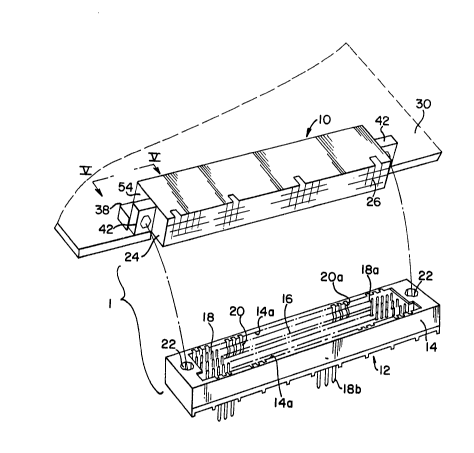
Referring to Figure 1 an electrical connection assembly
1 is shown. Connection assembly 1 includes a male shielded
electrical connector 10 and a mating female socket connector
12. Connectors 10 and 12 are designed for mating electrical
connection, with male shielded connector 10 being insertable
into female socket connector 12.
Female socket connector 12 is a conventional multi-pin
electrical connector including an elongate insulative housing
14 defining a central cavity 16 which accommodates in removable
~01~7~
-4- PATENT
1 disposition male shielded connector 10. Housing 14 supports
a plurality of electrical contact pins 18 having upper portions
18a extending into cavity 16 and opposed lower portions 18b
extending exteriorly through housing 14. Housing 14 also
supports a plurality of additional electrical contacts 20 along
the interior sidewalls 14a thereof. Electrical contacts 20 are
spring type contacts having upper spring portions 20a which
; extend into cavity 16. As will be described in greater detail
hereinbelow, contact pins 18 are designed for electrical
connection with mating contacts of male shielded connector 10
while electrical contacts 20 are designed for connection with
the shielded portions of male shielded connector 10. Housing
14 further includes at the ends thereof, mounting apertures 22
which receive appropriate hardware (not shown) to secure male
shielded connector 10 to female socket connector 12.
With additional reference to Figures 2 through 4 male
shielded connector 10 of the present invention may further be
described. Shielded connector 10 includes an elongate
insulative housing 24 having a generally rectangular shape and
structured to be accommodated in the cavity 16 of female socket
connector 12. Housing 24 includes a connection surface 26
along one longitudinal side thereof and an attachment surface
28 (Fig. 4) along another longitudinal side thereof.
In the particular embodiment shown in the present
invention, connection surface 26 is disposed in a plane which
is perpendicular to the plane containing attachment surface 28,
to form what is known in the lndustry as a right-angle
connector. As attachment surface 28 is secured to a printed
circuit board 30, shown in phantom in Figùre i. In the present
invention, connection of male shielded connector 10 to female
socket connector 12 is made in a direction parallel to the
plane of the printed circuit board 30. It is, however,
contemplated that the present invention may be practiced in a
straight-through connector, that is, a connector having a
connection surface and an attachment surface in spaced parallel
orientation.
,
.. .. .: - :. ::
2~ ~7~
-5- PATENT
Male shielded connector 10 further includes a plurality
of electrical terminals 32 (Figs. 3 and 4) in like number to
the number of contact pins 18 in female socket connector 12 for
electrical connection therewith. Terminals 32 are of the
right-angle variety having a connection portion 34 disposed at
a right-angle to a terminal tail 36. As shown in Figure 3 in
~; preferred embodiment, connection portion 34 of terminal 32 is
; formed into a conventional socket for electrical engagement
- with the contact pins 18 upon insertion of male shielded
- 10 connector 10 i~t~ female socket connector 12. However, other
conventionally formed terminal shapes may be employed.
i Connection portions 34 of terminals 32 are positioned along
connection surface 26, to facilitate interconnection with
contact pins 18. Terminal tails 36 extend beyond attachment
surface 28 to make electrical interconnection with plated
` through-holes (not shown) of printed circuit board 30.
In order to positionally secure male shielded connector
10 to printed circuit board 30, male shielded connector 10
includes board mounting ears 38 extending from each transverse
end thereof. As shown in more detail in Figures 2 and 4, board
mounting ears 38 extend outwardly from housing 24 and include
a central aperture 38a alignable with like apertures (not
shown) on printed circuit board 30. A conventional nut and
bolt assembly 40, shown more specifically in Figure 5, may be 25 used to secure male shielded connector 10 to printed circuit
board 30.
Male shielded connector 10 further includes connector
mounting ears 42 adjacent each o$ board mounting ears 38.
Shown more speci$ically in Figure 3, connector mounting ears
42 include a central aperture 42a alignable with mounting
apertures 22 of female socket connector 12 so that a fastening
device (not shown) may be inserted therethrough to secure male
shielded connector 10 to female socket connector 12.
In order to shield male shielded connector 10 from
electromagnetic interferences (EMI) and radio frequency
interferences (RFI), connector 10 includes shields 50 and 52
~ .
- . ,:'
.
201~7~
-6- PATENT
1 along housing 24. Each of shields 50 and 52 is an elongate
substantially planar member formed of an electrically
conductive material, preferably metal~
Re~erring to Figures 2 and 5, shield 50 is disposed on an
upper longitudinal surface 44 of housing 24. Shield 50
includes a planar portion 51 partially coextensive with upper
surface 44. A depending portion 54 extends downward toward
each board mounting ear 38. Shield 50 further includes a
projecting portion 56 which extends over an upper surface 37
f board mounting ear 38. An opening 56a is alignable with
aperture 38a of mounting ear 38.
Referring Figures 4 and 5, lower shield 52 is positioned
along attachment surface 28 of housing 24. Shield 52 includes
a planar portion 57 which is partially coextensive with
attachment surface 28, however, having a cutaway portion 52a
permitting passage of terminal tails 36 therethrough. A pair
of opposed lateral extents 58 extend over a lower surface 39
of board mounting ears 38. Each lateral extent 58 includes an
opening 58a therethrough alignable with the aperture 38a of
board mounting ears 38. Lateral extents 58 further include
upstanding side portions 60 which extend upward toward upper
shield 50. A distal end extent 62 extends at a right angle to
side portion 60 over the projecting portion 56 of upper shield
50. An opening 62a in distal end extent 62 is alignable with
opening 56a of projection portion 56 of shield 50 and also
alignable with aperture 38a of mounting ear 38. The lateral
extent 58, upstanding side portion 60 and distal end extent 62
actually wrap-around shield ear 38 and projecting portion 56
of shield 50, to partially enclose projecting portion 56 and
shield ear 38.
As is clearly depicted in Figure 5, providing a shield
formed in such fashion permits nut and bolt assembly 40 not
only to secure housing 14 to printed circuit board 30 but also
to secure each of shield 50 and 52 to housing 14. Thus,
mounting hardware normally associated with the securement of
male shielded connector 10 to printed circuit board 30 may also
20157~
--7--
l be used to secure the metallic shields 50 and 52 to the
connector housing 14. ~ny vibratory forces which may be
encountered will not cause the shields 50 and 52 to be
dislodged from housing 24, as the nut and bolt assembly 40
securing male connector 10 to printed circuit board 30 also
sec~res the shields 50 and 52.
Referring again to Figures 1 through 4, shields 50 and 52
are additionally secured to housing 24 along the longitudinal
`~ edges thereof adjacent connection surface 26. Each of shields
;. 10 50 and 52 includes plural inwardly projecting tabs 70 whichproject into housing 24. As shown in Figures 2 through 4 each
¦ of shields 50 and 52 includes four such tabs 70 spaced
longitudinally thereacross which are punched from the planar
portions 51 and 57 of the respective metallic shields 50 and
52. Housing 24 includes plural slots 72 (co-extensive with
tabs 70 as shown in Fig. 3) adjacent connection surface 26
which receive each of tabs 70. The arrangement of the tabs 70
and the slots 72 serve to securely position each of shields 50
; and 52 with respect to housing 24. Thus, upon repeated
insertion and removal of male shielded connection 10 with
female socket connector 12 ~Fig. 1) the shield will remain
securely in place with respect to housing 24.
Z Various changes to the foregoing described and shown
structures wou~d now be evident to those skilled in the art.
Accordingly, the particularly disclosed scope of the invention
is set forth in the following claims.
3o
:. .
~,