Note: Descriptions are shown in the official language in which they were submitted.
` 2~157~7
AE-324 PATENT
TOOL FOR SEMICONDUCTIVE CHIP REMOVAL
1 FIELD O~ T~E INVENTION:
This invention relates generally to devices for the
removal of semiconductive chips from chip carriers and pertains
more particularly to improved devices providing removal of
chips from chip carriers which are secured to printed circuit
boards.
' BACKGROUND OF THE INVENTION:
For many years, microprocessors and like computer
apparatus have been configured with printed circuit boards
(PCBs) having semiconductive chip carriers or receptors secured
thereto, with semiconductive chips releasably secured in the
chip carriexs. The chips have a generally rectangular array
of male contacts depending therefrom and the chip carriers are
configured with female contacts at their upper side for the
receipt individually of the chip-dependent male contacts.
j The chip carriers are further configured with male
contacts electrically continuous with their female contacts
and the former are inserted in PCB conductive strip apertures
and then "free-flow" soldered thereto. The free-flow soldering
provides electrical continuity from the chip male contacts to
jthe PCB traces and also provides the full basis of mechanical
securement of the chip carrier to the PCB.
There occurs need for the removal of chips from chip
carriers, for various reasons, such as chip failure, and the
art has seen various tools for this purpose; the function of
the tools evidently being to impart uplifting force to the chip
to overcome the engagement, ~rictional force pre-existing as
between the chip male contacts and the chip carrier female
contacts. This is a substantial frictional retention force to
overcome since the chip male contact array can include a
hundred or more individual contacts.
.
' ;'. ... ;.. ~ .
201~7~7
--2--
1 The prior art efforts in the chip tool removal field have,
to applicants' considerations, not sufficiently met the
industry requirements, particularly with respect to the
integrity of elec~rical connection of the chip carrier and the
PCB. Thus, the prior art tools operate in manner imparting
forces as between the interface of the chip carrier and the PCB
and may adversely effect the electrical connection thereof,
which is fundamental to the electrical interconnection of the
replacement chip and the chip carrier.
SUMMARY OF THE INVENTION:
The present invention has as its primary object the
provision of improved tools for the removal of chips from chip
carriers secured to PCBs.
1~ A more particular object of the invention is the provision
of chip removal devices the operation of which may impact less
adversely on the electrical interconnection interface between
the chip carrier and the PCB than heretofore known devices of
this character.
In attaining the foregoing and other objects, the
invention provides a chip removal tool which includes mutually
displaceable removal members bearing respectively against an
exteriorly-accessible surface of the chip and against an
exteriorly-accessible surface of the chip carrier, neither of
such removal members bearing on the PCB in the course of chip
removal.
More particularly, the invention provides apparatus for
effective removal of a semiconductive chip having an
exteriorly-accessible surface and chip contacts depending
therefrom from a chip carrier having an exteriorly-accessible
surface and chip receptor contacts therein in retentive
engagement with the chip contacts. The apparatus comprises a
chip-bearing platen having first arms extending therefrom for
engagement with the chip exteriorly-accessible surface to bear
thereon, and a chip carrier-bearing platen having second arms
extending therefrom for engagement with the chip receptor
. , . , , ~
20~7~7
--3--
1 exteriorly-accessible surface to bear thereon. The first arms
extend through and beyond th~ chip carrier-bearing platen and
the first and second arms each define bearing elements for
common disposition between the exteriorly-accessible surfaces
of the chip and the chip receptor. The platens are arranged
for translation relative to one another, whereby the bearing
elements are mutually displaced, effecting removal of th~ chip
from the chip carrier. In particularly shown form, the
apparatus includes operator-controllable handles for effecting
displacement of the platens.
The apparatus is preferably adapted for use with diversely
sized chips and chip carriers and hence is shown as further
including operator-controllable members for effective
displacement of the first and second arms relative to one
another in a further direction, i.e., widthwise of the chip and
carrier, to adapt the apparatus to diversely-sized chips and
chip carriers. This feature also permits the operator to more
easily attached the apparatus to the chip carrier.
The foregoing and other objects and features of the
invention will be further understood from the following
detailed description of preferred embodiments of the invention
and from the drawings wherein like reference numerals identify
like parts and components throughout.
3RIEF DESCRIPTION OF THE DRAWINGS:
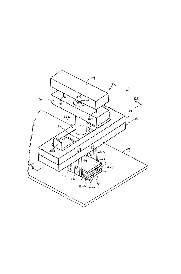
Figure 1 is a perspective illustration of a preferred
embodiment of a tool constructed in accordance with the
invention, shown in its state of having removed a chip from a
chip carrier.
Figure 2 is an exploded front elevational view of the
several separate components of the tool of Fig. 1, broken apart
and sectioned in part for showing of interior detail.
Figure 3 is perspective illustration of the interior
mechanisms of the chip-bearing platen and the chip carrier-
bearing platen of Fig. 1 as seen from plane III-III thereof.
.
.
201~757
--4--
1 DETAILED DESCRIPTION OF THE PREFERRED EMBODIMENT:
Referring to Fig. 1, a semiconductive chip 1 has an
exteriorly-accessible surface 2 and chip contacts 3 depending
therefrom. A chip carrier or chip receptor 4 has contact
sockets 5 for receiving ~ontacts 4 and is itself soldered in
place with its dependent contacts 6 in electrical communication
with electrically conductive traces (not shown) of printed
circuit board (PCB) 7. Chip carrier 4 has exteriorly-
accessible surface 8. While a semiconductive chip 1 and
accompanying chip carrier 4 is shown, the invention may also
be employed with other types of electrical devices and
associated connectors.
Tool 10 of Fig. l, shown in operated relation, having
removed the semiconductive chip from the chip receptor,
includes an upper mechanism comprising operator-controllable
handle unit 12 with an upper handle 14 and a lower handle 16,
guides 18 and 20 controlling handle relative movement as for
directionality.
Shaft 22 is secùred to handle 14 and follows movement of
handle 14 as an actuator, as is more fully discussed below.
Spring 24 biases handles 14 and 16 into normal, vertically
spaced, relation. Handle 16 has actuator shaft housing 26
fixedly dependent there$rom And in engagement with chip-bearing
platen assembly 28, which includes platen 30 and depending arms
32 and 34.
Chip carrier-bearing platen assembly 36 includes platen
38 and depending arms 40, 42, 44 and 46. Width adjustment keys
48 and 50 (Fig. 2) are spring-biased oùtwardly relative to
housing 26 by structure covered in detail hereinafter. The
keys are moved by a user toward housing 26 and respectively
operate on arms 34, 44 and 46 and arms 32, 40 and 42,
displacing the former rightwardly and the latter leftwardly in
Fig. 1.
In the course of reaching the Fig. 1 tool-operated state,
an outset step involves the movement of keys 48 and 50 to
dispose the platen arms outwardly of the sides of the chip
. , " " , . ., . , " ~ ,
: - ~ : ~:- , -
2015757
--5--
1 and chip carrier. Next, with the bearing elements of the
platen arms in respective alignment (Fig. 3), the keys are
released and the bearing elements move under spring bias into
the interstice existing ~etween the assembled chip and carrier,
i.e., the space between the chip ~ndersurface and the carrier
oversurface. Thereupon, handles 14 and 16 are pressed toward
one another, effecting upward displacement of the chip relative
to the chip carrier and removal of the chip from the carrier.
of significance, alluded to above, is that no part of tool
10 bears contiguously upon PCB 7 in the course of the chip
removal operation. Thus, once the tool is applied to the chip
and carrier, the soldering interface between the carrier and
the PCB is isolated from the removal operation.
The components of tool 10 are seen in exploded manner in
Fig. 2, wherein handle assembly 12 is shown rotated ninety
degrees from its Fig. 1 disposition relative to platen
assemblies 28 and 36. For this purpose, handle 16 may be
rotatively secured to housing 26, with suitable keying to
secure the handles in desired Fig. 1 orientation and to release
them for movement into the Fig. 2 orientation, the former
adapting the tool to the human hand for joint operation of keys
48 and 50 and handles 14 and 16, and the latter facilitating
packing and storage of the tool.
In Fig. 2, it is seen that housing 26 has a threaded end
26a, actuator shaft 22 having extent to expose its end 22a
below housing end 26a. Shaft end 22a is open and interiorly
threaded for the receipt of a securing screw 22b. Handle
assembly 12 is joined to platen assembly -28 by threading
housing end 26a into interiorly-threaded bore 52, which extends
fully through central piece 30a of platen 30.
The sets of platen arms shown in Fig. 2 will be seen to
be in vertical alignment, e.g., arms 32 and 42 are aligned, as
would also be ~rm 40, and arms 34 and 46 are aligned, as would
also be arm 44. Passages 54 and 56 are formed through platen
38 to permit travel of arms 32 and 34 therethrough, beyond
` 201~7~7
--6--
1 central piece 38a, into registry respectively between arms 40
and 42 and between arms 44 and 46, as is depicted in Fig. 1.
In the course of this last described tool assembly step,
shaft end 22a becomes resident in counterbore 58 of piece 38a
of platen 38. At this stage, screw 22b adapted to bear on the
undersurface of platen 38, is threaded into shaft end 22a, thus
securing the collective assembly of handle assembly 12, platen
assembly 28 and p~aten assembly 36.
Operation of handles 14 and 16, by pressing them together,
will now be seen to give rise to displacement of chip-bearing
platen 30 upwardly relative to chip carrier-bearing platen 38
by bearing elements 32a and 34a, platen 38 being maintained in
force relation with shaft end 22a and the oversurface of the
chip carrier by bearing element 42a and its unshown counterpart
on arm 40 and bearing elements 44a and 46a.
As is seen in Fig. 3, all of the bearing elements have
common plane disposition in a first or unoperated state of the
tool and, as is shown in Fig. 1, occupy vertically spaced
planes in the operated state of the tool. The invention
contemplates the provision of recesses, such as are shown at
4a in Fig. 1, configured for the ready receipt of the bearing
elements at the chip and chip carrier interstice.
The interior mechanisms of platen assemblies 28 and 36
are shown in Fig. 3, with the central rigid pieces 30a and 38a
of the assemblies, cross-hatched in Fig. 2, omitted for clarity
of illustrating such mechanisms. Referring to Fig. 3, key 48
controls the movement of frame 60 and key 50 controls the
movement of frame 62. Frame 60 has cross-member 64 at its
rightward end, supporting arm 34. Springs 66 and 68,
schematically shown, are disposed between cross-member 64 and
cross-member 70 of frame 62. Block 72 is fixedly positioned
and bears against cross-member 70.
Frame 62 has end cross-me~ber 74 and springs 76 and 78
are disposed between cross-member 74 and cross-member 80 of
- ~ . . , . ,~ . .
2~1~7~7
--7--
1 frame 60. Block 82 is fixedly positioned and bears against
cross-member 80. As will be seen, rightward displacement of
key 48 displaces cross-member 64 and hence arm 34 rightwardly,
against the bias of springs 66 and ~8. Leftward displacement
of key 5~ displaces cross-member 74 and hence arm 32
leftwardly, against the bias of springs 76 and 78. The rest
positions of the keys is as indicated, against the fixed blocks
72 and 82.
; The mechanism interiorly of platen assembly 36 includes
lOsupport 84 for arms 40 and 42, fixed block 86 and springs 88
, and 90 urging support 84 away from block 86. Support 92 has
arms 44 and 46 extending therebelow. Fixed block 94 and
springs 96 and 98 urge support 92 into its illustrated rest
position. As cross-members 64 and 74 are displaced, supports 15 84 and 92 follow their movements under the influence of springs
88, 90, 96 and 98.
Various changes may be introduced to the foregoing tool
configuration and modifications may be made in the described
method of its operation and use without departing from the
invention. The particularly described and discussed embodiment
and methods are thus intended in an illustrative and not in a
limiting sense. The true spirit and scope of the invention are
set forth in the following claims.
.. - ... ~