Note: Descriptions are shown in the official language in which they were submitted.
201S853
10577-201/T18
LINEAR ARRAY WAFER SCALE INTEGRATION ARCHITECTURE
BACKGROUND OF THE INVENTION
This invention is directed to an architecture
for interconnecting an array, and in particular to use
of that architecture to construct a linear array from a
wafer scale integrated array of substantially identi-
cally formed cells.
Since commercial introduction of integrated
circuitry, there has been a continuing trend toward
putting more and more circuitry onto smaller and smaller
areas of integrated circuit chips. One reason for this
trend is to reduce the number of chip-to-chip connections
which tend to reduce circuit speed, introduce noise,
and often cause reliability problems due to mechanical
failure. Another reason is the requirement for driver
circuits when signals are brought off-chip - at the
expense of circuit area. There are also economic con-
siderations: A system developed from multiple chips
encounters higher packaging and manufacturing costs
than if implemented in fewer (or, ideally, one) chips.
On the other hand, as the circuit size
increases, fabrication flaws tend to reduce the yield
of useable circuits from a wafer.
It is not too surprising, therefore, to see
that very large scale integration (VLSI) is turning to
wafer scale integration, as a response to the increas-
ing demand for higher integrated circuit density. Waferscale integration provides a large density advantage
over VLSI.
Wafer scale integration seeks to assemble an
entire system on a single wafer, rather than partition
the wafer into chips that each carry smaller portions
of a system, and thereby requires the expense of indi-
vidual packaging. However, yield has been one problem
20~5853
that works against successful wafer scale integration.
Fabrication flaws must be overcome in order to effec-
tively and economically use wafer scale integration
techniques.
There are a number of wafër scale techniques
known today aimed at overcoming the yield problem. One
such technique utilizes redundant copies of a digital
system formed on a wafer, and provides selection cir-
cuitry integrated in each of the systems. The selection
circuitry intercouples portions of each copy of the
system in a manner that results in one, flaw-free, work-
ing version of the desired digital system. An example
of this technique can be seen in U.S. Pat. No. 4,621,201.
Another approach, and one to which the present
invention is directed, involves forming a multiplicity
of substantially identical-circuits or cells on a wafer.
Each cell contains logic for performing one or more
functions (e.g., arithmetic and/or logic functions,
memory functions, or any combination of these~and other
functions). Various techniques are then used for inter-
connecting these-cells. ~
Among the different connection techniques
known today are (1) imbedding the cells in a sea of
switches to interconnect them in various fashions (i.e.,
to form 2-D meshes, linear arrays, tree configuration,
and the like) using fuses or switches that are set during
manufacture; or (2) interconnecting the cells with cross-
bar switches, connecting every pair of cells. Examples
of these kinds of wafer scale integration formations
can be seen in W.R. Moore, "A Review of Fault Tolerant
Techniques for the Enhancement-of Integrated Circuit
Yield," Proc. of the IEEE, Vol. 74, May, 1986, pp. 684-698;
W. Chen, et al., "A WSI Approach Towards Defect/Fault
Tolerant Reconfigurable Serial Systems," IEEE Journal
of Solid State Circuits, Vol. 23, June, 1988, pp. 639-646;
J. Trilhe and G. Saucier, "WSI - The Challenge of the
Future"; Proc. IEEE Conference on VLSI and Computers,
20~8S3
May, 1987. these interconnecting techniques can tend
to use more wafer area, create more complex circuitry,
and pose a routing problem for signal lines.
Yet another, more simplified approach, is to
have bidirectional busses connecting each rectangular
cell to its four adjacent neighbors. The input to the
cell is selected from one of the four neighbors, and
the output driven to a different neighbor. The main
problem with such a structure is that every cell must
have two operating neighbor cells in order to be included
in a linear array or "chain" of such cells. Also, it
is difficult to configure a chain in such a way that
both the beginning and end are on a wafer periphery
where they may be connected to bonding pads.
A more practical cell interconnection approach
has been to provide separate inputs and outputs between
a cell and each of its neighbors to increase interconnec-
tion flexibility. In this approach, the cell carries a
logic function whose input may be selected from any one
of the four neighbors, and whose output is, in turn,
communicated to the selection logic associated with
each boundary (which also receives inputs from each of
the other boundaries). Although this structure provides
sufficient paths to connect around many defective cells,
there are several drawbacks: The delay between the
logic functions of any two cells depends upon the number
of individual selection logic elements between them.
Since this is not known at the outset, the delay is
unbounded. Also, the amount of logic to implement the
selection logic (e.g., multiplexers) may take up a sig-
nificant area of the cell, and particularly so when the
information is communicated in parallel instead of bit
serial form. Further, the routing of the necessary
signal lines tends to be irregular and confused; since
every side must connect to every other side, it is pos-
sible that interference with logic routing lines will
be encountered. Further still, it is difficult to find
20~58S3
an acceptable configuration algorithm that allows connec-
tion to any reachable cell. This and similar struc-
tures are discussed in T. Leighton and C.E. Leiserson,
"Algorithms for Integrating Wafer Scale Systolic Arrays,"
Systolic Signal Processing Systems, Dekker, 1987, pp.
299- 326; M.J. Shute and P.E. Osman, "COBWEB - A Reduc-
tion Architecture," Wafer Scale Integration; Adam Hilger,
1986, pp. 169-178; and M.G.H. Katevenis and M.G. Blatt,
"Switch Design for Soft-Configurable WSI Systems"; Proc.
IFIP Int l Workshop on WSI, Elsevier Science Publishers,
1986, pp. 255-270.
A modification of the foregoing approach is
implemented in a wafer-scale integrated memory system.
Each cell carries a pair of shift registers that are
used, when connected to neighbor cells, to form a-spiral,
consisting of a single, long shift register chain. The
first half of the path through the shift register chain
is formed by one of the shift registers of each cell;
the return path contains the second shift register of
each cell. There are two inputs to the cell from each
neighbor cell; one input (from each neighbor) is multi-
plexed to the input of one of the shift registers, the
other input (from each boundary) to the other shift
register. In similar fashion the outputs~of each shift
register are multiplexed to one of two outputs to each
neighbor. While this scheme may simplify the multiplex
circuitry used in the connection techniques discussed
above, it still requires more than is believed needed.
Further, known implementations of the approach use a
cell-to-cell connection scheme that lacks flexibility,
resulting, it is believed, in a less than optimum harvest
of those cells available for inclusion in the chain.
(As used herein, "harvest" is used to refer to those
cells that are actually included in any interconnection
of the cells, relative to the number of cells on the
wafer that operable.) An example of this approach is
found in U.S. Patent No. 3,913,072.
2.o 1~8~3
There have been also approaches that have amplified
the aforementioned basic structure, adding connections to
additional neighbours thexagonal arrays - see M.J. Shute,
supra) or neighbours that are not edge-adlacent (i.e., corner
neighbours). These designs, however, tend to suffer from the
same general problems as the rectangular approach, both offer
some increased harvest at the expense of extra cell area and
layout difficulties.
SUMMARY OF THE INVENTION
In accordance with the present invention there ls
provided a cell structure suitable for use in a cellular
array, the cell being formed to have N boundaries, each
boundary having an input bus means and an output bus means for
respectively communlcatlng signals lnto and out of the cell,
each boundary being located between a flrst ad~acent boundary
and second adjacent boundary, the cell structure comprising:
selection means associated with each boundary and having
plural selection inputs, coupled to receive the input bus
means and the output bus means of the associated boundary, and
a selection output, the selection output associated with
N - 1 of the boundaries being coupled to the output bus means
of the corresponding first ad~acent boundary, the selection
means being operable to select between the lnput bus means and
the output bus means; logic means coupled between an output of
the remaining one of the N selection means and the output bus
means of the corresponding first ad~acent boundary, the logic
means being configured and constructed to perform logic
functions; and control means operably coupled to each of the
s
.~
64157-322
,~o 1 5~ 53
selectlon means for causing at each selection means selection
of one of the plural selection inputs.
In accordance with the present invention there is
also provided a plurality of integrated circuit cells of
substantially identical construction formed on a semiconductor
wafer, each of the cells being formed to have N boundaries,
each boundary having input and output bus means for
respectively receiving signals thereat and first and second
adjacent boundaries, the integrated circuit cells each further
comprising plural selectlon means, each associated with a
corresponding one of the boundaries, and having at least a
pair of selection inputs coupled to receive the input bus
means and the output bus means of the associated boundary, and
a selection output, the selection means being operable to
select between the input bus means and the output bus means
for communication to the selection output; logic means coupled
between the selection output of a one of the selection means
and the output bus means of a boundary ad~acent the boundary
with which the one selection means in associated, the
remaining selection means having their selection outputs
coupled to the output bus means of the boundary ad~acent to
the boundary associated with such remaining selection means,
the logic means being configured and constructed to perform
logic functions; and control means operably coupled to each of
the selection means for causing at each selection means
selection of one of the plural selection inputs.
In accordance with the present invention there is
further provided apparatus formed on a wafer of semiconductor
. ~
64157-322
~ ~ 1 5~
material, the apparatus comprising an array of substantially
identlcally conflgured cells contalnlng loglc clrcultry, the
array contalnlng periphery cells defining the periphery of the
array, and interior cells definlng the remalnlng cells of the
array, each of the cells having at least one neighbour cell
ad~acent thereto, each of the cells further comprislng a
boundary between the cell and each nelghbour cell adiacent
thereto; lnput and output bus means assoclated wlth each
boundary for comMunlcating signals from and to the neighbour
cell ad~acent the correspondlng boundary, respectively;
selection means for communicating signals from the input bus
means associated with a selected one of the boundaries to the
logic circuitry; means for communicating output data signals
from the logic circuitry to the output bus means associated
with a one of the boundaries, and to the selection means
associated with the one boundary; the selection means
including means for receiving the output data signals from the
logic circuitry and for communicating the output data signals
to the output bus means associated with other of the
boundaries; and whereln each cell of the array is formed on
the wafer rotated 180 degrees relative to any neighbour cell
thereto.
The present invention provides a simplified
architecture that is adaptable for use in connecting an array
of digital systems to form there from a linear array of such
systems. The invention is particularly applicable for use in
wafer scale integration having formed thereon an array of
cells, interconnecting the cells in a linear array. When used
6a
64157-322
lolS ~53
in wafer scale lntegration, the archltecture uses lntercon-
nectlon or conflguratlon loglc lmplemented ln less clrcultry,
and thereby uses less wafer space, than presently known.
Accordlng to a preferred lmplementatlon of the
present lnventlon, when used ln connectlon with a wafer scale
lntegratlon of an array of cellsr each cell ls identically
structured, and has N boundarles. Each boundary ls provlded
wlth an lnput and an output bus structure for respectlvely
recelvlng slgnals from, and providing signals to, the
nelghbour cell ad~acent the boundary. Configuratlon loglc,
includlng N selection clrcults, one for each boundary,
provldes a palr of inputs coupled to recelve and select
between the input and output bus structure of the boundary.
N-l of the selectlon clrcults operate to communlcate the
selectlon to the output bus structure of the boundary ad~acent
that with whlch the selectlon clrcultry is assoclated. The
remaining (Nth) selectlon clrcult communlcates lts selectlon
lnput to a loglc functlon clrcuit whlch contalns the func-
tlonal loglc of the cell. The output of the loglc function
clrcult connects to the output bus structure of the ad~acent
boundary.
The loglc function clrcuit lncludes control for each
of the selectlon clrcults, recelvlng slgnalling from each of
the adjacent cells to, in effect, open that cell to such
adiacent cell.
The cell architecture of the present inventlon ls
preferably orlented, when used to form a wafer scale
lntegrated circult, so that the cells are arranged wlth thelr
6b
64157-322
~ lS~ 5~ .
opposlte sides rotated 180 degrees relative to any ad~acent
cell. A slmple conflguratlon algorlthm ls then used to
loglcally connect the loglc functlons of the cells to one
another uslng the selectlon clrcults ln a llnear array.
In the preferred ernbodlment of the lnvention, each
cell ls formed on the wafer so that lt ls generally
rectangular ln shape, thereby provldlng each cell wlth four
boundarles and four nelghbours (except those at the perlphery
of the wafer). Assoclated wlth each boundary ls a two-to-one
multlplexer that ls connected to receive the input bus from,
and the output bus tol the cell at the assoclated boundary.
Three of the multlplexers have thelr respectlve outputs
connected to the output bus of the ad~acent boundary clockwise
from that of the multlplexer. The output of the fourth
multlplexers ls also coupled to the ad~acent output bus, but
vla the functlon loglc carrled by the cell.
The conflguratlon logic of each celll upon power-up,
places the multlplexers ln a selectlon mode that forms a
closed-loop data path. Access to any cell can be lnltlated by
any nelghbour cell by assertlng an OPEN slgnal, causlng the
multiplexer associated wlth the boundary to the nelghbour to
select the correspondlng lnput bus. Once access ls made, the
clrcultry contained by the cell may be tested, and that cell
then used to
~- 6c
.~,
64157-322
2~58S3
_ 7
gain access to one of its neighbors. In this manner a
linear array or chain of cells is formed.
A number of advantages flow from the cell
architecture of the present invention. First, as indi-
cated above, the circuit delay from cell to cell (ormore accurately, from function logic of any one cell to
the function logic of an immediately adjacent cell in
any formed chain) is no longer unbounded; it is essen-
tially four multiplexer delays per function logic.
In addition, the cell architecture of the
present invention reduces the amount of logic in the
signal path of the chain by being able to use a more
simplified multiplexer than that proposed by the prior
art. The present cell architecture requires only a
two-input multiplexer, whereas prior art techniques
have often proposed five-input multiplexers (for a four
boundary cell) and more inputs are needed when addi-
tional boundaries are proposed.
Intercell connections are less complex with
the cell architecture of the present invention, resulting
in less signal lines (for signal communication) and
more simplified circuit layouts.
Linear array configuration using the archi-
tecture of the present invention is greatly simplified.
These and other aspects and advantages of the
present invention will be readily appreciated by those
skilled in the art upon reading of the following descrip-
tion of the preferred embodiment, which should be taken
in conjunction with the accompanying drawings.
BRIEF DESCRIPTION OF THE DRAWINGS
Fig. 1 is a simplified block diagram of the
cell architecture of the present invention;
Fig. 2 is an illustration of an array of cells
formed according to the teachings of the present inven-
tion in wafer scale integration;
~ 1 5g ~3
Fig. 3 is a simpllfled block dlagram to illustrate
the preferred method of communicatlng a clock signal to the
cells formed in accordance with the teachings of the present
inventlon,
Fig. 4A illustrates configuratlon latches used ln
the present lnventlon;
Fig. 4B ls a dlagrammatic array of four cells
constructed ln accordance with the present lnvention to
illustrate sequential logic lnterconnection of cells by a
simple configuratlon algorithm;
Fig. 4C is a flow chart illustrating, in simplified
form, the ma~or steps taken to configure a linear array of
cells constructed in accordance with the teachlngs of the
present lnventlon;
Fig. 5 illustrates use of the present invention in
combination with a memory system; and
Fig. 6 illustrates the circuitry used to open a
boundary between two cells constructed as illustrated in Fig.
1.
DESCRIPTION OF THE PREFERRED EMBODIMENT
CELL ARCHITECTURE
Turning now to the Figures, and for the moment
specifically Fig. 1, there is illustrated in simplified, block
diagram form a cell, designated generally with the reference
numeral 10, constructed in accordance with the teachings of
the present invention. As illustrated, the cell 10 is
rectangular in shape, having four boundaries labelled North
(N), West (W), South (S), and East (E). (As used here,
64157-322
~vl5~53~
boundaries refers to the edge portions of the periphery of a
cell shared with a nelghbour cell.) Associated wlth each of
the boundarles N, W, S, and E are 2-to-1 multiplexers 12N,
12W 12S, and 12E, respectlvely. Also associated wlth each of
boundaries N,...,E are input and output busses IN-X and OUT-X,
respectively (where X is the deslgnatlon of the partlcular
boundary N,....,E). Each of the IN and OUT busses of the cell
10 connect to a correspondlng OUT and IN bus of an ad~acent
cell. Thus, for example, the cell 10W, partially lndlcated ln
phantom on the boundary E of cell 10 has lts correspondlng
output and lnput busses (located at what would be boundary E
of the cell lOW), OUT-E' and IN-E' respectlvely connected to
the IN-W and OUT-W busses of the cell 10. That ls, the OUT
and IN busses of a cell correspond to the IN and OUT buses,
respectively, of a neighbour cell at any one boundary.
It should be noted at thls polnt that the IN and OUT
busses can be structured to convey lnformatlon ln bit-serlal
format or multi-bit format. The advantages of the present
invention permit information to be conveyed in parallel,
multi-bit format and, therefore, this format is preferred to
the bit-serial transfer of information.
The input and output busses associated with each of
the boundaries N,..., E are coupled to a corresponding one of
the inputs of the multlplexer 12 assoclated with that
boundary. Thus, for example, the lnput and output busses IN-W
and OUT-W assoclated wlth boundary W connect to correspondlng
inputs of the multiplexer 12W also associated wlth the
boundary.
.e, g
64157-322
~ ~o l 5 ~ 53 .
As Fig. 1 further illustrates, the outputs of
the multiplexers associated wlth three of the cell boundarles
(W, N and E) connect dlrectly to the output bus of an ad~acent
boundary and, therefore, to one of the inputs of the
multlplexer 12 associated wlth that ad~acent boundary. The
remalnlng multiplexer output, here multlplexer 12S, connects
to the output bus OUT-W via a logic circuit 16, which is shown
as lncluding a plpeline register conflguratlon 18, functlon
loglc 20, and conflguratlon logic 22. As shown, the output of
the multiplexer 12S is communicated to an input of the
pipeline register configuration 18, from there to function
loglc 20. The output of the function loglc 20 ls then coupled
to the output bus, OUT-W of the boundary W and, as a
consequence, to an lnput of the multlplexer 12W assoclated
wlth the boundary W.
The functlon loglc 20 contalns the loglc functlon or
functlons to be lmplemented by the partlcular cell. For
example, functlon loglc 20 could take the form of an
arlthmetlc loglc unlt, a memory devlce of partlcular
conflguratlon, certaln other digital functlons, or a
comblnatlon of any of the foregolng. Set forth below, and
lllustrated in Flg. 5, is a discusslon of functlon loglc 20 ln
the form of a memory system.
The conflguratlon loglc 22, among other thlngs, 10
operates to control the multlplexers 12 vla selection
signals SEL-W, SEL-S, SEL-E and SEL-N. The conflguratlon
loglc 22 contalns power-on reset clrcultry ~Flg. 6) of
generally conventlonal deslgn that operates to place the cell
64157-322
,2o/585~J
10 in a "closed" state ln which the selection signals (SEL)
cause the multlplexers 12 to de-select all IN busses. In
effect, there is an internal loop formed wlthln the cell 10 by
selectlng, as lnputs to the multlplexers 12, the assoclated
output (OUT) busses. Thus, for example, at power-up, the
multlplexer 12N communlcates the output bus OUT-N to the
output bus OUT-Ei the multlplexer 12E communlcates the output
bus OUT-E to the output bus OUT-S, and so on. The
conflguratlon loglc 22 also generates four OPEN slgnals
(OPEN-N, E, S, W) that are respectlvely communicated to the
conflguratlon loglc of the nelghbour cells and the boundarles
N, E, S and W of cell 10; and, correspondlngly, the nelghbour
cells each communlcate an OPEN slgnal to the conflguratlon
loglc 22 of cell 10. The OPEN slgnal from any cell ad~acent
the boundarles N, ... E, of cell 10, when asserted operates to
cause the multlplexer assoclated wlth that boundary to select
the corresponding lnput (IN) bus. In addition, the cell
assertlng the OPEN signal correspondlngly causes lts
multlplexer assoclated with the intervening boundary to select
the OUT bus of the cell recelving the OPEN slgnal.
For example, lf the (in coming) OPEN-N' slgnal (from
the cell ad~acent the S boundary of the cell 10) ls asserted,
the configuration logic 22 will, in turn, assert the SEL-S
slgnal to cause the multlplexer 12S to select the lnput bus
IN-S. At the same time, the cell assertlng the OPEN-N'
slgnal, wlll cause its multlplexer (not shown) assoclated with
its boundary N (boundary S for cell 10) to select as an lnput
the OUT-S' bus of cell 10; that ls, the boundary ls "opened"
,, 1 1
, -~
64157-322
s 3,
both ways between the two cells.
Digressing a moment and referrlng to Fig. 6, this
boundary "Opening" concept is worth further description. Fig.
6 illustrates those portions of cell 10, and the cell at its
west (W) boundary, here cell 10(W), involved in opening the
boundary to one another. Those elements that have already
been described in connectlon with the discussion of Fig. 1
will keep the designations used in that discussion.
As Fig. 6 illustrates, cell 10 includes a latch 22W,
contained in the configuration logic 22, that when set asserts
the OPEN-W signal communicated to the cell 10(W). Although
not specifically shown, it will be understood that other
similar latches are used for the OPEN-N, W, and S signals.
The OPEN-W signal is coupled to one input of a two-input OR
gate 23' on its way to the cell 10(W), where it is applied to
another input of a two-input OR gate 23'. In similar fashion,
the OPEN-E' from the cell 10(W) emanates from a latch 22W', ls
coupled to the other input of the OR gate 23' and to the other
input of the OR gate 23 of cell 10.
Note that, as Flg. 6 shows, the IN-W bus of cell 10
connects to the OUT-E' bus from cell 10(W), and that the OUT-W
bus from cell 10 connects to the IN-E' bus of cell 10(W).
In operatlon, the cell 10 asserts the OPEN-W signal,
to open the boundary W lnto the cell 10(W), by setting the
latch 22W. The OPEN-W signal then operates through the
medium of the OR gates 23 and 23' to respectively cause the
lla
64157-322
~o (Sg S3
associated (with the boundary in question) multiplexer 12 (W),
12W to select their correspondlng IN-W and IN-E' (le, OUT-W
cell 10) busses. A path of communication is thereby
llb
64157-322
2~S853
12
formed from cell 10 to cell lO(W) (via the~OUT-W bus
and through the multiplexer 12(W)), and likewise from
cell lO(W) to cell 10 (via the OUT-E and IN-W busses,
and through the multiplexer 12W. In similar fashion,
were it the cell lO(W) that asserted its OPEN-E signal,
the W boundary-between the cells lO(W) and-10 would be
opened in the same manner. The boundary is closed when
the OPEN-W (or OPEN-E ) signals are deasserted.
Before returning to Fig. 1, there is one-more
aspect of Fig. 6 that warrants discussion: Also illus-
trated in Fig. 6 is a power-on reset circuit 27W and
27W carried by each of the cells 10 and lO(W), respec-
tively. As indicated above in connection with the prior
discussion of Fig. 1, the power-on reset circuits 27W,
27W are contained in the configuration logic 22, and
function, at the time power is applied to the cell, to
reset various latches. One such latch is the latch
22W, 22W . Thus, when operating power is applied to
the cells 10, lO(W), the power-on reset circuits 27W,
27W , whose outputs connect to the reset (R) inputs of
the latches 22W, 22W , respectively, operate to reset
the latches. In turn, with the latches 22W, 22W in
their reset condition, the associated multiplexers 12W,
12W have the inputs connected to the IN-W and-IN-W
busses de-selected in favor of the remaining inputs,
thereby placing the cell in its closed state.
It should~be evident that-the other multi-
plexers 12N, 12E, and 12S (Fig. 1) also have circuitry
essentially the same as that shown in Fig. 6; i.e, each
would have its selection input coupled to receive the
output of an OR gate receiving OPEN signals from a latch
(not shown, but substantially the same as latch 22W) of
cell 10 and the cell at the associated boundary N, E,
and S. The output of the power-on circuit 27W would be
connected to the reset inputs of such latches (not shown)
as connected to latch 22W.
~ ~5~5~3
Returning now to Flg. 1, although not specifically
shown for reasons of clarity, the OPEN slgnals generated by
the cells at the E, N, and W, boundaries of cell 10 (i.e.,
OPEN-E', N', W') are also communlcated to the configuration
logic, where they are received by OR gates Inot shown) similar
to the OR gate 23 (Fig. 6) for performing similar operations
on the associated rnultiplexers 12 when asserted.
The bus structure of the IN and OUT busses,
lncludlng those that may be termed an "lnternal bus"
~l.e., bus llnes 30, 31 32, 33 and 34) of the cell 10, may be
single-blt or multl-blt wlde. Preferably, however, as
lndlcated ln connection with the discussion of Fig. 5, the bus
structure consists of rnultiple signal lines, so that multi-bit
data and control signals can be communicated in parallel with
a clock signal.
CELL ORIENTATION IN WSI ARRAYS:
The basic architecture presented in Fig. 1 is
preferably used to form an array of identical conflguratlons
of the cell 10. Each cell, however, ls orlented so that lt ls
rotated 180 degrees relative to any nelghbour cell. Thls
concept ls lllustrated ln Flg. 2, whlch shows a three by four
array 38 of cells 10 (10A, 10L). The cells 10 are lllustrated
ln more slmpllfled conflguration than that of Flg. 1 for the
sake of clarlty.
As Flg. 2 illustrates, each cell is ldentlcally
structured, along the llnes of the clrcult shown ln Flg. 1.
Thus, for example, each of the cells 10I,...,lOL contaln four
multlplexers 12' and functlon loglc L.
13
64157-322
~ 1 5~ 5~ .
Fig. 2 is presented to illustrate two important
aspects of the invention. The first is that when cells are
constructed in accordance wlth the teachings of the present
invention to form an array of such cells, there is a preferred
orientation of each of the cells, relative to its four
principal neighbours (i.e., those neighbours on its north,
south, east and west boundaries) Each cell is rotated 180
degrees relative to any ad~acent neighbour. For example,
referring to cell lOG, note that the multiplexer 12' that
drives the function logic L is oriented to be situated in the
northeastern corner of the cell. Now, note that each of the
neighbourlng cells lOC, lOH, lOK or lOF has the corresponding
multiplexer 12' (i.e., the rnultiplexer driving the function
logic of that cell rotated 180 degrees relative to the
multiplexer orientation of cell lOG. To put it another way,
what was the N, E, S and W borders of the cell lOG become,
respectively, the borders S, W, N and W when rotated 180
degrees to form any one of the cells ad~acent to the cell lOG.
As will be explalned more fully below, the cells of
such an array 38 as illustrated in Fig. 2 are logically
connected to one another by a configuration algorithm to
construct a single slgnal path that forms a llnear array of
the cells such as indicated, for example, by the dotted llne
40 in Fig. 2. As Flg. 2 lllustrates, the signal path, or
"chain" as it is sometlmes called in thls art, logically
connects the function loglc L of each of the cells 10 of the
chain 40 to one another in serlal fashion, using appropriate
selection of the multiplexers 12' of each cell. Access to any
14
64157-322
~/s~S3~
and all logic circults 16' ls thereby establlshed, once the
chaln 40 ls formed.
Thls latter point leads to the second lmportant
aspect lllustrated by Flg. 2: Note that the slgnal path
between any function loglc L and the next ln the chaln 40
lncludes only four multlplexers 12' no more, and no less.
This aspect of the lnvention establlshes and makes known the
slgnal delay between any two of the functlon loglc L ln the
chain 40: Four multlplexer delays. Prlor schemes have used
multiplexlng conflguratlons that could bypass the functlon
loglc of any partlcular cells so that any number of
multlplexers could be lnterposed between two lmmediately
successive function logic circults, creatlng the unbounded
sltuatlon. Thls requlred deslgners to deslgn to a
"worst-case" delay condltlon, creatlng much slower array
operatlon. Wlth known delay, array operatlon can be, by
deslgn, much faster.
Before contlnulng, lt should be understood by what
ls meant when the term "wafer" ls used hereln. Although the
invention is best used for formlng an array 38 ~Flg. 2) on an
entlre avallable surface of a wafer, lt may well be that there
are tlmes that only a portlon of the wafer ls used for an
array of cells; the remalnder of the wafer may contaln other
circuitry. Thus, as used hereln, wafer ls meant to refer to a
large array of cells 10 formed on the surface of a
semiconductor wafer, whether or not that portlon ls the entlre
wafer surface.
, . ~
64157-322
~ o 1 5~3
CLOCKING:
Slnce the function logic L of the cells 10A,...lOL
most llkely wlll be synchronous and, therefore, requlre clock
pulses, there are a variety of methods for communicating clock
to the various cells. A carefully designed clocking scheme is
required to obtain good yield and performance in wafer scale
integrated systems. The synchronous approach is most common,
but controlling clock skew across an entire wafer is
difficult, and the total skew adds directly to the cycle time.
Another problern ls that the clock must be carefully designed
to prevent a single fault on a clock line from dlsabllng a
large number of the cells. For example, uslng a global
clocklng scheme can result ln a loss of a slgnlflcant number
of cells if an unfortunately-located fabrication defect forms.
Often, the goals of low skew and fault tolerance are at odds
with each other, and compromises must be made. Most proposed
schemes use a slngle master clock, or permit the individual
cells to communicate wlth one another asynchronously, through
the use of handshake slgnals. (See, for example, M. Franklln
and D. Wann, "Asynchronous and Clocked Control Structures for
VLSI Based Interconnectlon Networks," Proc., 9th Symposlum
on Computer Archltecture, Aprll, 1982, pps. 50-59.)
The asynchronous approach eliminates the need for a
single controlled skew clock, but substitutes a penalty that
may be even worse. A full handshake between two cells
requlres waltlng a two-way propagatlon delay between the
cells. Also, if the cells have internal clocks, there may be
additional delays to synchronize signals to clock edges. A
16
64157-322
15~5~
preferred approach for wafer scale lntegrated linear arrays ls
to use phase-shlfted synchronous clocklng slmllar to that
described by F. Mannlng, "An Approach to Hlghly Integrated
Computer-Malntalned Cellular Arrays," IEEE Trans. Comput.,
~ol. C-26, June, 1977, pps. 536-552. Phase-shlfted
synchronous clocklng is based on the premise that most
communication transfers take place ln a slngle-dlrectlon, and
the clock can be dlstrlbuted through the same delay and
conflguratlon paths as the data. Accordlngly, a dlagram of a
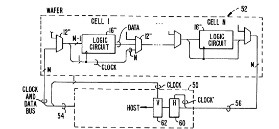
preferred clocklng scheme ls lllustrated ln Fig. 3.
As Flg. 3 lllustrates, a host computer 50 generates
data and clock signals that are communicated to a wafer 52 on
an M-blt-wlde bus 54. The wafer 52 ls formed to carry an
array of cells (cells 1, ..., N) constructed accordlng to the
present lnventlon. The clock and data slgnals are applled to
the multlplexer 12'' of the first cell of the array, cell 1,
and applled to the functlon loglc 16'' of that cell. The data
frorn the functlon logic 16'' is coupled to a multlplexer 12''
of that cell 1, and selected, along with the clock signal, for
communication through the remainlng N-l cells of the wafer 52,
and returned to the host system 50 vla the return bus 56. At
the host, the data is applled to an input reglster 60, clocked
by the clock slgnal that accompanled the data. The output of
the reglster 60 is applied to a synchronizlng reglster (or
reglsters) 62, clocked by the clock slgnal (CLOCK) that ls
applled to the wafer 52 by the lnput bus 54.
The clock slgnal, therefore, takes the same path
through the array of N cells formed on the wafer 52 as that of
17
,e~,.....
64157-322
s~ S3
the data signals. Thus, the clock is successively delayed at
each cell, thereby acqulrlng a phase shlft, relatlve to the
clock at the output of the host 50, that is equal to the delay
through the multlplexers 12''. However, when returned to the
host system 50 from the last cell, N, there is no predictable
phase delay between the origlnal, host-generated clock (CLOCK)
and that received on the return bus 56 (CLOCK). Accordingly,
the reglsters 60 and 62 are used to resynchronlze the clocks
for recelvlng data by the host system 50 in conventional
fashion.
The only potential problem ln thls scheme ls that
the clock pulse width may shrlnk or grow sllghtly at each
stage if the rise and fall times of the buffers are not
ldentlcal. A simple solutlon to the problem ls to make the
clock multiplexer/buffers inverting. Slnce there are always
four multlplexers between cells, the clock arrlves without
lnverslon, and asymmetrles in rlse and fall tlmes at one cell
are cancelled out by the next.
The net effect of the improved architecture plus the
phase-shlfted clocklng ls a galn ln performance. In prior
schemes, the minimum clock period is governed by:
( ) c ~ tr + tl + tsKEw + N tMUXMAx
where tr is the delay tlme of the (plpellne) register 18 (Flg.
1), tl is the delay of the function logic 20, tSKEW is the
clock skew, and N-t and N- tMUXMAx ls the tlme for N cells of
delay through the conflguration multlplexers 12 . In
contrast, using the cell archltecture of Fig. 1, and the
17a
64157-322
- ~ 15~3
arrangement of those cells in a llnear array as lndlcated ln
Fig. 2. the mlnimum clock perlod ls:
17b
64157-322
2~1~i853
18
c - tr tl + 4 (tMUXMAx ~ tMUXMIN)
Note-that the clock skew term has been eliminated, and
the configuration delay has been reduced to four times
the time difference between the minimum and maximum
paths through the multiplexers. On a large wafer, the
savings due-to both the skew and the multiplexer delay
terms could lead to a significant cycle time improve-
ment.
CONFIGURATION ALGORITHM:
As indicated above, a wafer scale integrated
array of cells constructed in accordance with the teach-
ings of the present invention can be configured as a
single, long chain or linear array, such as that simplis-
tically illustrated-in Fig. 2. The chain is formed
pursuant to an algorithm which initially locates those
cells sufficiently operable to be able to pass data
(and clock), and logically connects them in a chain.
Generally, the algorithm proceeds, on a cell-by-cell
basis, along the following lines: - - -
First, a cell is "opened" by asserting the
- ^ OPEN signal associated with a border of the
cell, causing the associated multiplexer to
select an IN bus (Fig. 1).
- - Second, multiplexers 12 and data paths within
the newly opened cell are tested, and if found
operable, this newly tested cell becomes the
- new terminus of the chain. If, on--the other
hand, multiplexers 12 and/or cell data paths
are found to not be operable, the border is
closed (by deasserting the associated OPEN
signal), and another cell is opened and the
test of that cell made.
The algorithm continues until the chain returns
to the cell at the periphery of the wafer serving as
the input/output of that wafer. For example, referring
to Eig. 2, assuming the wafer comprises only cells lOA,
..., 10L, and cell 10J serves as the input/output cell,
`- ~o I S~ S3
the data path chain formed by the algorithm is illustrated as
the dotted line 40. It enters the wafer at the cell 10I, and
proceeds sequentially through the cells 10I, 10E back through
10J, and continues through cells 10G, 10B, ..., 10K, returning
to the cell 10J where it is taken from the wafer of our
example.
The test performed by the algorithm may be limited,
as referred to above, to determlning whether the cell has the
data-communicating ability (i.e., workable multiplexers and
data paths) to be included ln the chaln. Once the chaln is
formed, a second testing procedure can be made to determine
the operability of the other logic clrcultry ~e.g., the
plpeline registers 18 and function logic 20). Alternatively,
the initial cell test could be to determlne the worklng
condltlon of the entire cell.
Before going lnto the conflguration algorithm in
more depth, there are additional features of the cell 10 used
in configuring the chain which need explanation. Contained in
the conflguration logic 22 ~Fig.l) are various registers and
latches that are set or reset to indicate various operating
states, modes of operation, etc. One such bank of latches is
illustrated ln Fig. 4A at 70, comprlslng lndlvidual latches
71-75. The information provided by these latches 71-75 is as
follows: The stage 75, when set, results ln assertlon of the
CHAIN signal to indlcate that the particular cell is a part of
the chaln. A cell ls not opened if thls slgnal ls asserted.
When each cell ls opened, tested, and found to be
operable, lt forms the head of the developlng chain, slgnlfied
~ 19
~ 64157-322
sgs3
by a "token" being "advanced", le.g. moved) into that newly
tested cell by setting one of the latches 71-74. The token
indicates which border of the cell brought the chaln in, and
also indicates the border to be checked for progression of the
chain into a neighbour (i.e., the ad~acent border, in a
clockwise
l9a
f~.
64157-322
2~i~3
direction, from the entry border). The signals SE, SW,
NW and NE are mutually exclusive in that only one, if
any at all, is asserted at any one time. The asserted
signal will indicate the particular corner of the cell
that is (1) bordered by the boundary crossed by the
chain for ingress to the cell and (2) the first boundary
to be checked for the next cell selected for progression
of the chain. These latches are cleared by the power-up
circuit (not shown) contained in the configuration logic
22 (Fig. 1).
One final point: Advancing the token does
not necessarily mean that the chain, as it is constructed,
will always proceed from a newly-tested cell into an
untested cell. Rather, the token could well be advanced
into an-already tested cell, such as indicated in Fig.
2 where path 40 is shown beginning at cell 10J, proceed-
ing through cell, 10I and into cell 10E. Cell 10E is,
however, bounded by the wafer periphery, and two inoper-
able cells 10A and 10F (so indicated by the Xs drawn
thereacross in phantom). The algorithm, as will be
seen, checks first to-see if the "target" cell (i.e.,
the-cell next in line for possible inclusion in the
chain) is, in fact already a part of the chain, and if
the boundary between them (the target cell and the newly
tested cell, presently holding the token) is open (when
a boundary is opened, it is opened both ways). If soj- -
the token is advanced into the target cell, even though
it is already in the chain. This is the case shown in
Fig. 2, where the path 40 returns from the cell 10E to
3C cell 10I, and from there to cell 10J. There are other
instances of this concept shown in Fig. 2.
The configuration algorithm, the main steps
of which are illustrated in Fig. 4C, proceeds along the
following lines: The wafer is powered-up (i.e, power
applied), causing the bank of latches 70 of each of the
cells 10 carried by the wafer to be reset; thereby, the
signals SE, SW, NW, NE, and CHAIN are deasserted.
~,~ j ss ~3
Referrlng to Fig. 4C, the algorithm next proceeds to the step
80, where a perlphery cell ls selected by the host computer 50
running the algorithm. The cell ("target") ls opened by
assertlon of an OPEN signal assoclated wlth the partlcular
boundary, causlng the correspondlng multlplexer 12 to select
as an lnput the IN bus assoclated wlth that boundary.
Next, ln step 81, the cell ls tested. If lt ls
found to be operable, the algorlthm advances to step 83. If,
on the other hand, the cell ls defectlve in some way, step 81
is followed by step 82, where a determlnatlon ls made as to
whether the ~ust failed cell is the last peripheral cell of
the wafer tested. If not, steps 80 and 81 are repeated untll
a workable cell is found. If no workable cell can be found at
the perlphery of the wafer, the wafer ls determlned to be bad,
and the algorlthm ends.
Assumlng that steps 80 and 81 do flnd a perlpheral
cell that ls operable, step 83 of the algorlthm ls performed:
The "token" ls advanced lnto that cell by settlng the one of
the latches 71 - 74 (Flg. 4A), corresponding to the cell's
boundary entered, and slgnlfylng that the cell ls now lncluded
ln the chain by settlng latch 75 to assert the CHAIN signal.
For example, with reference to Fig. 4B, which can be
thought of as showlng a portion 68 of a larger wafer
conslsting of four cells A, B, C, and D, each structured in
accordance wlth the teachlngs of the present lnventlon, and
orlented as dlscussed wlth respect to Flg. 2 (i.e., each cell
is rotated 180 degrees relatlve to any nelghbourlng cell).
Assume the cell D has ~ust been entered, tested, and found to
21
,.
64157-322
be in working order by the steps ~0 and 81. The token is
advanced into the cell by settlng the latch 73 to assert the
NW signal, signifying, that the chain belng formed entered the
boundary (here, W) counterclockwlse adiacent to the NW corner
of the cell D. The NW slgnal also slgnlfles the next target
cell: The cell ad~acent the boundary ls lmmedlately clockwlse
from the NW corner.
The algorithm then sets the latch 75 to identify the
cell D as now being part of the chain.
At step 84, a check ls made to determlne lf the
chaln has progressed back to the host computer 50. If so, the
algorlthm is exlted. If not, step 85 ls performed to see lf
the next cell nomlnated for lncluslon lnto the chaln ls, ln
fact, already ln the chaln (as indicated by the target cell's
asserted CHAIN slgnal). For example, referrlng agaln to Flg.
4B, as lndlcated above, the target cell of the chaln ls now
cell C. Before the OPEN slgnal lnto cell C ls asserted, there
ls a check to determine if cell C's CHAIN signal is asserted.
If so, and that border has prevlously been opened, step 85 ls
followed by step 83, and the token is advanced (setting the
appropriate one of the latches 71 - 74 of the target cell).
If not however since, the target cell ls ln the chaln, but the
boundary between them ls not open, no attempt ls made to enter
cell C. The algorithm wlll stlll return to step 83 where the
token ls advanced to the next one of the latches 71 - 75 of
the cell D to ldentlfy the next boundary corner ln order, NE.
Thus, latch 73 ls cleared and latch 74 set. The cell on the
boundary clockwlse ad~acent the NE corner of the cell, cell
22
64157-322
~o I~55
,~., is the new target cell.
r.ssume the cell C has not yet been made a part of
the chaln accordingly, the algorlthm proceeds from step 85 to
step 86 to open the target cell, cell C, by asserting the OPEN
slgnal lnto the cell. Agaln, as descrlbed above, the OPEN
slgnal causes the conflguratlon logic 22 to operate the
multiplexer 12 of cell C associated wlth the boundary between
cells D and C to select the IN bus from cell D (Flg. 1). The
algorlthm now proceeds to test cell at step 87. If the test
fails, flnding cell C to be defective ln some way, the OPEN
slgnal to cell C (generated by cell D) ls deasserted ln step
90, and a return to step 83 ls made.
If, however, cell C passes, step 87 ls left in
favour of a return to step 83, where the token ls advanced
lnto cell C by settlng the ~atch boundary ~ust crossed, l.e.,
latch 72 of that cell, to assert the SW signal, and the CHAIN
slgnal asserted by setting latch 75 of cell C. Steps 84 and
85 are performed as described above.
In this discussion, we will assume that the cells
that are clockwise ad~acent the SW and NW boundaries are
unable to pass the test performed in step 87. Thus, after the
token is first moved into cell C (step 83), steps 84, 85, 86,
87, and 90 will be performed once while latch 72 is set. The
algorlthm returns to step 83 to move the token to assert the
NW slgnal, and steps 84 - 90 again performed, again to flnd
the target inoperable. Once again the token is moved to
assert the NE slgnal, making cell B the target. Assumlng the
cell B to be good, step 87 will proceed back to step 83, and
~ 23
- t~
64157-322
B53
cell B will be included in the chain that is so far formed by
cells D, C, and B.
The algorlthm continues, until, as Fig. 2
illustrates, a return is made to a peripheral cell or the
seminal cell (cell D in Fig. 4B, or cell 10J in Fig. 2), at
which time the step 84 moves to the exit step, DONE.
Turning now to Fig. 5, there is illustrated an
exemplary use of the cell architecture 10 (Fig. 1~ ln
connection wlth a memory system forming the function logic 20.
As Fig. 5 illustrates, a cell, designated generally with the
reference numeral 110, is constructed in much the same way as
that of Fig. 1, i.e., the cell 110 is provided four edge
boundaries, north, west (N,...,W), separatlng it from its four
ad~acent neighbours. As in Fig. 1, each boundary N,...,W has
associated therewith a corresponding one of the four two-input
multiplexers 112N,...,112W, respectively. One input of each
of the multiplexers 112N, ..., 112W receives a multi-bit input
bus IN-N,...,IN-W, respectively, from the neighbour cell
located at the associated boundary. As Fig. 5 further
illustrates, each of the input busses IN-N,..., IN-W comprlses
55 signal lines, carrying 39 bits of data (DATA), 11 blts of
address (ADDR), four bits of instruction (INSTR), and a
periodic clock (CLOCK) signal. Three of the multiplexers,
112N, 112E and 112W, couple thelr respectlve 55-blt outputs to
a second input of the multiplexer associated with a clockwise
ad~acent boundary. The remaining multiplexer, 112S, has its
55-bit output coupled to logic circuit 116, where lt is
received by the lnput of a plpeline register configuratlon 118
- 24
~ ~,
"
64157-322
- ;~o / 5~ 53 .
that is clocked by the CLOCK signal. The loglc circult 116
(whlch corresponds to the loglc clrcult, 16 ln Flg. 1)
lncludes, ln addltion to the plpellne reglster conflguratlon
118, a dynamlc random access memory conflguratlon 140 of
conventlonal design, a decode circuit 142 that ls coupled to
control logic, 144. Address reglsters 146 are also lncluded,
as ls a shift/pass multiplexer 148.
The signalling produced by the control logic 144
directs operation of the cell in response to various
instructions decoded by the decode loglc 142. Thus, for
example, the selected one of the latches 22 (e.g., 22W, Fig.
6) ls set by signalllng from the control loglc and
communlcated to the configuration latches 122 which, in turn,
causes another of the selection signals SEL-N,...,SEL-E to be
asserted (in addition to the one asserted by the OPEN signal
from the neighbour cell that caused this cell to be entered).
One particularly advantageous implementatlon of
wafer scale lntegratlon is the promise it holds for solid
state memory systems. Using a chain-conflguratlon, formed as
hereln above descrlbed, constructed of many slmllarly-
structured cells 110, carrylng mernory as lllustrated ln Flg 5,
a very hlgh capaclty memory archltecture can be obtalned. The
DRAM 140 could very well be structured as an N by 39 blt word
memory. However, 39 blt words are unusual. Therefor, lt ls
more llkely that the DRAM 140 conflguration ls N by M (N
words, each M bits ln length). If, however, the word length
deslred to be used is larger, for example, than M blts, the
shlft/pass multiplexer 148 can be used. For example, using
24a
64157-322
~ ~sg~3
the cell architecture of the present invention, together with
a cell memory structure as shown in Fig. 5, a number of such
cells 110
24b
64157-322
2~ 3
forming a wafer scale integrated circuit memory have
the potential of providing immense storage capacity.
If DRAM 140 is an N by 1 bit RAM, this configuration
is best believed implemented by having each addressable
(multi-bit) word spread across a number of cells 110.
For this reason, the the shift/pass multiplexer 148 is
used: In memory write operations, the shift/pass multi-
plexer 148 functions to strip the least significant bit
(LSB) of the DATA word presented to that cell 110 for
storage in the memory configuration 140. The shift/pass
multiplexer 148 then shifts the remainder of the word
down (moving the least next least significant bit (LSB
+ 1) into the LSB position) before it is communicated
to the next cell in the chain, where the same operation
occurs.
The shift/pass multiplexer 148 functions in
reverse when involved in a read operation: Access to
the memory configuration 140 produces a single bit that
is added to a word as it (the word ) passes through
the particular cell 110.
Operation of the cell 110, and the memory
function is carries, generally is as follows: Paral-
lel, multi-bit information, containing the 39 bits of
data (DATA), 11 bits of address (ADDR) and 4 bits of
instruction (INSTR), all accompanied by the periodic
clock (CLOCK) signal, are applied to a chain formed by
a number of cells 110, and sequentially applied to each
cell in order. When applied to the cell 110, the infor-
mation enters the pipeline register 118, and from there
coupled to the memory system of function logic 120.
The instructions, INSTR (e.g., read, write, etc.), are
communicated to the decode register 142 where they are
decoded for application to the control logic 144. At
the same time, an address, ADDR, indicating the memory
location to be accessed for a read or write operation
is applied to the address register 146. Control logic
144 then operates to perform the access of the DRAM
20~5853
26
140. In the case of a write, data appearing at the
data input (DI) of the DRAM 140 is write to-the specified
memory location; and in the case of a read, the accessed
data is coupled from the data output ~D0) of the DRAM
140 to the output bus of the cell 110, OUT-W, via the
signal lines 134.- Depending upon how the cell 110 was
configured by the configuration algorithm hereinabove
described, the output of the logic circuit 116 will be
communicated directly to the OUT-W output bus, as well
as being conducted to the output busses OUT-W, N, E by
the multiplexers 112W, 112N, or 112E, respectively.
The cell next in order in the chain will be configured
to have one of its multiplexers 112 set to select the
connection to the output bus of this cell 110.
The address register structure 146 is used
for configuring the address base of the DRAM 140 of the
cell 110, relative to DRAMs that may be contained in
other cells-of a-wafer-scale integrated array of cells
llO as described hereinabove. Address reyisters 146
may be set to specify the address boundaries of the
address space implemented by the DRAM-140. -Addresses
for a read or write operation that are within this
address space will cause the address register 146 to
enable the control logic 144 to cause access of the-
DRAM 140. Conversely, addresses that are-not within
the-address space specified ~y the address regis-ters
146 will not be able to access the DRAM 140 of the par-
ticular cell 110. (Although another of the cells 110
in the hypothetical array will have this address within
its address space specified by the address registers
146.)
In summary, there has been presented a descrip-
tion of an architecture of a cell for ~se in a wafer-scale
integrated array of identically structured cells. That
architecture contemplates selection apparatus formed on
each cell, in connection with other logic circuitry, in
such a way that the logic circuits of the various cells
20~5853
27
of the array can be logically interconnected by the
connection apparatus to form a linear array or chain of
such cells. When so formed, there is a known, and min-
imum, delay formed between each logic circuit and the
next one in the chain.
While a detailed explanation of the present
invention has been presented, it should be evident to
those skilled in the art that various modifications can
be made. For example, the configuration latches 71-75
can be replaced with fuses that perform the sample func-
tion, with the cells being tested by probed connections
from the host, and the fused connections interrupted as
a result of the test to configure each cell in the chain.
Further, while the foregoing discussion has referred to
an array of identically constructed cells, this need
not be true to practice the present invention. For
example, certain of the cells 10 may carry memory as
the logic function 20, while others may carry arithmetic
logic units, or other digital function. Also, the config-
uration may be made the subject of a number of modifica-
tions and variations. When a cell is entered during
formation of the chain, all boundaries of that cell
could be opened, and the first of the open boundaries
found to separate that cell from another target cell
becomes the one across which the token is advanced.
Finally, the discussion presented herein
describes use of the invention for forming a linear
array of cells from a wafer scale integrated array of
such cells. While this is the best mode known of using
the invention, it is by way of illustration only. As
pointed out at the outset of this discussion, the inven-
tion is applicable to any array, and need not be neces-
sarily confined to use in wafer scale integration.