Note: Descriptions are shown in the official language in which they were submitted.
-1- 2~
HIGH DENSITY RIBBON CABLE CONNECTOR
This invention relates to electrical connectors
and, in particular, to a high density ribbon cable
connector wherein a predetermined minimum spacing is
maintained between all features of any contact and other
nearby contacts.
Ribbon cable connectors for mass terminating to
ribbon cable at a location remote from an end of the
cable, such as in a daisy chain configuration, are
disclosed in U.S. Patents 3,820,055; 4,068,gl2;
4,475,786; and 4,693,533. As the downsizing of
electronic devices has progressed, more contacts are
placed in smaller and smaller connectors to consume less
space on a printed circuit board. The complementary
connectors, typically a cable connector, must also
contain a higher density of contacts. As the density of
contacts in ribbon cable connectors increases, the
spacing between adjacent conductors in ribbon cable
adapted to be terminated to the ribbon cable connector
decreases correspondingly. Typically, the
interconductor spacing is reduced to one-half of the
spacing of the previous generation cable. As the
spacing between ribbon cable connectors decreases,
positioning contacts in a connector housing at an
appropriate spacing, separated by dielectric material
while positioning insulation displacements plates in an
array appropriate for mass termination to the ribbon
14475 CA
*
2~8~
' -2-
-
cable has become more critical. Small variations in the
positioning of contacts in the housing or movement of
contacts during termination of the ribbon cable can
cause shorting between adjacent conductors. Due to the
closeness of spacing of the contacts, greater attention
must be paid than in the past to the sufficiency of
dielectric material or air space separating the closest
portions of adjacent contacts to assure that the
contacts can withstand voltage levels sufficient to make
the connector of practical use.
There is disclosed in U.S. Patent 4,753,608 an
electrical connector for terminating at least two layers
of conductors. The electrical connector includes a
housing having a higher top surface and a lower top
surface; a plurality of longer contacts with their
piercing portions projecting from the higher top
surface; a plurality of shorter contacts with their
piercing portions projecting from the lower top surface;
a first retainer member adapted to be mounted on the
higher top surface; a second retainer member adapted to
be mounted on the lower top surface; a device for
temporarily mounting the first and second retainer
members so that the first and second layers of
conductors are held adjacent to the piercing portions of
the longer and shorter contacts; and a device for
latching the first and second retainer members to the
insulating housing so that the first and second layers
14475 CA
2~L58~3
-3
of conductors are connected to the longer and shorter
contacts, respectively, when the first and second
retainer members are further pushed toward the
insulating housing.
In accordance with the present invention, a high
density electrical connector for terminating to
conductors of a ribbon cable has an insulative housing
defining a cable receiving face, a mating face and at
least one row of contact receiving passages extending
therebetween with contacts secured therein. The
contact receiving passages open into opposing channels
near the cable receiving face. At least first and
second contacts include a mating portion, an
intermediate section and an insulation displacement
plate. The intermediate section is defined by a pair of
sheared edges extending toward the insulation
displacement plate from the mating section. The mating
portion and a first section of the intermediate portion
are substantially planar. The conductor terminating
portion and a second section of the intermediate portion
are also substantially planar and formed to be
substantially perpendicular to the mating portion and
the first section of the intermediate portion. The
intermediate portion defines an insertion shoulder
facing the conductor terminating portion. The first
contact has a respective insertion shoulder positioned a
first predetermined distance from a respective conductor
14475 CA
` 2~ 8
-4-
terminating portion. A second contact has a respective
insertion shoulder positioned a second predetermined
distance from a respective conductor terminating
portion, where the second distance is less than the
first distance. The first and second contacts are
received in adjacent passages in a row of passages,
whereby the first contact can be inserted into a passage
by applying a force to the insertion shoulder thereof
and subsequently a second contact can be inserted into a
passage by a tool applying a force to the insertion
shoulder thereof without the tool interfering with the
insertion shoulder of the first contact.
An embodiment of the invention will now be
described by way of example with reference to the
accompanying drawings, in which:
FIGURE 1 is an offset cross-sectional view of a
ribbon cable connector in accordance with the present
invention mounted to a panel and terminated to a ribbon
cable;
FIGURE 2 is a plan view of two adjacent inside
contacts as stamped on a carrier strip;
FIGURE 3 is a plan view of the two adjacent inside
contacts of Figure 2 with the receptacle of each formed
perpendicular to the plane of the insulation
displacement plate;
FIGURE 4 is a perspective view of an inside
contact;
14475 CA
2015~S98
-
FIGURE 5 is a plan view of two adjacent outside
contacts as stamped on a carrier strip;
FIGURE 6 is a plan view of the two adjacent outside
contacts of Figure 5 with the receptacle portion of each
formed perpendicular to the plane of the insulation
displacement plate;
FIGURE 7 is a perspective view of an outside
contact;
FIGURE 8 is a perspective view, partially in
section, of the ribbon cable connector;
FIGURE 9 is a perspective view of the ribbon cable
connector; and
FIGURE 10 is a partial sectional view showing the
insulation displacement plates of a row of contacts
received in the housing.
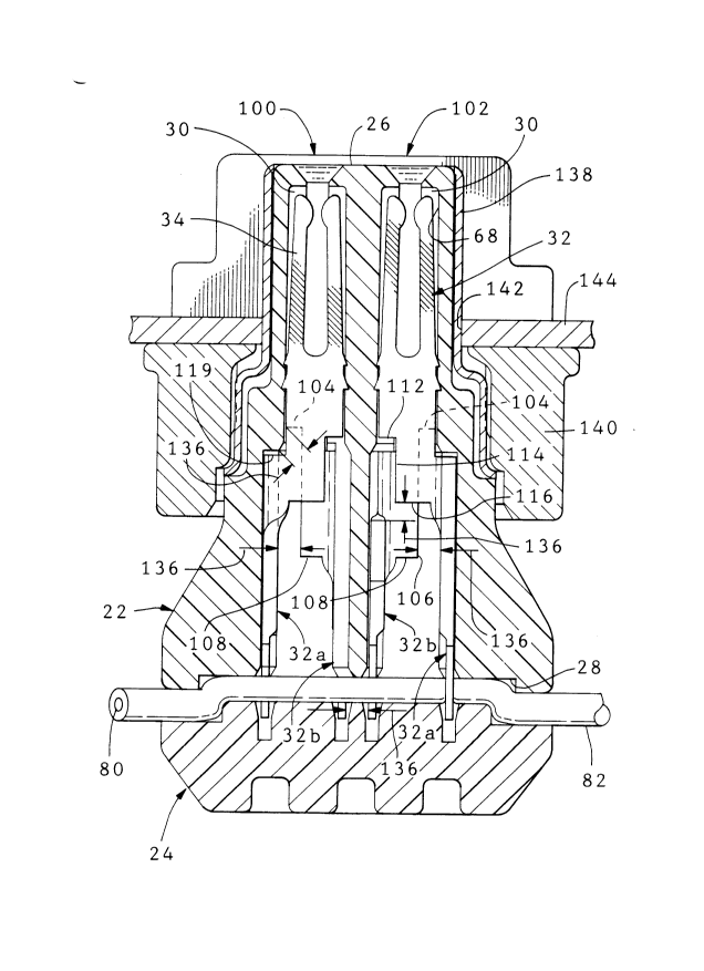
A high density ribbon cable connector 20, in
accordance with the present invention, is shown in a
cross-sectional view in Figure l. Although connector 20
is shown as a shielded connector, connector 20 could be
unshielded, as shown in Figure 8. Connector 20 includes
housing 22 and termination cover 24, both molded of a
dielectric material. In a preferred embodiment, housing
22 and termination cover 24 are molded of a plastic
material having substantially no shrink rate such as a
liquid crystal polymer sold under the trade name
"Vectra-130."
14475 CA
2~o~s89~
_ -6-
Housing 22 has a forward mating face 26, opposed
conductor receiving face 28 and contact receiving
passages 30 extending therebetween, with contacts 32
secured therein. In the preferred embodiment, contacts
32 are positioned in housing 22 with the mating portion
34 in the form of receptacle 36 in two rows spaced with
centerline 0.100 (2.5mm) apart; adjacent receptacles in
each row are spaced with centerlines 0.050 inch (1.27
mm) apart, and connector 20 is designed to terminate a
ribbon cable having 0.025 inch (0.635 mm) centerline
spacing between conductors.
Contacts 32, as best seen in Figures 2-7, are
stamped and formed from rolled strip stock, typically
phosphorous bronze. A portion of the width of the
rolled stock is premilled to provide a thinner region
along an edge of the strip stock. Each contact 32 has a
mating portion 34 at one end, an insulation displacement
plate 38 at the other end, and a intermediate portion 40
therebetween. Mating portion 34 of each contact is
stamped in the thicker portion of the stock. The
insulation displacement plate 38 is stamped in the
thinner region of the stock. As best seen in Figures 2,
3, 5 and 6, contacts 32 are stamped on the same
centerline spacing as they will be received in housing
22. Figures 2, 3, 5 and 6 show contacts 32 stamped and
formed with their relative positions maintained by a
carrier strip 42. The spacing 44 between the insulation
14475 CA
2(~:3L5898
-7-
displacement slots 46 (Figure 2) of adjacent contacts 32
is 0.100 inch (2.5 mm) as is the centerline spacing of
the formed receptacle 36 (Figure 3). Mating portion 34
in the form of receptacle 36 is comprised of a pair of
opposed cantilever beams 48,50 extending forwardly from
intermediate portion 40 to free ends 52,54 and define
therebetween tab receiving slot 56. Free ends 52,54 are
tapered inwardly toward tab receiving slot 56 at taper
58 to assist in guiding a tab of a complementary
connector (not shown) in to slot 56. Curved surfaces 60
provide a surface for a tab to engage. In a preferred
embodiment, receptacle 36 is substantially symmetrical
about centerline 62.
Outer sheared surfaces 64,66 of beams 48,50 taper
gradually away from the centerline 62 in a direction
from free ends 52,54 toward intermediate portion 40. As
best seen in Figure 1, should surfaces 64 or 66 engage a
wall 68 of contact receiving passage 30, the wall
functions as an anti-overstress feature. The outer
sheared edge surfaces 70,72 through regions 74 of
intermediate portions 40 are also symmetrical about
centerline 62 and may be parallel. Barbs 76 on
intermediate portion 40 extend beyond side edges 70,72.
Upon insertion of contact 32 into passages 30, barbs 76
plow through passage walls 68 with plastic flowing
around the barbs to provide an interference fit that
secures contact 32 in passage 30.
14475 CA
2Q~
_ -8-
Insulation displacement plate 38 is fabricated in
the thinner, premilled portion of the stock, with taper
78 defining the transition between the thicker and
thinner portions of the stock. Insulation displacement
plate 38 is thinner to facilitate insulation
displacement termination of conductors 80 of ribbon
cable 82 by reducing the force necessary to effect a
termination. Insulation displacement plate 38 has a
widened base region 84, the sides of which are defined
by precisely spaced shear edges 86,88. A pair of spaced
insulation piercing tines 90,92 extend rearwardly from
base region 84 to insulation piercing points 94 at the
distal ends and define conductor receiving slot 46
therebetween. Tapered lead-in surfaces 96 angle toward
conductor receiving slot 46. Slot 46 extends into
widened base region 84 of plate 38, with the base region
84 beginning about half way along slot 46. As best seen
in Figures 3 and 6, slot 46 is substantially parallel to
centerline 62 and laterally displaced therefrom at
lateral spacing 63. Contacts 32 are severed from
carrier strip 42 as indicated by broken line 98.
As best seen by comparing Figures 2, 3 and 4 to
Figures 5, 6 and 7, respectively, there are two types of
contacts 32 with the general features described above.
The two contacts are designated either outside or
inside. Contact 32a will be referred to as an outside
contact because the insulation displacement plates 38 of
14475 CA
2~1~.8~8
- - 9 -
contacts 32a form the two outer rows of insulation
displacement plates, as best seen in Figures 1, 8 and 9.
Contacts 32a are also shown in Figures 5, 6 and 7.
Contacts 32b will be referred to as inside contacts
because insulation displacement plates 38 of contacts
32b form the two inner rows of insulation displacement
plates, as best seen in Figures 1, 8 and 9. Contacts
32b are also shown in Figures 2, 3 and 4.
The mating portion 34 of outer row of contacts 32a
and the mating portion of adjacent inner row of contacts
32b alternately interdigitate to form a first row 100 of
receptacles 36. Similarly, the mating portion of the
other outer row of contacts 32a and the mating portion
of the adjacent inner row of contacts 32b alternately
interdigitate to form a second row 102 of receptacles.
With reference to Figures 2, 3 and 4, inside
contact 32b is shown. In Figure 2, adjacent contacts
32b are shown stamped on centerline, integral with
carrier strip 42. The entire contact, prior to forming,
is substantially in the plane of the original stock.
Sheared surface 72 has been notched out of intermediate
portion 40 forming shoulder 104 and sheared surface 106.
The location of shoulder 104 and the depth of the notch
forming sheared surface 106 are both predetermined as
discussed below. Shoulder 108 extends on both sides of
centerline 62 and provides a rearward facing insertion
shoulder on which an insertion force can be applied, on
14475 CA
.` 2Q~5898
--10--
both sides of centerline 62 to overcome the resistance
to insertion provided by barbs 76 engaging wall 68, to
insert contact 32b into passage 30 during manufacture of
connector 20. Since the insertion force can be applied
to shoulder 108 on both sides of centerline 62, there is
no moment to rotate the receptacle. Lateral offset
section 110 is within intermediate portion 40 of contact
32b. A first portion 39 of lateral offset section 110
is rearward of mating portion 34, defines shoulder 108
and forward edge 111. A second portion 41 of lateral
offset section 110 is contiguous with first portion 39
and interconnects with insulation displacement plate 38.
Contact 32b is formed through lateral offset section 110
such that mating portion 34 is in a plane substantially
perpendicular to the plane of insulation displacement
plate 38. First portion 39 substantially remains in the
plane of mating portion 34; second portion 41
substantially remains in the plane of insulation
displacement plate 38.
Figure 3 shows inside contacts 32b with receptacle
36 and first portion 39 formed to be perpendicular to
insulation displacing plate 38 and second portion 41.
In this formed position of the preferred embodiment, the
centerline of receptacle 36 is laterally offset from the
centerline of slot 46 at lateral offset 63 by half of
the centerline spacing of the conductors 80 of cable 82
adapted to be terminated to connector 20.
14475 CA
2~58~8
--11--
-
In Figure 5, adjacent contacts 32a are shown
stamped on centerline, integral with carrier strip 42.
The enti~e contact, prior to forming, is substantially
in the plane of original stock. Sheared surface 72 of
contacts 32a has been notched out of intermediate
portion 40 forming shoulder 112 and sheared surface 114.
The location of shoulder 112 and the depth of the notch
forming sheared surface 114 are both predetermined, as
discussed below.
Shoulder 116 extends on both sides of centerline 62
and provides a rearward facing insertion shoulder on
which an insertion force can be applied. The insertion
force is applied on both sides of centerline 62 to
overcome the resistance to insertion provided by barbs
76 engaging wall 68, to insert contact 32a into passage
30 during manufacture of connector 20. Since the
insertion force can be applied to shoulder 116 on both
sides of centerline 62, there is no moment to rotate the
receptacle. Shoulders 108 and 116 are displaced along
centerline 62 of contacts 32b and 32a such that one of
the insertion shoulders is more forward than the other.
In the preferred embodiment, shoulder 116 is more
forward on contact 32a than shoulder 108 is on contact
32b. Thus, outside contacts 32a may be mass inserted
with a tool pushing on shoulder 116; subsequently,
inside contacts 32b may be mass inserted with a tool
pushing on shoulder 108. In this sequence, the tool
14475 CA
2~589~3
_ -12-
used to insert contacts 32b does not interfere with
shoulder 116.
Lateral offset section 118 is within intermediate
portion 40 of contact 32a. A first portion 121 of
S lateral offset section 118 is rearward of mating portion
34, defines shoulder 116 and forward edge 119. A second
portion 123 of lateral offset 118 is contiguous with
first portion 121 and extends rearward through carrier
strip 42 to interconnect with insulation displacement
plate 38. Contact 32a is formed through lateral offset
section 118 such that mating portion 34 is in a plane
substantially perpendicular to the plane of insulation
displacement plate 38. First portion 121 substantially
remains in the plane of mating portion 34; second
portion 123 substantially remains in the plane of
insulation displacement plate 38. Lateral offset
section 118 has a shear edge 120 that is within the
profile of mating portion 34 of the adjacent contact in
that sheared edge 120 falls within the notch formed by
shoulder 112 and sheared surface 114.
Figure 6 shows outside contacts 32a with receptacle
36 and part of intermediate portion 40 forward of
shoulder 116 formed to be perpendicular to insulation
displacing plates 38 and second portion 123. In this
formed position of the preferred embodiment, the
centerline of receptacle 36 is laterally offset from the
centerline of slot 46 at 122 by half of the centerline
14475 CA
2~8g~
-13-
spacing of the conductors 80 of cable 82 adapted to be
terminated to connector 20. In this manner, as shown
best in Figure 9, the slots for receiving conductors 80
are staggered in connector 20 such that each conductor
terminates to a predetermined contact, as is known in
the art.
As best seen in the partial sectional view of
Figure 8, the receptacle portion of outside contacts 32a
are received in every other receptacle receiving passage
124, of passages 30, in a row of receptacles 100 or 102.
The receptacle portion of inside contacts 32b are
received in the remaining receptacle receiving passages
126, of passages 30, in a row of receptacles 100 or 102.
As best seen in Figure 10, base region 84 of
insulation displacement plate 38 is received in a
channel 128 defined by ribs 130. Sidewalls 132,134 of
ribs 130 define therebetween a space substantially the
same as the distance between shear edges 86,88 of base
region 84. Thus, when contact 32 is received in passage
30, with base region 84 received between ribs 130, shear
edges 86,88 are positioned against sidewalls 132,134 so
as to precisely position insulation displacement plate
38, tines 92 and slot 46 in connector 20, as well as to
prevent plate 38, tines 92 and slot 46 from moving
laterally during termination of cable 82.
The spacing between the tines of back-to-back
contacts in the two rows of inside contacts, as seen in
14475 CA
898
-14-
Figures 1 and 9 and as indicated in Figure 1, is the
minimum distance 136 between any two points of any
features of any two contacts in connector 20. All
features of contacts are separated by at least this
minimum distance. With reference to Figure 1, the depth
of notches generating sheared surfaces 106 and 114 are
selected to maintain at least the minimum spacing 136
between-the respective sheared surfaces and the closest
feature on a contact received in an opposing channel
128. The location of shoulder 116 is selected relative
to the forward edge 111 to be at least the minimum
spacing 136. The location of shoulder 104 is selected
relative to the forward edge 119 to be at least the
minimum spacing 136. In the above manner, a high
density connector is provided that maintains at least a
minimum distance through air between all features on any
one contact and any features on other nearby contacts to
minimize the potential of arcing between contacts such
that signal voltages carried on the contacts can reach a
voltage level that is practical for using the connector.
In the preferred embodiment, this minimum air spacing is
about 0.025 inch (0.635 mm).
Housing 22 has a terminating cover 24 securable
thereto for effecting mass termination for ribbon cable
82 or maintaining ribbon cable 82 in the terminated
position. Any known terminating cover will suffice.
One such terminating cover is disclosed in copending
14475 CA
2(~89~3
-
application serial number 07/304,046 filed January 30,
1989 entitled "Strain Relief for Ribbon Cable
Connector," the disclosure of which is hereby
incorporated by reference.
Connector 20 is shown in Figure 1 as a shielded,
panel mount connector. The mating end of connector 20
is surrounded by a drawn shell 138 which is electrically
commoned with a die cast housing 140 in accordance with
the teaching of U.S. Patent 4,808,125, the disclosure of
which is hereby incorporated by reference. Drawn shell
138 extends through an aperture 142 in panel 144 and is
secured thereto.
14475 CA