Note: Descriptions are shown in the official language in which they were submitted.
-1- 201 6302
FIBER OPTIC GYRO WITh' PULSATING LIGHT SO~CE
AND CORRESPONDING SPIKE FILTERING
BACKGROUND OF T~E INVENTION
The present invention rel2tes to a fiber optic
gyro which employs a semiconductor laser or super
luminescent diode as a light source and, more
particularly, to a fiber optic gyro designed for less
power consumption and wider application range of
temperature.
Fig. 1 shows a conventional fiber optic gyro.
Light emitted from a light source 11 is applied via an
optical coupler 12 and a polarizer 13 to an optical
coupler 14, from which it is input, as rlaht-handed light
and left-handed lignt, into an optical fiber coil 15 at
both ends thereof. The right-handed and the left-handed
light having propacated through the optical fiber coil 15
in opposite directions are coupled together by the
optical coupler 1~ and interfere with each other. The
resulting interference light is provided via the
polarizer 13 and the optical coupler 12 to a
photodetector 16, wherein it is converted into an
electrical signal.
When no angular velocity is being applied to the
optical fiber coil 15 in the peripheral direction
thereof, the phase difference between the right-handed
and the left-handed light in the optical fiber coil 15 is
substantially zero. When an angular velocity Q is
applied to the optical fiber coil 15 in its peripheral
direction, a so-called Sagnac eEfect is produced, by
which a phase difference is introauced between the right-
handed and the left-handed light in the optical fiber
coil 15. As is well-known in the art, the phase
difference ~Q is expressed by
-2- 20163~2
4nRL Q ... (1)
where R is the radius of the optical fiber coil 15, L is
the length of the optical fiber coil 15, A is the
wavelength of light in a vacuum, C is the velocity of
light, and Q is the input angular velocity.
The intensity Io of the interference light
having reached the photodetector 16 is as follows:
Io = 2 (l + COS~Q ) . . . ( 2)
where Imax is a maximum quantity of light.
Therefore, the angular velocity Q can be
detected by measuring the intensity Io of the
interference light. In this instance, however, when the5 input angular velocity Q is small, the phase difference
is small and therefore a change in cos~n is small,
so that the input sensitivity becomes extremely low.
To avoid this and hence optimize the input
sensitivity, it is customary in the prior art to
interpose between one end of the optical fiber coil 15
and the optical coupler 14 a phase modulator 17 in which
the right-handed and the left-handed light are phase
modulated by a drive signal available from a phase
modulator drive circuit 18 as shown in Fig. l. Fig. 2
shows the relationship between the phase modulating
signal SM and the interference light when the signal SM
is a sine wave, and Fig. 3 shows the abovesaid
relationship when the signal SM is a rectangular wave.
In either case, the intensity Io Of the
interference light resulting from the phase modulation
contains the following component:
Is = Ks-sin~-cos(~t + ~) ... (3)
where Ks is a constant, ~ is the angular velocity of
3 2~1~3~2
.
phase modulation, and ~ is the phase difference between
the phase modulating signal SM and the Ks sin~
component.
Synchronously detecting the output signal of the
photodetector 16 by a synchronous detector 19 with a
signal which is synchronized with the phase modulating
signal SM~ the synchronous detector 19 yields the
following output V:
V = K-sin~ ...
where K is a constant.
The phase ~ in Eq. (4) is the phase difference
between the right-handed and the left-handed light in the
optical fiber coil 15, which is expressed as follows:
Q + l~f ( 5)
where the phase difference ~f represents the phase
difference introduced between the right-handed and the
left-handed light by a feedback phase modulator 21
interposed between the other end of the optical fiber
coil 15 and the optical coupler 14 as depicted in Fig. 1.
The phase difference ~f can be created by phase shifting
the right-handed and the left-handed light at a fixed
rate by the feedback phase modulator 21. In practice,
the phase shift is effected by applying a ramp voltage
from a ramp voltage generator 22 to the feedback phase
modulator 21.
When applying the ramp voltage to the feedback
phase modulator 21, the right-handed light (hereinafter
referred to as CW light) undergoes such a phase shift as
indicated by the solid line at row A in Fig. 4, whereas
the left-handed light (hereinafter referred to as CCW
light) is delayed behind the CW light for a period of
time I for the propagation of the CCW light through the
optical fiber coil 15 and is then similarly phase shifted
~ ~4~ 2016~02
as indicated by the broken line. As a result of this,
the phase difference ~f between the CW light and the CCW
light becomes such as shown at row B in Fig. 4. In this
case, if the ramp voltage is applied so that a maximum
value of the phase shift ~R of each light is 2nk (where k
is an integer), the phase difference a~f between the CW
light and the CCW light is expressed as follows:
2nnL
~f = C k-f ..- (6)
where f is the frequency of the ramp voltage. The output
of the synchronous detector 19 is applied to an
integrating filter 23, the output of which is provided to
the ramp voltage generator 22, thereby generating
positive and negative ramp voltages of a frequency
corresponding to that of positive and negative input
voltages. By controlling the frequency of the ramp
voltage so that the Sagnac phase difference ~Q between
the CW light and the CCW light in the optical fiber coil
15 is cancelled by the phase difference ~fr a closed
loop is established and the frequency f of the ramp
voltage is obtained from Eqs. (1), (S) and (6) as
follows:
f nAk Q -- (7)
By measuring the frequency f of the ramp voltage based on
Eq. (7), the input angular velocity Q can be obtained
with nAk as a proportional constant. Incidentally,
since it is easy for those skilled in the art to measure
the frequency f of the ramp voltage, no particular means
therefor is shown in Fig. 1.
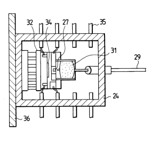
The light source 11 may have such a structure as
shown in Figs. SA and 5B which are horizontal and
~5~ 2~163~2
vertical sectional views. In a case 24 closed by a lid
25 a heat sink 26 for a light source element 27 is
disposed, on which the light source element 27 is
mounted, and a spherical end optical fiber 29 having a
spherical tip is fixed by solder 31 on an optical fiber
support 28. The light source element 27 and the
spherical end optical fiber 29 are appropriately aligned
so that light from the former is incident to the latter.
On the heat sink 26 there are mounted a Peltier device 32
for cooling it and a thermistor 33 for sensing its
temperature. Further, a photodetector 34 for monitoring
the quantity of light is provided which receives light
from the light source element 27. The light source
element 27, the thermistor 33 and the photodetector 34
are connected to hermetic terminals 35 mounted on the
case 24, which is, in turn, mounted on a mounting plate
36.
As depicted in Fig. 6, the output of the
photodetector 34 is applied to an automatic light control
circuit 37, by which the quantity of light emanating from
the light source element 27 is controlled constant. The
thermistor 33 is connected to a bridge circuit 39 in a
temperature control circuit 38. The bridge circuit 39
yields an error signal between the temperature of the
heat sink 26 detected by the thermistor 33 and a
predetermined temperature. The error signal is amplified
by an error signal amplifier 41 and is then provided to a
Peltier device drive current generator 42, by which the
drive current for the Peltier device 32 is controlled so
that the temperature of the heat sink 26 becomes equal to
the predetermined value.
As the light source element 27 for use in the
light source 11, a super luminescent diode (hereinafter
- -6- 2~163~2
referred to simply as SLD), which emits light of a large
spectral width, is often employed for the purpose of
lessening the influence of noise arising from the
backward Rayleigh scattering, coupling of light between
different polarization modes and the Kerr effect in the
optical fiber coil 15, that is, for the purpose of
providing a highly accurate fiber optic gyro. However,
the drive current of the SLD greatly varies with the
temperature of the heat sink 26. Fig. 7 shows the
relationship of the SLD drive current to the temperature
of the heat sink 26 in an SLD module.
Now, assuming that the quantity of light emitted
from the spherical end optical fiber 29 of the SLD module
is set to one-half of a maximum quantity of light 1 mW
available from the SLD, that is, 500 ~W, the temperature
- applicable to the SLD heat sink 26 is around 45C at the
highest; namely, the SLD module cannot be used in, for
example, a +85C atmosphere needed in MIL or the like.
In general, the temperature of the SLD heat sink
26 is controlled to remain constant, for instance, at
40C by using the Peltier device 32. The Peltier device
32 used in the light source module shown in Figs. 5A and
5B has such characteristics as shown in Fig. 8.
In Fig. 8, Q indicates the quantity of heat
discharged on the cooling side of the Peltier device 32,
which can be made to correspond to the quantity of heat
generated by the light source element 27 mounted on the
cooling surface. Strictly speaking, the amount of heat
discharged on the cooling surface of the light source
element 27 includes heat traveling from the spherical end
optical fiber 29 and heat by radiation and convection in
the light source module as well as heat generated by the
light source element 27. Hence it must be taken into
_ -7- 2 a 1 6 3 ~ 2
account that the actual performance of the Peltier device
23 is lower than its performance depicted in Fig. 8,
obtained by testing the Peltier device singly. As seen
from Fig. 8, when the Peltier device drive current
exceeds 1 A, the heat absorption efficiency decreases.
Therefore, the Peltier device drive current may
preferably be 1 A or more.
Assuming that the output light of the spherical
end optical fiber 29 is 500 ~uW as mentioned previously,
the surrounding temperature at which the Peltier device
drive current exceeds 1 A is about 81C, below the
required temperature +85C, as seen from data during
continuous drive of the SLD shown in Fig. 9.
On the other hand, power that is consumed for
temperature control of the SLD module is expressed as the
sum of power consumed by the temperature control circuit
38 and power by the Peltier device 32. Since the power
required for the bridge circuit 39 and the error signal
amplifier is smaller than maximum power for the Peltier
device drive current generator 42 and the Peltier device
32, the overall consumed power is determined essentially
by the power that is consumed by the Peltier device drive
current generator 42 and the Peltier device 32. Now,
assuming that the power source voltage of the Peltier
device drive curzent generator 42 is a voltage 5 V which
permits the Peltier device 42 to stably effect
temperature control and is considered to be relatively
easily available from the system employing the fiber
optic gyro and that a maximum current flowing through the
Peltier device 42 is limited to 1 A, maximum power
consumed by the temperature control is 5 W. This value,
considered in combination with consumed power of other
electric circuits, is equal to or greater than consumed
_ -8- 2016302
power of a conventional gyroscope which utilizes the
Coriolis effect.
As described above, the conventional iber optic
gyro employs the SLD element for higher measuring
accuracy and controls the temperature of the SLD element
by the Peltier device for enlarging the working
temperature range. Moreover, its light source module
usually employs a small Peltier device for the purposes
of minimizing its power consumption for temperature
control and miniaturizing the light source module.
Therefore, the conventional fiber optic gyro is
inoperable at the highest temperature in its working
temperature range, and in spite of using the small
Peltier device, power consumption is maximum power
consumed as much as 5 W for temperature control alone,
which is equal to or greater than the power consumption
of the gyroscope utilizing the Coriolis effect.
SUMMARY OF THE INVENTION
It is therefore an object of the present
invention to provide a fiber optic gyro which has its
working temperature range above 85C and consumes less
power.
To attain the above objective, the fiber optic
gyro of the present invention includes means for
intermittently driving the light source. The provision
of such means permits the working temperature means of
the fiber optic gyro up to +85C or more and affords
reduction of its power consumption while achieving
required functions and performance of the gyro. To
maintain high accuracy of the fiber optic gyro, bias
eliminating means is disposed at the preceding stage of
the synchronous detector to eliminate an intermittent
- - 9 - '~ 0 1 6 3 02
frequency component, and in the case of further
increasing accuracy, a gate circuit is provided at the
succeeding stage of the synchronous detector, by which
both end portions of the synchronous detector output are
cut off to remove spike noises.
BRIEF DESCRIPTION OF THE DRAWINGS
Fig. 1 is a block diagram showing a conventional
fiber optic gyro;
Fig. 2 is a diagram for explaining phase
modulation by a sine wave and the resulting interference
light;
Fig. 3 is a diagram for explaining phase
modulation by a rectangular wave and the resulting
interference light;
Fig. 4 is a diagram showing feedback signals of
the fiber optic gyro depicted in Fig. l;
Fig. 5A is a plan view of a light source module,
with its case cut off horizontally;
Fig. 5B is a side view of the light source
module, with its case cut off vertically;
Fig. 6 is a block diagram showing temperature
control and automatic light control structures of the
light source module;
Fig. 7 is a graph showing the relationship
between the heat sink temperature of an SLD and its drive
current;
Fig. 8 is a graph showing characteristics of a
Peltier device;
Fig. 9 is a graph showing the relationship of a
Peltier device drive current to the surrounding
temperature of the SLD module;
Fig. 10 is a block diagram illustrating an
-lO- 20163~2
embodiment of the fiber optic gyro of the present
invention;
Fig. 11 is a waveform diagram showing signals at
respective parts in Fig. 10; and
S Fig. 12 is a block diagram showing a specific
operative example of a bias eliminator.
DESCRIPTION OF PREFERRED EMBODIMENT
Fig. 10 illustrates in block form an embodiment
of the fiber optic gyro of the present invention, in
which the parts corresponding to those in Fig. 1 are
identified by the same reference numerals. This
embodiment is common to the prior art example in the
function and operation until the interference light of
the CW and the CCW light having propagated through the
optical fiber coil 15 is subjected to the photoelectric
conversion by the photodetector 16. The light source 11
is provided in the form of such a module as shown in
Figs. 5A and SB.
The output light of the light source 11 is
controlled by an automatic light quantity control circuit
37 so that an average value of light quantity may become
constant. A switch 44 is controlled by a pulse A from a
logic circuit 43 to make and break, turning ON and OFF a
light source drive current If. Hence, the light source
11 intermittently emits light.
Therefore, as shown at row A in Fig. 11, the
interference light Io appears only when the pulse A (at
row B in Fig. 11) is ON and hence the light source 11 is
in operation, and the interference light Io is zero when
the pulse A is OFF and hence the light source 11 is out
of operation.
The interference light Io is subjected to
-11- 2~163~2
photoelectric conversion by the photodetector 16, the
output of which is applied to an input terminal 46 of a
bias eliminator 45. The bias eliminator 45 has such an
arrangement as shown in Fig. 12, for example, in which a
switch 48 is controlled by the pulse A supplied via a
terminal 47 and the converted signal of the interference
light Io applied to the terminal 46 is provided to a low
frequency cutoff filter 49 and a sample hold circuit 51
when the light source element 27 operates (i.e. the
switch 48 is connected to its contact a). The low
frequency cutoff filter 49 eliminates the DC component
(i.e. a bias component) of the input signal, providing
its AC component shown in row C of Fig. 11 at an output
terminal 52 of the bias eliminator 45. In this while,
the sample hold circuit 51 performs sampling of the
signal level.
When the pulse A goes low and hence the light
source element 27 becomes inoperative, the switch 48 is
connected to a contact b, applying therethrough the
output of the sample hold circuit 51 to the low frequency
cutoff filter 49. When the pulse A is low-level, the
sample hold circuit 51 is in the holding state and sends
an average value of the signal ievels sampled during the
high-level period of the pulse A.
With the provision of such a sample hold circuit
51 it is possible to reduce fluctuations of the DC level
caused by the operation and nonoperation of the light
source element 27. In consequence, as shown at row C in
Fig. 11, a frequency component by the operation and
nonoperation of the light source element 27 that is, the
same frequency component as the pulse A is essentially
eliminated from the output of the low frequency cutoff
filter 49, and at the same time, an excessive transient
- -12- 2016302
phenomenon (i.e. a spike noise) at the boundary between
the operation and the nonoperation of the light source
element 27 can be reduced.
The output of the bias eliminator 45 is provided
to the synchronous detector 19, in which the same
component as the phase modulating frequency is
synchronously detected by a pulse B from the logic
circuit 43. The detected output is taken out by a switch
53 as a gate circuit during the operation of the light
source 11. The gate circuit 53 is provided for
enhancement of the measurement accuracy by removing spike
noise left unremoved by the bias eliminator 45 and hence
remaining in the synchronous detector output. A pulse C
provided from the logic circuit 43 for controlling the
switch 53 has a shorter ON period than that of the pulse
A. The switch 53 is controlled by the pulse C to make
and break in such a manner as to cut off both end
portions of the detected signal from the synchronous
detector 19 in which spike noises are contained. The
signal having removed therefrom such spike noise is
applied to the feedback loop integrating filter 23 such
as a PID ~Proportional plus Integral plus Derivative)
filter. The output of the integrating filter 23 is
provided to the ramp voltage generator 22, thereby
generating positive and negative ramp voltages of a
frequency corresponding to the positive and negative
input voltage. The ramp voltage from the ramp voltage
generator 22 is applied to a feedback phase generator 21.
As the feedback phase modulator 21 there has
been used a phase modulator which utilizes the
electrooptic effect of an optical crystal of lithium
niobate (LiNbO3). The feedback phase modulator 21
supplied with the ramp voltage shifts the phases of CW
201~302
-13-
light and the CCW light of the optical fiber coil 15.
The closed loop zero method employed in the subsequent
operation is the same as described previously with
respect to the prior art example shown in Fig. 1. The
clocks A, B and C are created by the logic circuit 43
which is supplied with a clock from a clock generator 54.
Where the accuracy of the fiber optic gyro need
not be extremely high, the required performance can be
achieved, even if the switch 53 serving as a gate circuit
is omitted. While in the above the switch 53 is disposed
at the succeeding stage of the synchronous detector 19,
it may also be disposed at its preceding stage. The
synchronous detector 19 can be formed to include the
function of the switch 53. The bias eliminator 45 is
shown to be formed by a combination of the sample hold
circuit 51, the switch 53 and the low frequency cutoff
filter 49, but when the accuracy of the fiber optic gyro
is not required to be high, the bias eliminator 45 may be
formed by the low frequency cutoff filter 49 alone. In
such a case, however, the afore-mentioned spike noise
will appear noticeably. Although the embodiment has been
described in connection with the closed loop zero method,
but the fiber optic gyro of the present invention can be
implemented basically based on Eq. (4); so that the
invention is applicable as well to an open loop type
fiber optic gyro which detects the input angular velocity
by directly reading the signal shown by Eq. (4). of
course, the present invention is also applicable to fiber
optic gyros of other systems utilizing the signal given
by Eq. (4). Moreover, in the foregoing embodiment a sine
wave signal is used as the phase modulating signal, but
the signal given by Eq. (4) can be obtained, even if a
rectangular modulating signal is employed as shown in
_ -14- 201~302
Fig. 3.
When the operation and nonoperation of the light
source are repeated at regular time intervals, the
characteristic of the light source module using the SLD
becomes such as indicated by crosses in Fig. 9.
According to the graph shown in Fig. 9, the working
temperature range of the light source module sufficiently
exceeds the required temperature 85C when the output
light of the spherical end optical fiber is 500 ~uW and
the temperature of the SLD heat sink is 40C. The power
consumption for the temperature control at a surrounding
temperature of 80C is about 4.7 W (- 5 V x 0.93 A)
during the continuous drive of the light source, whereas
during 50% intermittent operation the power consumption
is about 2.9 W (- 5 V x 0.57 A); namely, it is improved
1.6 times higher than in the prior art.
Naturally, when the power source voltage is 5 V,
the power for driving the SLD (including power of the
drive circuit) in the prior art is 500 ,uW as shown in
Fig. 7 and it is about 188 mA and hence is about l W when
the heat sink temperature is 40C, but by the 50%
intermittent operation, it can be reduced by about 0.5 W.
Accordingly, the power consumption for temperature
control and the SLD drive in combination can be improved
around 1.7 times.
As described above, according to the present
invention, the provision of the means for intermittently
driving the light source enlarges the working temperature
range in excess of 85C and enables the power consumption
for temperature control of the light source to be
improved approximately 1.6 times.
It will be apparent that many modifications and
variations may be effected without departing from the
1~ 2û16302
scope of the novel concepts of the present invention.