Note: Descriptions are shown in the official language in which they were submitted.
2~16401
MICROCOMPUTER SYSTEM INCLUDING
A MICROPROCESSOR RESET CIRCUIT
BACKGROUND OF THE INVENTION
FIELD OF THE INVENTION
This invention relates in general to microprocessor
based computer systems and, more particularly, to reset
circuitry for such computer systems.
BRIEF SUMMARY OF THE INVENTION
Accordingly, one object of the present invention is
to provide reset circuitry for an advanced microprocessor
based computer.
Another object of the present invention is to provide
reset circuitry which permits in i486 microprocessor to
operate in a computer which originally employed a 386 mi-
croprocessor.
Another object of the present invention is to provide
reset circuitry which re~uires minimal change to the cir-
cuitry of a 386 microprocessor computer when such computer
i~ upgraded or redesigned to accommodate an i486 micro-
processor .
In accordance with the present invention, a computer
system i~ provided including a microprocessor, such mi-
croprocesqor exhibiting a reset input and further exhib-
iting a clock input to which a clock signal is provided.
The computer system includes a microprocessor reset cir-
cuit which is capable of generating a microprocessor reset
BC9-89-020
20~6~01
signal. The microprocessor reset circuit includes a phase
error detector for detecting a phase error between the
clock signal and the reset signal. The reset circuit
further includes a phase error corrector, coupled to the
phase error detecting mean~, for adjusting the phase of
the clock signal if a phase error is detected so as to
substantially minimize such phase error. The reset cir-
cuit also includes a reset signal regenerator for provid-
ing a new reset signal to the reset input of the
microprocessor when the phase of the clock signal is ad-
justed.
The features of the invention believed to be novel
are specifically set forth in the appended claims. How-
ever, the invention itself, both as to its structure and
method of operation, may best be understood by referring
to the following description and accompanying drawings.
BRIEF DESCRIPTION OF THE DRAWINGS
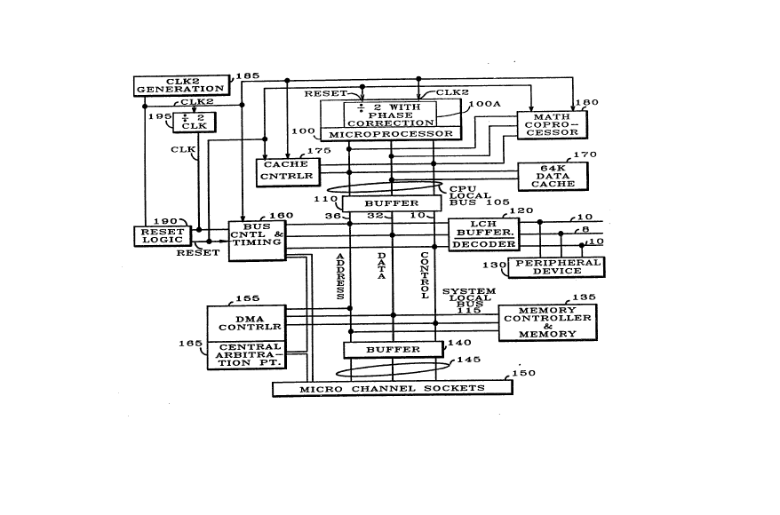
FIG. l i8 a high level block diagram of a conven-
tional dual bus computer.
FIG. 2 18 a timing diagram which ~how~ the relation-
ship between the internal lX clock signal and the external
2X (CLK2) clock ~ignal.
FIG. 3 is a high level block dlagram of the computer
sy~tem of the present invention.
FIG. 4 is a low level, more detailed block diagram
of the reset circuitry portion of the computer system of
FIG. 3.
BC9-89-020 2
2~16401
FIG. 5 is a timing diagram showing the operation of
the reset circuitry of FIG. 4 when no phase error occur~.
FIG. 6. is a timing diagram showing the operation o
the reset circuitry of FIG. 4 when a phase error occur~.
FIG. 7 is a timing diagram employing a time com-
pressed time axis to show the operation of the reset cir-
cuitry of EIG. 4.
RELATED ART
Microprocessors such as the Intel 386 (TM) and i486
(TM~ include a reset input to enable the microprocessor
to be initialized in a known or defined state when power
to the microprocessor is turned on. (386 and i486 are
trademarks of Intel Corporation.) A computer employing
an Intel 386 microprocessor and associated power reset
circuitry i8 shown in FIG. 1 as computer 10. Before dis-
cussing this power reset circuitry, it is helpful to de-
scribe computer 10 in general terms.
Computer 10 is a dual bus computer which includes the
aforementioned microprocessor now designated as micro-
processor 100. Microprocessor 100 includes a reset input
shown in FIG. 1 as RESET. Microproces~or 100 is coupled
via a CPU local bus 105 to a buffer 110 which couple~ CPU
local bu~ 105 to a sy~tem local bus 115. System local bus
115 is coupled via a latch/buffer/decoder 120 to a planar
I/0 (input/output) bus 125 to which peripheral devices
such a~ device 130 are connected. System local bus 115
is further coupled to a memory controller and memory 13S.
BC9-89-020 3
20~6401
System local bus 115 is also coupled via a buffer 140 and
a Micro Channel (TM) bus 145 to Micro Channel (TM) sockets
or slots 150 into which various adapter card~ may be in-
serted. (Micro Channel is a trademark of the Interna-
tional Business Machines Corporation.) A direct memory
access (DMA) controller 15S is coupled to system local bus
115 to facilitate direct access to memory 135 without the
intervention of microprocessor 100. Computer 10 further
includes a bus control and timing circuit 160 which is
coupled to system local bus 115 to permit control and
timing of bus 115. A central arbitration point 165 is
coupled to both bus control and timing circuit 160 Micro
Channel socket~ 150. Central arbitration point 165 de-
termines which functional entity gets access to the Micro
Channel bus 145, be it microprocessor 100, a bus master
plugged into one of Micro Channel sockets 145 or DMA con-
troller 155, for example.
A cache memory 170 is coupled to CPU local bus 105
and microprocessor 100 as shown. To control the operation
of cache memory 170, an Intel 82385 cache controller 175
is coupled to CPU local bus 105 and system local bus 115
as shown. When computer 10 is being referred to as a dual
bus computer, lt is the CPU local bus 105 and the system
local bus 115 which are tha two busses being referenced.
Each of busses 105 and 115 includes respective address,
data and control busses. To facilitate the processing of
floating point operations, a math coprocessor 180 is cou-
pled to CPU local bus 105.
BC9-89-020 4
.
2~6401
As mentioned earlier, microprocessor 100 includes a
reset input designated RESET. Microprocessor 100 further
includes a clock input designated CLK2 to which a clock
frequency of double (2X) the microprocessor internal clock
frequency is provided. The internal clock frequency of
microprocessor 100 is defined to be equal to lX. A divide
by two and phase correction circuit lOOA is included
within microprocessor 100 such that the CLK2 or 2X clock
signal (for example, at 50 MHz) provided to the micro-
processor CLK2 input is divided down to lX (or 25 MHz, for
example) for use internal to microprocessor 100. A CLK2
generation circuit or clock oscillator 185 is provided to
generate the CLK2 signal. CLK2 generation circuit 190
includes a CLK2 output which is coupled to RESET LOGIC
190, a divide by 2 circuit 195, bus control and timing
circuit 160, cache controller 175, microprocessor 100 and
coprocessor 180 to provide clock information thereto.
Reset logic 180 includes a RESET output which is coupled
to the microprocessor RESET input, math coprocessor 180,
cache controller 175 and bus control and timing circuit
160 to provide an appropriate reset pulse to such devices
when system reset is de~ired. From FIG. 1 it is seen that
divider circuit 195 divides the CLK2 clock signal by 2 to
produce an external clock signal designated CLK which is
provided to RESET LOGIC 190 and to bus control and timing
circuitry 160. It is noted that the external clock CLK
signal generated at the CLK output of divider circuit 195
exhibits a frequency substantially the same as the lX in-
BC9-89-020 5
- 2016~01
ternal clock, frequency of microprocessor 100. For this
reason, the CLK signal is referred to alternatively as the
lX external clock signal.
An overview of the operation of the 386 micro-
processor with respect to clocking operations is now pre-
sented. As mentioned above, the 386 microprocessor
operates from a two-times external clock or 2X clock ex-
ternal input. Thus, a 20 MHz 386 microprocessor requires
a 40 MHz external clock ~ignal at its CLK2 input and a 25
MHz 386 microprocessor requires a 50 MHz external clock
signal at its CLK2 input.
Internally, the 386 microprocessor generates its own
one-time (lX) clock by dividing the CLK2 input signal by
two. This lX internal clock signal is used inside the 386
microprocessor to determine the timing of the various in-
ternal logic operations including operations which appear
as microprocessor outputs. This lX clock signal is also
used internal to the 386 microprocessor to determine the
appropriate sample time for external inputs. The timing
relationship of this lX internal clock signal to the CLK2
clock signal is shown in EIG. 2 in which the lX internal
clock signal 1B shown in the lowermost portion thereof and
the CLK2 clock signal iB shown in the uppermost portion
thereof. The timing relationships relative to this lX
clock are documented by Intel in the 80386 Hardware Man-
ual. The lX internal clock signal is used to determine
the appropriate phase of the CLK2 signal since multiple
BC9-89-020 6
2016~01
CLK2 phases are re~uired to complete a 386 microprocessor
bus cycle.
The typical 386 microprocessor based computer 6ystem
will generate, external to the 386 microprocessor, its own
lX external clock signal since there i8 no lX external
clock output from the 386 microprocessor. A~ seen in FIG.
1, thiæ external lX clock signal is generated in computer
lO at the CLK output of divider circuit 195 as the CLK
signal is. This lX external clock signal or CLK signal
is used by external logic to monitor or sample the 386
microprocessor and to control the necessary 386 micro-
processor inputs.
The two separately generated lX clocks, namely the
internal lX clock and the external lX clock ~CLK at di-
vider 195) may undesirably differ in their phasing unless
some means is provided to achieve synchronization of the
internal lX clock and the external lX clock during the
power up of microprocessor lOO. This required synchroni-
zation action is typically provided by generation of the
signal RESET which is provided to the RESET input of mi-
croprocessor lOO. External logic, namely reset logic l9O,
triggers the active edge of the RESET signal relative to
the externally generated lX clock. That is, there i8
known and fixed relationship between the active edge of
the RESET signal and the externally generated lX clock
signal. The RESET signal is sampled by the 386 micro-
processor on each CLK2 rising edge. The resulting RESET
sample information is used by internal divide by 2 and
BC9-89-020 7
2016401
phase correction circuitry lOOA to change the phasing of
the internal lX clock if required to bring the internal
lX clock into ~ync with the external lX clock.
To provide the computer user with a proce~sor upgrade
path in one type of computer 10, a daughter card (not
shown) is provided which includes microprocessor 100, co-
processor 180, cache controller 175, cache 170 and the
associated reset circuitry. This daughter card is alter-
natively referred to as a processor complex. The daughter
card plugs into a planar board or motherboard containing
the remaining components and devices of computer 10 shown
in FIG. 1. In this manner, a daughter card containing a
different microprocessor configuration than that ori-
ginally provided with computer 10 can be plugged into the
planar board to improve computer performance. An example
of one computer employing such a daughter card arrangement
is the IBM Personal System/2 Model 70 A21 computer.
(Personal System/2 is a registered trademark of the In-
ternational Business Machines Corporation.)
Microprocessor technology ha~ advanced beyond the
level of the 386 based computer lO described above. More
specifically, Intel Corporation has recently introduced
the i486 microprocessor which offers significant processor
performance benefits by incorporating a microprocessor,
coprocessor, cache memory and cache controller on a single
chip.
Unfortunately, a number of difficultie~ are encount-
ered when attempting to outfit an existing computer such
BC9-89-020 8
2~16401
as computer 10 with a i486 microprocessor. It will be
recalled that computer 10 include~ an e~ternal 2X clock
(CLK2), and the 386 microprocessor of computer 10 includes
a CLK2 pin to which the 2X clock signal is provided. The
386 microprocessor further include~ an internal divide by
2 circuit to produce an internal lX clock. In contrast,
the i486 microprocessor does not use the same internal
clock phase setting approach via the microprocessor RESET
pin as does the 386 microprocessor, but rather the i486
; microprocessor employs a simple lX clock pin. This means
that a 25 MHz i486 operates from a 25 MHz clock input.
In further contrast to the 386 microprocessor, the i486
microprocessor uses an internal frequency doubling circuit
to generate an internal 2X clock.
Due to thi~ arrangement, the i486 microprocessor as-
sume~ that the proper CLK phasing is implicit in the one-
times (lX) CLK pin input to the i486. Thus, the i486
microprocessor does not sample its RESET input to achieve
clock pha3e correction. This difference in RESET/CLK
phasing between the 386 microprocessor and the i486 mi-
croprocessor causes lX clock synchronization difficulties
j in an application where a processor upgrade from a 386
microprocessor to an i486 microprocessor is attempted,
j when minimal change to the remaining circuitry of computer
10 or other computer is desired.
.
BC9-89-020 9
2016401
DETAILED DESCRIPq~ION OF T~IE INVENTION
FIG. 3 is a high level block diagram which
depicts the computer system of the present invention
as computer system 200. Computer system 200 has
elements in common with computer system 10 of FIG. 1
with the exception of the modifications shown in FIG.
3 and now discussed. Like numerals are used to
indicate like elements in FIG. 3 and FIG. 1.
In the preferred embodiment of the invention,
computer system 200 includes an i486 microprocessor
designated microprocessor 205 having a lX clock input
designated CPUCLK and a reset input designated
MPRESET input as shown in FIG. 3. The internal clock
frequency of microprocessor 205 is defined to be
equal to lX and the frequency of the clock signal
provided to the CPUCLK input is also lX.
Microprocessor 205 is coupled to CPU local bus 105 as
shown. The CLK~ output of CLK2 clock signal
generation circuit 185 is coupled to the CPUCLK clock
input of microprocessor 205 via a divide by two with
phase correction circuit 210. The CLK2 output of
CLK2 generation circuit 185 is also coupled to a time
base input or clock input ~DCLK2, CLK2C) of the input
of a phase checker circuit 215 via a time delay
circuit 212. In this manner, a time delayed version
of the CLK2 clock signal, namely the DCLK2 signal,
which is produced at the DCLK2 output of time delay
circuit 212, is provided as the time base for phase
checker 215. The DCLK2 output of time delay circuit
212 is also coupled to a time base input of reset
logic circuit 190 such that the same delayed clocking
information or time base signal DCLK2 is provided to
2016~01
. .
phase checker 215 and reset logic 190.
Phase checker circuit 215 includes phase inputs
215A and 215B and a phase error output designated
PHERR at which a phase error signal PHERR is
generated which represents the phase error between
signals (later described) which are provided to phase
inputs 215A and 215B. The CPUCLK output of divide by
2 with phase correction circuit 210 is coupled via a
time delay circuit 217 to phase input 215A of phase
checker 215 such that a delayed version of the CPUCLK
signal (DCLK) produced at the output of delay circuit
217 is provided to phase input 215A.
The RESET output of RESET logic circuit 190 is
coupled to the remaining phase input 215B of phase
checker 215 to provide reset pulse phase information
thereto. Providing the DCLK and RESET signals to
phase inputs 215A and 215B in this manner permits
phase checker 215 to compare the phase of the delayed
CPUCLK signal (DCLK) with the implicit phase of the
RESET signal. If phase checker 215 detects a phase
error between the DCLK signal and the RESET signal,
then phase checker 215 generates a phase error signal
PHERR at the PHERR output of phase checker 215. This
phase error indicates that an undesirable phasing
relationship exists between the CPUCLK signal (as
represented by DCLK) and the CLK signal provided by
divider 195. The PHERR output of phase checker 215
is coupled to the PHERR input of divided by 2 with
phase correction circuit 210 to provide the PHERR
signal thereto. The PHERR signal is also provided to
the PHERR input of a reset regeneration generation
circuit 220 which is discussed later.
Although phase checker 215 is checking the phase
11
201~401
of the CPUCLK signal (as represented by DCLK) with
respect to the RESET signal, it effectively checks
the phase of the CPUCLK signal (internal
microprocessor clock) with xespect to the phase of
the external clock signal cLK generated at the output
of divider 195. This i8 SO because the falling edge
of the RESET signal generated by reset logic 190
contains clocking information with respect to the CLK
external clock signal, since reset logic 190 follows
the earlier timing convention compatible with the 386
microprocessor.
If phase checker 215 determines that a phase
error exists between the delayed CPUCLK signal (DCLK)
and the RESET signal such as during power up of
microprocessor 205, then a PHERR signal is generated
which drives divide by 2 with phase correction
circuit 210 to bring the delayed CPUCLK signal (DCLK)
into phase with the RESET signal. In this manner the
phase of the CPUCLK signal is adjusted and corrected.
However, when such a phase adjustment occurs, the t
clock stability specification of the i486
microprocessor is violated as discussed later in more
detail~ When such a specification violation occurs,
then reset regeneration circuit 220 regenerates or
produces a new reset signal pulse (NEWRESET) which is
provided to the MPRESET input of microprocessor 205
to reset microprocessor 205. As seen in FIG. 3, the
RESET output of RESET logic 190 is coupled to the
RESET input of RESET regeneration circuit 220 to
provide the RESET signal thereto. Reset regeneration
circuit 220 includes a RCLK output which is coupled
to an input of a timing element 225, such timing
element 225 including an RCNT6 output which is
:. .
2016401
coupled back to reset regeneration circuit 220 as
will be explained later. The PHERR output of phase
checker 215 is coupled to a PHERR input of reset
regeneration circuit 220 to inform reset regeneration
circuit 220 as to when regeneration of the reset
signal is required. In this manner, reset
regeneration circuit 220 is informed as to when the
generation of the NEWRESET pulse is needed. It is
noted that supplying this NEWRESET pulse to the RESET
input of microprocessor 205 results in microprocessor
205 desirably being returned to an known state.
FIG. 4 is a lower level, more detailed block
diagram showing the reset circuitry portion of
microprocessor based computer system 200. In
comparing the diagrams of FIG. 4 and FIG. 3, it will
be noted that some signals, inputs and outputs have
been renamed or are given alternative names as
explained subsequently or as shown by the labelling
in FIG. 4. This has been done to facilitate the
implementation of the reset circuitry portion in
programmable array logic or PAL form as will be
explained in more detail later. (PAL is a registered
trademark o~ Monolithic Memories, Inc.) Signals
which are generated and used internally within the
various blocks of FIG. 4 are shown in parenthesis.
The signals employed in the reset circuitry
portion of FIG. 4 are the same as the signals in the
reset circuitry portion of FIG. 3 except for the
differences subsequently discussed. The CLK2 signal
generated at the output of CLK2 clock signal
generator 185 is also referred to as CLK2ALSO. The
DCLK2 signal produced at the output of delay element
212 is alternatively designated CLK2A, CLK2B and
~Q~401
CLK2C. The CPIJCLK signal produced at the output of
divide by 2 with phase correction circuit 210 is also
referred to as CLK and CLKX. The RESET signal
generated by reset logic 190 is shown in more detail
in the reset circuitry of FIG. 4 as including a
CPURESET signal which is supplied to reset
regeneration logic 220 and further including a
CACHERESET signal which is provided to reset
regeneration logic 220 and phase checker 215.
A delayed version DPHERR of the phase error
signal PHERR is generated internal to the divide by 2
with phase correction circuit 210 as shown in FIG. 4
and indicated in parenthesis. A CRESETSYNC signal is
generated internal to phase checker 215 and is
supplied to timing element 225. CRESETSYNC is a
delayed and inverted version of the CACHERESET signal
generated by reset logic 190.
In one embodiment of the invention, timing
element 225 is a 74LS590 counter manufactured by
Texas Instruments, Inc. This timing element is used
to determine the required pulse width of the NEWRESET
pulse, such pulse width being approximately 1
millisecond.
An input signal BHOLD is provided to reset
regeneration circuit 220 as seen in FIG. 4.
BHOLD is employed as an accessible timing signal
which pulses once every approximately 15.6
microseconds and is used to generate the clock pulse
for counter of timing element 225. RCLK is derived
from BHOLD and is provided to timing element 225 as
will be discussed later.
Divide by 2 with phase correction circuit 210,
delay circuit 217 and delay circuit 212 are
2016401
conveniently fabricated in a first PAL device as
specified by the following PAL inputs, outputs and
logic equations. In the subsequent logic eguations,
the following symbols have the meaning designated
below:
SYMBOL DEFINITION
/ Negation
:= A registered term, equal to
= A combinatorial term, equal to
& Logical AND
+ Logical OR
The first PAL device is defined to exhibit the - -
following input pins:
INPUT PIN COMMENT
CLK2 - 50 MHz TTL oscillator
CLKALSO - 50 MHz TTL oscillator
PHERR - phase error
The first PAL is defined to exhibit the following
output pins:
OUTPUT PIN COMMENT
CLK2A - 50 MHz buffered CLK2
DCLK - delayed 25 MHz clock
CLK - 25 MHz clock to i486 and PALS
DPHERR - phase error pulse
CLKX - 25 MHz clock to i486 and PALS
CLK2C - 50 MHz buffered CLK2
CLK2B - 50 MHz buffered CLK2
``- 201 6401
.. .... .
The following logic equations describe the logic
implementation within the fi.rst PAL device:
CLK2A = CLK2ALSO
CLK2B = CLK2ALSO
CLK2C = CLK2ALSO
!CLK := (CLK & PHERR)
# (CLK & !PHERR & !DPHERR)
!CLKX := (CLK & PHERR)
# (CLK & !PHERR & !DPHERR)
!DPHERR:= (!PHERR & CLK)
# (!DPHERR & !CLK)
DCLK = CLK
,
Phase checker 215 and reset regeneration logic
220 are conveniently fabricated in a second PAL
device as specified by the following PAL inputs,
outputs and logic equations. Accordingly, the
second PAL device is defined to exhibit the following
input pins:
INPUT PIN COMMENT
CLK2C - 50 MHz TTL CLK2
DCLK - 25 MHz delay CPU clock
CACHERESET - cache reset pulse
CPURESET - CPU reset pulse
HOLD - CPU hold request
RCNT6 - reset counter bit 6
16
. . - -
2~6401
The second PAL is defined to exhibit the following
output pins:
OUTPUT PIN COMMENT
NEWRESET - new CPURESET including phasing
RCLK - reset counter clock
PHEM - phase error pulse
CRESETSYNC - delayed and inverted CACHERESET
RCNTSYNC - sampled version of input RCNT6
The following logic equations describe the logic
implementation within the second PAL device.
!CRESETSYNC := CACHERESET
NEWRESET := CPURESET
# !PHERR & !CACHERESET
# NEWRESET & !RCNTSYNC & CRESETSYNC
& !PHERR
' !PHEM := DCLK & !CRESETSYNC & !CACHERESET
#!PHERR & !RCNTSYNC & !CACHERESET
# !PHERR & !DCLK
!RCLK := !DCLK & !PHERR & CRESETSYNC & HOLD
#RCLK & !DCLK & CACHERESET
# !RCLK & DCLK
RCNTSYNC := RCNT6 & !DCLK
# RCNTSYNC & DCLK
FIG. 5 is a timing diagram which shows the
operation of the reset circuitry of FIG. 4 by
illustrating the CLK2/CLK2ALSO, CACHERESET, RCNT6,
CLK2C, CRESETSYNC, PHEM, DPHERR, CLK/CLKX/, CPUCLK,
DCLK, NEWRESET, RCLK, CLK2A, BHOLD and CPURESET
signals of sUch reset circuitry on a common time
axis. FIG. 5 illustrates the case where no phase
error occurs as seen by observing the consistently
17
20164~1
high PHERR signal.
FIG. 6 is a timing diagram which shows the
operation of the reset circuitry of FIG. 4 by
illustrating the CLK2/CLK2ALSO, CACHERESET, RCNT6,
CLK2C, CRESETSYNC, PHERR, DPHERR, CLK~CLKX/, CPUCLK,
DCLK, NEWRESET, RCLK, CLK2A, BHOLD and CPURESET
signals of such reset circuitry on a common time
axis. FIG. 6 illustrates the case where a phase
error occurs as observed at the falling edge of the
PHERR signal at 300. The reset circuitry corrects
this phase error as seen at the lengthened CLK pulse
at 305.
FIG. 7 is a timing diagram which shows the
operation of the reset circuitry of FIG. 4 by
illustrating the CLK2/CLK2ALSO, CACHERESET, RCNT6,
CLK2C, CRESETSYNC, PHERR, DPHERR, CLK/CLKX/, CPUCLK,
DCLK, NEWRESET, RCLK, CLK2A, BHOLD and CPURESET
signals of such reset circuitry on a common time axis
over a longer duration of time than in the timing
-
diagrams of FIG. 5 and FIG. 6 by compressing the time
axis. The timing diagram of FIG. 7 illustrates how
the RCLK and BHOLD signals operate to time out the
counter within timing element 225. RCNT6 provides
the return signal from this counter. As illustrated
in FIG. 7, for convenience of presentation, BHOLD
pulses at less than the previously stated 15.6
microsecond rate, and RCLK is counted for only two
counts here instead of 2' counts as it does in actual
practice in one embodiment of the invention.
The following is a summary of the operation of
the reset circuitry portion of computer system 200 of
FIG. 3 and FIG. 4. When computer 200 is initially
powered up or when reset logic 190 is otherwise
18
2016401
instrueted to generate a reset pulse, reset logic 190
generates an initial reset pulse designated RESET.
The initial reset pulse RESET is supplied to reset
regeneration circuit 220 whieh passes this initial
RESET pulse on to mieroprocessor 205 via the NEWRESET
line whieh is later used to transmit the NEWRESET
pulse to microprocessor 205. Thus, the initial RESET
pulse eauses mieroproeessor 205 to exeeute an
internal mieroprocessor reset operation. This
lo initial RESET pulse is also provided to phase ehecker
215 which uses this RESET pulse in the manner
described below in the discussion of phase checker
215.
The logic provided in the reset circuitry
performs a divide by two operation at divider/phase
corrector 210 on the CLK2 clock signal of the CLK2
generator which exhibits a 2X cloek frequency to
provide microprocessor 205 with an appropriate cloek
signal exhibiting a lX elock frequeney at the CPUCLK
input thereof. Phase ehecker 215 then determines if
a phase error occurs between the CPUCLK signal and
the RESET signal generated by reset logie 190. (The
RESET signal carries indicia of the phase of the CLK
lX external eloek signal.) Sueh a phase error is
typieal at mieroproeessor power up. If sueh a phase
error is deteeted, then the phase of the CPUCLK
signal is eorrected by divider/phase eorreetor 210.
However, when the phase of the CPUCLK signal is so
eorreeted and shifted, the Intel timing speeifieation
for the i486 elock stability is violated (tl,
speeification is .1% maximum change between adjacent
CPUCLK clock pulses).
If a corrective CPUCLK phase shift i5 required,
19
2016401
then reset regeneration circuit 220 generates a new
reset pulse NEWRESET which is supplied to the MPRESET
input of microprocessor 205 to reset microprocessor
205 to a known state. In other words, if a CPUCLK
phase shift is required due a detected phase error,
the MPRESET input of microprocessor 205 is redriven
to its active state and held there for a full reset
interval (approximately 1 millisecond), thus clearing
any errors internal to microprocessor 205 caused by
lo the CPUCLK phase error.
Additional operational details of the reset
circuit of FIG. 3 and FIG. 4 are now discussed
together with a summary of the various signals or
terms employed in the reset circuit of FIG. 4. The
output terms CPUCLKA, CPUCLKB and CPUCLKC shown in
FIG. 4 are delayed versions of the CLK2 clock signal
from CLK2 generator 185. The terms are employed to
compensate for time delays resulting from
divider/phase corrector 210. The time delay element
212 used to generate these terms assures minimal
skewing of the timing requirements in the remainder
of the system circuitry.
CLK and CLKX in FIG. 4 are duplicate versions of
the divided by 2 or lX CPUCLK signal which is used to
clock microprocessor 205. DCLK is a time delayed
version of the CPUCLK, such DCLK signal being one
input to phase checker 215 as already described.
DPHERR is a logic term used internally to
divider/phase corrector 210 in setting the proper
phase of CPUCLK, CLK and CLKX. It is noted that the
output PHERR will go active (low) if a phase error is
detected between the CPUCLK signal (as represented by
DCLK) and the RESET (CACHERESET) signal provided to
.. - . , . ~ ... . -
20164 01
phase checker 215. As discussed above, the phase
error signal PHERR is employed in reset regeneration
circuit 220 to drive the NEWRESET signal active
(high) into the MPRESET input of microprocessor 205
thus returning microprocessor 205 to a known state.
As seen in FIG. 3, the central arbitration point
includes a bus hold request output B~OLD. When the
aforementioned phase error is detected, depending on
the timing of the BHOLD signal, output RCLK will
pulse low, following the state of the BHOLD signal
(inverted). The BHOLD signal, shown in FIG. 4 as
being provided to reset regeneration logic 220, is
employed as a timer signal. In this particular
embodiment of the invention wherein CPUCLK exhibits a
frequency of 25 MHz, the BHOLD signal pulses once
every approximately 15.6 microseconds~ These BHOLD
pulses pulse the RCLK output of reset regeneration
logic 220. This action in turn increments the
74LS590 counter in timing element 225 once every
approximately 15.6 microseconds. This counter
increments for 27 counts, yielding a total of
approximately 1 millisecond, before the 27 counter
bit connected to RCNT6 goes active. When this timer
bit RCNT6 goes active, it is employed to deactivate
the NEWRESET signal, the generation of which was
described earlier. In this manner, the duration of
the NEWRESET pulse is controlled and set. After
NEWRESET goes inactive, both the microprocessor 205
and the remainder of computer system 200 are
synchronized and operation of computer system 200 can
begin.
The terms CRESETSYNC and RCNTSYNC are used
internally within the PAL logic implementation of the
201~401
reset circuit of FIG.'s 3 and 4. Additionally,
CRESETSYNC is used externally to clear the 74LS590
counter to its initial zero count.
While a computer system reset circuit apparatus
has been described above, it will be appreciated that
a method for resetting a microprocessor has also been
disclosed. Such method is employed in a computer
system including a microprocessor, such
microprocessor exhibiting a reset input and further
lo exhibiting a clock input to which a clock signal is
provided. The computer system in which the method is
practiced is capable of generating a microprocessor
reset signal. More specifically, a method for
resetting the microprocessor in such system is
disclosed and includes the step of detecting a phase
error between said clock signal and the reset signal.
The method further includes the step of adjusting the
phase of the clock signal if a phase error is
detected so as to substantially minimize the phase
error. The method also includes the step of
providing a new reset signal to the reset input of
the microprocessor in the event that the phase of the
clock signal is adjusted.
The foregoing has described an apparatu~ and
method for resetting the reset input in a
microprocessor based computer system. The apparatus
and method disclosed provides reset circuitry which,
in one embodiment of the invention, permits an i486
microprocessor to operate in a computer which
originally employed a 386 microprocessor. The
apparatus and method provides reset circuitry which
requires minimal change to the circuitry of a 386
microprocessor computer when such computer is
2016~01
upgraded with an i486 microprocessor. In one
embodiment of the invention, the apparatus and method
desirably overcomes reset timing difficulties
experienced in a computer system in which a processor
upgrade from a 386 microprocessor to an i486
microprocessor is attempted.
While only certain preferred features of the
invention have been shown by way of illustration,
many modifications and changes will occur to those
skilled in the art. It is, therefore, to be
understood that the present claims are intended to
cover all such modifications and changes which fall
within the true spirit of the invention.