Note: Descriptions are shown in the official language in which they were submitted.
CA 02016497 1997-11-26
SONET TRANSMIT SIGNALING TRANSLATOR
BACKGROUND OF THE INVENTION
Field of the Invention
The present invention relates to telephone
signaling, and more particularly, to a device for translating
channel-associated signaling, of the type wherein the
signaling bits for each data channel are associated with each
other and with their corresponding data, into SONET-formatted
signaling.
Description of the Prior Art
The American National Standard Institute, Inc.
(ANSI) T1.105-1988 describes the Synchronous Optical Network
(SONET) protocol for telecommunications equipment. The SONET
protocol is particularly adapted for optical transmission, and
various transmission levels have been standardized at
specified line rates in M bit/s. The first level, Optical
Carrier Level 1, or OC-1, transmits data at the rate of 51.84
M bits/s. This carrier level has a corresponding electrical
level called Synchronous Transport Signal Level 1, or STS-1.
In order to access this high-frequency carrier
level, access products are required so that lower bandwidth
carriers can be introduced into or extracted from the STS-1
transmission level. These access products provide a SONET
network with nodes where components of an STS-1 signal can
-- 1 --
65993-191
~Q16~7
be added to or dropped out of the main signal. The
components that are extracted must be reorganized to produce
a signaling format compatible with currently-used telephone
standards. In like manner, components that are added must
have their signaling reorganized for insertion into the
SONET format. A typical sub-component of an STS-1 signal
would be a DSl signal having a bit rate of 1.544 M bits/s.
Twenty-eight DS1 signals can be supported by an STS-1
carrier. Within the DS1 signal format, an additional 24 DSO
64K bits/s signals can be supported.
The SONET transmission is serial, comprising a total of
810 bytes. The frame structure for an STS-1 is shown in
Figure 1. The frame comprises 90 columns x 9 rows of bytes,
with 8 bits per byte. The sequence of transmission of the
bytes is row by row, from left to right. The frame is
divided into three parts: the section and line overhead,
which are contained in the first three columns; and the
payload, which is found in the 87 remaining columns, which,
in connection with the nine rows, forms a Synchronous
Payload Envelope, SPE, which includes 783 bytes. Nine of
the SPE bytes are allocated to path overhead. The SPE can
begin anywhere within the 87 x 9 byte envelope. Typically,
the SPE begins in one SONET frame and ends in another. A
payload pointer provided in overhead bytes H1 and H2 points
to the byte where the SPE begins, shown as P=O in Figure 1.
The information within the SPE is transported in Sub-STS-l
payloads called Virtual Tributaries, or VTs. There are
several levels of VTs; however, it is only necessary to deal
with a VT 1.5 for purposes of describing this invention.
When the STS-l payload supports 28 DSl services, one VT at
the 1.5 level is provided for each DS1 service.
Figure 2 illustrates the payload mapping of SONET bytes
into a DS1.
~164~7
An SPE consists of 783 bytes belonging to 28
tributaries, wherein each tributary can carry a DSl payload,
as illustrated in Figure 2. A DSl payload has 27 bytes, 24
of which carry DS0 channels. The first byte carries a VT
pointer, or address; a second byte is unused; and the third
byte carries signaling data for the DSl payload. Every
channel has four signaling bits, namely, A, B, C and D, as
is well known in the telephony art. Thus, for a DSl payload
of 24 channels, a total of 96 signaling bits are required.
Since only four bits of signaling are carried in each SONET
signaling byte and there is only one signaling byte per
tributary or DSl, a total of 24 SONET frames would be
required in order to transmit the 96 required signaling
bits.
Figure 3 illustrates the transmission order of the
payload contained within the SPEs of 24 SONET frames. For
the sake of clarity, a number of bytes of the SPE are now
shown in Figure 3. These bytes include: the first two rows
of each SPE, which would contain bytes 1 and 2 of each of
the 28 tributaries, as shown in Figure 2, the nine path
overhead bytes, and additional 'fixed stuff' bytes. In
addition, the SPE has been shown as being located entirely
within one SONET frame. This facilitates the illustration
in Figure 3 of the signaling bits provided in each SPE
byte. Thus, the first row of each frame shown in Figure 3
is the signaling row and contains byte number 3 for each of
the tributaries. The transmission order proceeds from left
to right in each descending row of a frame. Thus, bytes
containing four signaling bits for tributaries 0-27 are
transmitted in sequence, after which the data for channels 0
for each tributary is transmitted, followed by the data for
the other channels through to the transmission of the data
for channels 23.
2~1&~7
Due to the presence of nine overhead bytes (not shown),
bytes 1 and 2 of each tributary, and additional unused
'fixed stuff' bytes in the SPE, the signaling bytes start
with SPE byte 60 and continue through byte 87. The content
of each SONET signaling byte is as follows:
(MSB) (LSB)
Bit No. 7 6 5 4 3 2 1 0
Byte Sync R R Sl S2 S3 S4 F R
Bit Sync 1 0 R R R R F R
R bits are not used
In the above, Sl, S2, S3 and S4 are the signaling bits
corresponding to the sets of four bits shown in the
signaling bytes in Figure 3. Thus, the signaling bits
transmitted in the SONET signaling rows of sequential frames
are transmitted in the order of all A bits, all B bits, all
C bits and all D bits, which bits;are not associated with
their corresponding channel data and the A, B, C and D bits
from a channel are not associated with each other.
Commonly used telephony signaling systems include
systems wherein the signaling bits are transmitted inband
within the channel data, and other systems transmit the
signaling bits in separate signaling channels. However, in
most cases the signaling bits for a channel are associated
with each other or are transmitted in association with the
channel data. Thus, a system was required which could
extract the signaling information from lower-level telephone
transmission lines and reassemble the signaling bits into a
format which would facilitate insertion of the bits into the
SONET format shown in Figure 3. A total of 2,688 signaling
bits must be transmitted on the SONET STS-l carrier, and
these bits must be accumulated from the 24 channels of each
2~ g~
of the the 28 DS1 carriers supported by the STS-1
transmission level, with each channel having A, B, C and D
signaling bits. There are no known solutions to the problem
of translating signaling data from the standard signaling
formats into the SONET format.
In the system for which this invention was designed, a
16-bit internal byte was used for each channel, with each
bit being provided on a separate line of a parallel bus.
Thus, for each clock pulse a complete byte of channel
information was obtained. The internal signaling format for
a 16-bit byte is compared to a SONET data byte as follows:
PDO
PD15
Internal ¦D7¦D6¦D5¦D4¦D3¦D2¦D1¦D0¦ A ¦ B ¦ C ¦ D
¦MFS¦MFS2¦ ¦P¦
Byte ll
v v v v v v v v
¦MSB Data Field LSB¦ Signal Field
¦MSB LSB¦
SONET ¦D7¦D6¦D5¦D4¦D3¦D2¦D1¦DO¦
Byte
It is to be noted that the internal byte includes a full
eight bits of data, which bits are directly transferable to
a SONET data byte. The signaling bits A, B, C and D are
located out of the data band and therefore do not
deteriorate the transmitted data.
The STS-l SONET format handles 672 data channels, each
with ABCD signaling, for a total of 2,688 signaling bits.
These bits are available in every internal 125 u sec frame
time and are provided in the four outband bit positions.
These signaling bits, provided in the same byte as the
2~164g7
internal data, must be extracted from the internal byte and
rearranged for insertion into the SONET format.
The access products used to extract and add sub-
components to the STS-1 transmission level include both an
add-drop multiplexer and a terminal multiplexer. The
terminal multiplexer receives and extracts all data from the
STS-l and inserts new data in a return path. The add-drop
multiplexer, however, poses special problems, since it
facilitates the extraction and/or addition of any number of
channels carried on the STS-l line. Thus, some channels
pass directly through an add-drop multiplexer, while some
channels are extracted and other channels are added.
All received channel signaling is converted to the internal
format. Thus, the through channels could be treated
similarly to the add channels by reconstructing the SONET
signaling format from the outband signals provided in the
internal format. However, this would cause unnecessary
delay for through channels, as the signaling is processed by
the access product. Preferably this delay should be avoided
by passing each tributary signaling byte through the
multiplexer and only overwriting the signaling bits that are
being added.
SUMMARY OF THE INVENTION
The present invention contemplates a signaling
translator that translates telephone signaling provided as
channel-associated signaling to a signaling format for use
in 8-bit SONET bytes. An internal 16-bit byte format makes
four signaling bits available in each channel (DSO) time
slot. In every internal 125 usec frame, 2,688 signaling
~16497
bits are available, but only 112 are needed for insertion
into the SONET frame.
In a terminal multiplexer application, signaling bits
are provided for each signaling byte of the SONET frame. In
an add-drop multiplexer, only signaling bits for channels
added to the SONET transmission line are inserted, while the
signaling bits for other channels are passed through the
multiplexer. Thus, signaling bits for through channels
merely pass through the translator, while signaling bits for
added channels are multiplexed with the through channels to
provide the signaling bits for a SONET frame.
A memory provisioned by a network control processor
stores one bit for each channel to provide an indication as
to whether the channel is an add channel or a through
channel. This memory is addressed for controlling the
multiplexer, which selects the signaling for the through
channels or the signaling for the add channels.
In each frame period selected outband signal bi~s are
shifted into four shift registers for providing four output
bits in the SONET format. These output bits are multiplexed
with the through signal bits of the SONET byte to provide an
output for insertion into the appropriate SONET signaling
bytes.
A primary objective of the present invention is to
provide a signaling translator for a SONET STS-1
transmission interface.
Another objective of the present invention is to
provide a device which rearranges channel-associated
signaling into a SONET format for insertion into a SONET
frame.
d~ q7
65993-191
Another objective of the present invention is to provide
a SONET access product which passes channel signaling through the
product while multiplexing in signaling relating to channels added
by the access product.
Another objective of the present invention is to provide
a signaling translator that is useful in both add-drop multiplexer
and terminal multiplexer access products.
Another objective of the present invention is to provide
a signaling translator that is provisionable by a processor to
pass the signaling for selected channels through the translator,
while multiplexing in signaling for other channels.
Another objective of the present invention is to provide
a signaling translator that passes signaling of through channels
through the access product without delay.
The invention may be summarized, according to one
aspect, as a device for interfacing a high-frequency SONET-
formatted carrier, of the type that transmits information in
channels associated with tributaries, with a lower bandwidth
carrier, of the type that transmits information in lower-level
transmission channels, said device including: means for receiving
signaling bits from said lower-level transmission channels of the
lower bandwidth carrier; and means for translating said received
signaling bits from said lower-level transmission channels into
SONET-formatted signaling bits.
According to another aspect, the invention provides a
device for interfacing a high-frequency SONET-formatted carrier of
the type that transmits information in channels associated with
.. 8
eLlC17
65993-191
tributaries, with a lower bandwidth carrier, said device
including: means for translating signaling bits associated with
lower-level transmission channels into SONET-formatted signaling
bits; means for receiving SONET-formatted signaling bits from said
high-frequency SONET-formatted carrier; and means for selecting,
for each channel of said channels associated with tributaries,
SONET-formatted signaling bits from either said means for
translating or said means for receiving, and for outputting the
selected SONET-formatted signaling bits.
According to yet another aspect, the invention provides
a SONET access product wherein selected ones of received SONET
channels are passed through the access product while other SONET
channels are added from lower-level transmission systems by the
access product and channel-associated signaling of the added
channels is rearranged into SONET-formatted signaling, said access
product comprising: means for rearranging channel-associated
signaling into SONET-formatted signaling for all lower-level
transmission channels connected to said access product; means for
receiving all SONET-formatted signaling for all SONET channels
received by said access product; an output for SONET-formatted
signaling for all SONET channels; multiplexing means connected to
receive SONET-formatted signaling from said means for rearranging
and connected to receive SONET-formatted signaling from said means
for receiving all SONET-formatted signaling and for providing at
an output a selected one of said SONET-formatted signaling for
each channel of the SONET channels in response to a control
signal; and means for providing a control signal to said
.0-, 9
~DIl~4q~
65993-191
multiplexing means for each SONET channel indicating whether the
SONET channel is a passed through channel or an added channel.
According to still another aspect, the invention
provides a device for interfacing a high-frequency SONET-formatted
carrier, of the type that transmits information in channels
associated with tributaries, with a lower bandwidth carrier, of
the type that transmits information in lower-level transmission
channels, said device including: means for receiving signaling
bits from said lower-level transmission channels of the lower
bandwidth carrier; means for selectively reading a type of said
signaling bits from sequential channels of said lower-level
transmission channels; a plurality of shift registers, each for
storing bits of the selected type of signaling bit for a
predetermined one of said channels, associated with tributaries,
for each tributary of the SONET-formatted carrier; means for
writing the bits of the selected type of signaling bit for each
predetermined channel sequentially into the shift registers; a
plurality of parallel outputs; and means for reading out said
shift registers to said plurality of parallel outputs, whereby
each output sequentially provides signaling bits of the selected
type for one of said predetermined channels associated with
tributaries, one bit for each tributary for transmission in a
frame of SONET-formatted signaling bits, whereby said received
signaling bits from said lower-level transmission channels are
translated into SONET-formatted signaling bits.
DESCRIPTION OF THE DRAWINGS
Figure 1 shows the format of an STS-1 SONET frame.
a~ q7
65993-191
Figure 2 shows the payload mapping of the DS1
transmission line.
Figure 3, comprising Figures 3A and 3B, shows a portion
of a SONET Synchronous Payload Envelope (SPE) and the relationship
of signal bits to sequential SONET frames.
Figure 4 shows schematically the operation of an add-
drop multiplexer.
Figure 5 is a block diagram showing the signaling
translator of the present invention.
Figure 6 is a schematic diagram of a random access
memory (RAM) control circuit.
Figure 7 is a schematic diagram of a signal memory
circuit.
Figure 8, comprising Figures 8A and 8B, is a schematic
diagram of a 28-bit shift register used in the signal memory of
Figure 7.
Figure 9, comprising Figures 9A and 9B, is a schematic
diagram of a signal memory decoder circuit.
Figure 10 is a schematic diagram of an output
multiplexer.
Figure 11 is a schematic diagram of a flip-flop used in
the shift register of Figure 8.
DESCRIPTION OF THE INVENTION
Figure 4 shows schematically the function of an add-drop
multiplexer 10, wherein an STS-1 level transmission is received at
an input 12 in the SONET format, while the sub-components
contained therein are provided at an output 14 for connection to
9b
q 1
65993-191
DS1/DS0 interface circuitry. Channels to be added to the STS-1
SONET transmission are provided at an input 16 in a DS1/DSO
format. The SONET frame is passed through the add-drop
multiplexer to an output 18, where the added channels provided at
input 16 are multiplexed with the SONET channels so that the added
channels replace the channels of the received SONET frame. In a
terminal multiplexer all channels are provided to output 14, and
all channels are provided to input 16, and no channels pass
through from input 12 to output 18.
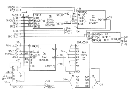
Figure 5 shows a block diagram of the signaling
translator for mapping signaling contained in the channels added
at input 16 of Figure 4 into the signaling of SONET frames
received at input 12. The STS-1 transmission is formatted in
frames as shown in Figure 1. The SPE of the SONET frames is
arranged in part as shown in Figure 3. The
~b 9 C
2~1~497
added channels provided at input 16 of Figure 4 are
formatted as 16-bit words.
In a terminal multiplexer, all channels are provided at
input 16 and thus in a single internal frame period of 125
usec, 2688 signaling bytes are made available, of which 112
are selected to be inserted in each signaling row of the
SONET format outputted at 18.
The signaling translator shown in Figure 5 comprises a
random access memory (RAM) 20 which is organized as a 256 x
4 bit memory, of which 192 locations are used to store 672
bits of data, one bit for each channel transmitted at the
STS-1 level. RAM 20 includes eight address inputs connected
to an address bus 22, a write-enable input 24, four data
inputs connected to a data bus 26, and four data outputs
connected to an output bus 28. The content of RAM 20 is
shown in Table 1, which illustrates how 168 RAM addresses
are used to store a total of 672 bits, one for each
channel. The logic level of any bit indicates whether the
channel is added or passed through.
--10--
~16~91
.
TA~3LE 1: CHANNEL MAP RAM CONFIGURATION
~ddres6 D3-DO Tributary No
O ch3-chO O
1 ch3-chO
2 ch3-cl10 2
3 c113-chO 3
4 ch3-chO 4
ch3-chO 5
6 ch3-chO 6
7 ch3-chO 7
8 ch 3-chO 8
9 ch3-chO 9
ch3-chO 10
11 ch3-chO 11
12 ch3-chO 12
13 ch3-chO 13
14 ch3-chO 14
c~l3-c~lO 15
16 ch3-chO 16
17 ch3-chO 17
18 ch3-chO 18
19 ch3-chO 19
ch3-chO 20
21 ch3-chO 21
22 ch3-cl10 22
23 ch3-chO . 23
24 ch3-chO 24
ch3-chO 25
26 ch3-chO 26
27 ch3-chO 27
28-31 not used
32-59 ch7-ch4 0-27
60-63 not used
64-91 chll-ch8 0-27
92-95 not used
96-123 chl5-chl2 0-27
124-127 not used
128-155 chl9-chl6 0-27
156-159 not used
160-187 ch23-ch20 0-27
188-255 not used
~64g7
E~AM 20 is loaded from a network control processor (not
shown) depending upon the system configuration which
dictates which channels are added by the multiplexer 10.
The RAM is initialized to be configured for a terminal
multiplexer (all channels being added) after power up. The
data to be written into the memory is provided at an input
30 and includes four inverted bits, namely bits 4-7, of a 13-
bit parallel bus the data for which is derived from the
network control processor provisioning circuitry. An
inverter 32 is connected between input 30 and bus 26 for
inverting each of the received bits so that non-inverted
bits are written into memory. Due to the data path
restrictions between the memory and the network control
processor, the memory map can only be updated by four bits
per frame.
A RAM control circuit 34 receives from a terminal 36
thirteen inverted bits of control information from the
network control processor. Other inputs to RAM control
circuit 34 include the three least significant inverted
bits, namely bits 0, 4 and 5, of the H4 SONET path overhead
byte, which bits are provided on terminal 38. Five inverted
address bits are provided on terminal 40. These bits are
bits 5-9 of a ten-bit address representing the byte number
of the SPE that is currently being transmitted. The address
bits are synchronized to the payload pointer, which
identifies the first SPE byte. A reset signal is provided
on terminal 42. Terminals 44 and 48 receive 16 MEEz and 8
MHz clock signals respectively. Inputs 50 and 52 of the E~AM
control circuit 34 are connected to outputs of a flip-flop
54, which is connected to receive the 16 MHz and 8 MHz
clocks which were connected to terminals 44 and 48
respectively. Flip-flop 54 also receives from a terminal 56
a write-enable signal (LE) which is derived from two
-12-
2a~6~37
sequential overhead bytes in the SONET frame. The RAM
control circuit 34 has an address output 58 for providing
eight address bits to bus 22 connected to RAM 20. Output 60
of RAM control circuit 34 provides the write-enable signal
which is connected to input 24 of RAM 20.
A signal memory 62 is provided for storing signaling
bits prior to multiplexing the stored bits into the SONET
format. Signal memory 62 has an input 64 connected to
receive on four parallel lines the A, B, C and D signaling
bits from the internal 16-bit byte where the signaling bits
are in the same byte as the channel data. The signaling
bits are bits 8-11, shown heretofore in the internal byte.
An input 66 is connected to receive the two most significant
bits, namely bits 6 and 7, of the H4 path overhead byte.
Input 68 receives four timed write-enable signals, while
input 70 receives the inverse of the same four write-enable
signals. Input 72 receives an inverted 8 MHz clock signal
through an inverter 74, while input 76 receives an inverted
16 MHz clock signal. The signal memory 62 provides a four-
bit output at 78 to a four-bit bus.
A signal memory decoder 80 is provided for generating
control signals for the signal memory 62, which control
signals are provided on outputs 82 and 84. Output 82
provides four timed write-enable signals, while output 84
provides the inverse of the signals provided at output 82.
The signal memory decoder receives a 16 MHz clock signal
from terminal 44 and an 8 MHz clock signal from input 48.
An input 86 receives ten address bits corresponding to the
payload byte address of the SPE. The inverted address bits
on terminal 40 are derived from bits 5-9 of these address
bits. An input 88 receives a payload indicator signal,
which is a single byte that is maintained at a high level
during the SPE. Input 90 receives three bits corresponding
-13-
2D164~7
to the least significant bits of the H4 byte of the path
overhead, which bytes are numbered 0, 4 and 5.
An output multiplexer 92 is provided for multiplexing
the signal bits stored in the signal memory 62, with the
signal bits of the SONET channels which are passing through
the add-drop multiplexer. An input 94 is connected to
receive the four signaling bits, namely, bits 2-5 of the
SONET signaling bytes of the SONET frames shown in Figure
3. Input 96 is connected to output 78 of the signal memory
for receiving signaling bits stored therein. An input 98 is
connected to the bus 28 at the output of the RAM 20 for
receiving control signals for the output multiplexer 92.
Output multiplexer 92 has an output 100 which provides four
parallel signaling bits for insertion into the signaling row
of the SPE, as shown in Figure 3.
Referring to Figure 6, there is shown a schematic
diagram of the RAM control circuit 34. An input 102 is
connected to terminal 36 shown in Figure 5 for receiving
bits 0-11 from the network control processor, which bits
identify addresses of channels which are to be added by the
add-drop multiplexer in accordance with the desired system
configuration. The received bits are divided so that the
three most significant bits, namely bits 9, 10 and 11, are
directed to a gate arrangement 104 which functions as a
multiplexer. The four least significant bits, namely bits
0, 1, 2 and 3, and bit 8 are directed towards an input of a
gate arrangement 106,which also functions as a multiplexer.
These signals provide write addresses for RAM 20. The
signals provided at input 38 function as read address
signals for the most significant address bits provided to
RAM 20. These address signals identify the frame of the STS-
1 transmission that is to be written to.
2~ 97
Input 40 provides read address bits to multiplexer 106,
said bits correspond to the particular payload column in the
SPE. Inputs 50 and 52 provide control bits for indicating
when the write and read functions should be performed in RAM
20. In response to these bits, the multiplexers 104 and 106
output either write or read address bits to output terminals
108 and 110 for providing respectively the most significant
and the least significant bits for the address to RAM 20.
Outputs 108 and 110 are connected to output 58 shown in
Figure 5. An input 112 is connected to terminal 36 shown in
Figure 5 for receiving bit 12 from the network control
processor, which bit provides an additional write signal for
controlling the writing to RAM 20. This write signal is
clocked through a flip-flop 114 for providing a write-strobe
at output 60 for enabling the writing to RAM 20 of new add
channels for the add-drop multiplexer. During the signaling
row of the SPE, the read addresses are provided by
multiplexers 104 and 106 so that the appropriate data may be
read from RAM 20 to control the output multiplexer 92 and
add the signaling for add channels to the SONET signaling.
Thus, the data within RAM 20 is updated four bits per
frame during specific write times, in accordance with
address signals received from RAM controller 34 and write-
enable signal LE received from the frame address counter
from terminal 56. The address multiplexers 104 and 106
output the write addresses during four clock periods, while
the write strobe is generated in the third of the four clock
periods. The read addresses are outputted when the
signaling row of the SPE is transmitted.
-15-
~164~7
Referring to Figure 7, there is shown a schematic
diagram of the signaling memory circuit 62. The signaling
memory circuit includes a multiplexer 115 and four 28-bit
shift registers 116 for storing 28 signaling bits each
corresponding to the signaling for 28 tributaries.
Figure 8 shows a schematic diagram of a shift register
116, wherein 28 flip-flops are used for storing and shifting
the 28 signaling bits. Figure 11 shows the construction of
each of the flip-flops shown in Figure 8.
In Figure 7, terminals 118 are connected to input 68 of
the signal memory circuit 62 shown in Figure 5 and receive a
shift signal for an SI input of each of the shift registers
116. In like manner, terminals 120 are connected to input
70 shown in Figure S and receive inverted shift signals for
input SI* on each of the shift registers 116.
The four 28-bit shift registers 116 store the 112 bits
of signaling information that are to be transmitted in an
SPE of a SONET frame. Each shift register stores the same
channel signaling bit for 28 tributaries, i.e., for a
particular SONET frame, one register will store all of the A
bits for channels 0. The four register outputs provided at
78 correspond to the Sl-S4 bits of the SONET signaling byte
and also the signaling bits illustrated in Figure 3. The
multiplexer 115 is used to select one of the A, B, C and D
signaling bits provided at its inputs, in accordance with
the bits provided at at input 66, which identify which phase
of the 24-frame SONET superframe is being transmitted. The
setting of the multiplexer 115 remains the same for six
SONET frames. The frame number and signaling bit
relationship that exists during the loading of the shift
registers is shown in Table 2.
The selected signaling bit is presented to the inputs
of all four shift registers, but the signaling bit is loaded
only into one of the shift registers, which receives a shift
-16-
201~4g7
signal from a terminal 118. As the signaling bits for four
sequential channels are presented at input 64, the selected
bit is shifted into registers 116 in a sequential manner
such that during frame 23 the A signaling bit for channels O-
3 will be shifted sequentially into one of each of the shift
registers 116, as illustrated in Table 2.
During the SONET signaling row, all four registers are
activated so that the signaling bits are shifted out to be
written into the SONET frame for each successive tributary.
The signaling read sequence from the registers is shown in
Table 3.
2 ~ 97
Frame , Data Bit Tributary No
0 A4-A7 0-27
1 A8-A11 0-27
,2 A12-A15 0-27
3 A16-A19 0-27
4 A20-A23 0-27
B0-B3 0-27
6 B4-B7 0-27
7 Bn-B11 0-27
8 B12-BlS 0-27
9 B16-B19 0-27
B20-B23 0-27
11 C0-C3 0-27
12 C4-C7 0-27
13 C8-C11 0-27
14 C12-C15 0-27
C16-C19 0-27
16 C20-C23 0-27
17 D0-D3 0-27
18 D4-D7 0-27
19 D8-D11 0-27
D12-D15 0-27
21 D16-D19 0-27
22 D20-D23 0-27
23 A0-A3 0-27
TA~LE 2: TX ~ignaling memoey write ~equence
-18-
~016497
.. . ... . . . . . .. . . . . .. . . ..
FrameData Bitsl'ributary No
0 A0-A3 0-27
7 0-27
2 ~fl-~ll 0-27
3 A12-AlS 0-27
4 ~16-~19 0-27
~20-~23 0-27
6 B0-B3 0-27
7 B4-B7 0-27
8 Bn-Bll 0-27
9 B12-B15 0-27
B16-B19 0-27
11 B20-B23 0-27
12 C0-C4 0-27
13 C9-C7 0-27
14 C8-C11 0-27
C12-C15 0-27
16 C16-C19 0-27
17 C20-C23 0-27
18 D0-D3 0-27
19 D4-D7 0-27
D~- Dll 0-27
21 D12-D15 0-27
22 D16-D19 0-27
23 D20-D23 0-27
TABLE 3: TX signaling memory read sequence
--19-- ,.
2~L~4~7
Referring to Figure 9, there is shown a schematic
diagram for the signal memory decoder circuit 80, wherein
the load signals for the shift registers are generated in
relation to the channel and signaling byte addresses.
During the shifting of data into the shift registers, each
shift register must be loaded from a different channel of a
four-channel sequence, as previously discussed in regard to
Table 2. All the registers are strobed during the signaling
row to read out the data to the SONET frame.
The signal memory decoder 80 receives the standard 16
MHz and 8 MHz clock signals, but in addition receives at
input 86 ten bits representing byte address of the SPE.
Input 88 receives an indication that the payload portion of
a SONET frame is being transmitted, and input 90 receives
bits 0, 4 and 5 of the H4 path overhead byte, which data can
provide an indication as to which of the four channels is
presently being shifted into the registers. In response to
these signals, four register shift control signals are
provided at outputs 122 which are connected to inputs 118 of
the signal memory circuit 62 shown in Figure 7, while the
inverse of the register shift control signals are provided
at outputs 124 and are connected to inputs 120 shown in
Figure 7.
Referring to Figure 10, there is shown a schematic
diagram of the output multiplexer 92 which includes four 2:1
multiplexers 126, each receiving at one input one bit of the
four bits provided at input 94 from the SONET signaling
bytes of the through channels. A second input of each
multiplexer receives a signaling bit from terminal 96 which
receives the four signaling bits from the signal memory 62
which represents the signaling for the added channels. The
multiplexers 126 each have a control input connected to
input 98 for receiving the data outputted from RAM 20
indicating whether a particular channel is an add channel or
-20-
2~ 7
a through channel. Multiplexers 126, in response to the
control input signal, select either the through signaling
bits or the add signaling bits and output those bits to an
output bus 100 for insertion into the SONET frame.
Thus, the present invention provides a SONET transmit
signaling translator for translating channel-associated
signaling bits into SONET-formatted signaling. The
translator is adaptable for use in either a terminal
multiplexer or an add-drop multiplexer, where only certain
channels of the SONET transmission line are inserted. A RAM
is provisioned by a control processor to identify channels
added by an add-drop multiplexer, which information is used
to control an output multiplexer to multiplex signaling of
through channels with signaling of add channels, to provide
signaling for the SONET format.
-21-