Note: Descriptions are shown in the official language in which they were submitted.
A COMPOSITE EMI S~IELD HAVING CLEAN, HIG~LY COND~CTIVE - -
SURFACE8 FOR CONDUCTIVE_BONDING
DESCRIPTION
l. Technical Fiel~
This invention relates to composite EMI shields having
clean, highly conductive electrical bonding surfaces on
opposite sides for providing continuous electromagnetic
shielding wi~h adjacent conductive surfaces.
2. Back~rounq
Electromagnetic environmental effects, described
alternat~ely as electromagnetic interference (EMI), electromag-
netic pulse (EMP),~electromagnetic vulnerability (EMV), etc.,
refers to the susceptibility of electronic devices to external
electromagnetic fields. These effiects, hereinafter referred to
collectively as EMI, affect electronic devices by causing
current fluctuatians which result in unexpected switching
within microprocessor units and semiconductor chips. SinCQ
advanced chips utilize increased speed at lower current draws
than older chips, electronic devices incorporating these chips
~ are more susceptible ta damage from EMI, particularly in
applications with a high density o~ electronics, such as
~ ~ aircraft.
S-4311
: ' ' .
. ...~:
.
. .
.
,
-
.
;~01~7~
A related pro~lem is lightning strikes. While aircraft
lightning strikes ara not uncommon, most aircraft utilize an
aluminum skin which shields critical internal electronic
devices from damage. With the trend towards utilizing com-
posite aircraft structures, there is concern that lightningstrikes may jeopardize aircraft safety. Since composites are
not good conductors, they cannot shield interior circuits, and
a lightning strike may move directly along internal conductors
and detrimentally effect the flight avionicq. The developments
o~ digital engine controls, fly by wire flight controls and
artificial stabilization have made these avionics packages more
central to aircraft safety and less able to survive even brief
interruptions o~ function.
A common method o~ mitigating the potential damago from
EMI is the inclusion of a continuou~ conductive shield around
sensitive electronic sy~tem Several methods exist for
providing this shielding on an aircraft using composite
components. One method involves tho ion vapor deposition of a
conductive metal, such as aluminum, onto the composite surface.
However, ion vapor deposition requires processing in a vacuum
chamber, hence, part size is limited and the proces~ing itself
is relatively expen~ive. In addition, effective ion vapor
deposition i~ highly dep~ndent on proper surface preparation
and tho metallizod surfacq~ are susceptible to impact damage
and wear.
Another method utilize~ electroless plating onto the
part surface. Electroless plating processes involve immersion
in a series of ~olutio~s and consequently part siz~ is limited
to tank size. This currently excludes the larger aircraft
structur-s, and again, th~s~ sur~aces are susceptlble to impact
damage and wear.
Another method requires embedding conductive metal
mesh, such as aluminum wire mesh, in the composite article
during fabrication. This provides a conductive layer while
utilizing standard composite parts fabrication processes.
Presently EMI and lightning strike protection for aircraft
composite structures i~ provided by embedding a woven aluminum
. . . ~
.
.
- .. .
.
. :
.
3 X016~
mesh on or under the surface of the structure. The structure
may be fabricated by including a first layer o~ aluminum wire
mesh in a mold with a plurality of composite prepreg laminates
built-up thereover. During molding, resin flows into the voids
of the mesh under an even pressure, integrating the structure.
While providing excellent conductive properties within a single
composite article, problems arise in achieving complete
conductance bonding between two adjacent composite articles due
to the resin impregnation of the metal mesh. Presently, excess
resin is sanded away along the mating surface to oxpose the
metal mesh and provide an electrical bonding sur~ace. However,
sanding doeq not provide a comple~ely resin free sur~ace,
resulting in higher resistanc~ and reduced shielding effec-
tiVenQSs. The sanding operating is also sensitive to mechani-
cal proficiency and may cause damaga to th~ aluminum wire mesh.Consequently, shielding effectiveness may vary from part to
part, which is unacceptable in many critical applications.
A need also exists for composite articles which are
used a~ shields around various devicQs without being an
integral part thereof. The~e shields must have conductive
area~ on opposite sides for integral conductive bonding. For
example, in an aircraf~ having a metal skin, it may be desired
to additionally isolatQ an area or group of in~truments to
increas~ thQ assurance of protection. Such a shield must be
relatively thin, lightweight and be moldable in complex shap~s
yet provida clean surface areas for conductive bondin~ to
ad~acent shields or structures. Such shielding must also be
able to accommadate access panels or doors without adding
excessive complexity during fabrication.
`
D~Ç~08~J OF INVENrION
According to the present invention, a composite article
is disclosed for providing an EMI shield with highly conductive
surfaces ~or mating with adjacent articles. The composite
shield comprise~ at least one conductive layer for lightning or
electro~agnetic interterence shieldinq, face plies on opposite
sides o~ the conductive layer, each face ply having cutou~
.
. . .
.~
..
~0~6~
areas to accommodate mating surfaces, barrier tape, placed
behind the conductive layer, between tbe conductive layer and
the corresponding face ply, complimentary to the cutout ar~as,
and, removable nonporous tape placed in the cutout area~
adjacent the face plies.
Utilizing the barrier tape and the nonporous tape
prevents excessive resin incl~sion in the metal mesh, with the
two conductive areas provided on opposite side~ of the shield.
After fabrication, the nonporous tape is removed to expose the
clean metal mesh along the mating sur~aces for engaging
adjacent articles, which may al80 be compo~ito structures with
corresponding clean metal mesh ~urface~, or be metal struc-
tures. In addition, reinforcing plie~ may be provided in the
conductive mating areas to increase stiffnes~.
The shield provided is lightwe$ght, and easily moldable
into complex shapes, having conductive mating surfaces provided
on opposite sides`thereof. By sandwiching the metal mesh
alternately with a nonporous tape, and a barrier tape ply,
clean conductive areas can be provided on either side of the
shield, easing attachment to ad~acent structures, and allowing
tailoring of the shield to fit within defined structures,
without sacrificing continuous conductivity, providing a simple
and ef~icient means of providing a complex shaped shield,
ensu:ring adequate E~I and lightning strike protection.
Fiqure l i~ a view of a composite ~MI shield of the
present inventien.
Figure 2 i9 an exploded view of th~ shield of Figure 1.
Figure 3 i9 a partial cross sQctional view of the
sh1eld Or Figure 1.
:
,: : , - . . . ~
201~7~3
s
BESI! MODE ~OR CARRYING OUT T~E INVENl~ION
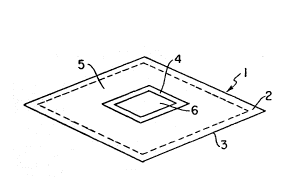
Referring to Figure 1, a composite E~I shield is shown
a~Eter molding. For illustrative purposes, the shield 1 is
essentially flat and square, requiring a clean, highly conduc-
tive edgs surface 2 (in phantom) on one si~e 3, and a clean,highly conductive edge surface 4 on the other side 5 around a
cutout area 6. Such highly conductive edge surfaces may be
obtained as taught by U.S. Patent No. 4,746,389 to DiGeno~a,
co~monly assigned herewith and hereby incorporated by
reference, which discloses a method for providing a clean,
highly conductive mating surface in a composite article.
Referring to Figure 2, an exploded view o~ the ~hield
o~ Fig. 1 i~ shown. A nonporous tape 7 is laid onto a tool or
mold surface 8 (not shown) in the edge are~ 2 required for
conductive bonding. For purposes of this disclosure, ~bonding~
means connecting various structures so that these structures
form a continuou~ electrical unit, pr~vent~ng buildup o~
electricity on one structure by discharging to the other
structures. For illustrative purposes, the tape 7 is CH0-MASK,
-tape made by the Chomerics Company, which includes a conductive
adhesive backing on a copper foil with a Mylar facing. A
nonporouC tape i~ reguired to prevent resin infiltration.
While CHO-MASX, taps i~ discussed, any nonporous material which
would SurViVQ fabrication and b~ removable from the completed
article could be used.
The tape 7 forms the periphery of the shield, and a
single compo~ite face ply 9 is then laid within the area
; de~ned by th~ tape. The ply ha~ a cutout area 10, ~or example
for u~ a~ an access hola through the shield. A rein~orcin~
ply 11, of a ~i~e to support the desired conductive edge 4 o~
the cutout area is then added. A barrier tape 12 is then laid
over thi~ reinforcing ply. A mstal mesh ply 13 i3 then laid
over the tape 7, face ply 9, and barrier 12, with the metal
mesh possibly being of an expanded aluminum foil or wire
variety. For example, an aluminum wire mesh formed from 0.0021
inch diameter wire, composed of 5056-0 aluminum and weaved at a
wire density o~ 200 wires per inch may bo used. Another metal
;
X01~7~;~
mesh ply may be laid over the first mesh ply 13. The number of
metal mesh plies employed will depend upon the degree of
shielding required for the particular application. While two
metal mesh plies are preferred, any number o metal mesh plies
may be used. The metal mesh ply is sized to cover the tape and
the barrier ply, and may include cutout areas for openings. Of
course, these could be trimmed after fabrication.
After the metal mesh is installed, a barrier taps 14 is
included above the nonporou~ taps 7 on the periphery, sandwich-
ing the metal mesh between the tapes. A composite face ply 15
is placed over the periphery of the tape 7, the ply 15 having a
cutout area 1~, into which a nonporous tape 17 is placed.
The barrier tapes prevent direct resin inclusion into
the metal mesh. For illustrative purpoqe~, the barrier tape
comprises a low flow film adhesive (AF126-2) purchased ~rom the
3M Company, which ~erves as an effective resin barrler while
providing a good internal ~ond withln the laminat~. While a
film adhesive is disclosod, any barrier material which would
prevent direct ~esin inclusion and be compatible with the
re~in/fiber combination and molding proCQSS may bq used. For
examplQ, a Mylar tape, w$th or without an adhesive peel ply
backing could be used.
Tho face or reinforcing plies may comprise resin
preimpregnated fiberglass, Kevlar~ (polyaramid), graphite or
other hybrid la~inates. After stacking, the assembly is vacuum
bagged, placed in tho appropriate autoclaving devics, heated `~
under pressure and cured.
~ During the cure cycle, resin from the composita plies
flows betweon tho plie~ to ensuie consolidation into a single
shiold. As described in U.S. Patent No. 4,746,~89 to DiGenova,
previou~ly incorporated by r~ference, the ~arrier tape prevents
th~ re~in flow from directly infiltrating the metal mesh along
the mating surfaces. However, the barrier tape does allow
indirect resin flow along the ply edges to prevent ply shift-
ing. After curing, the articlo is removed from the mold and
the edges trimmed by cutting through the barrier tape, metal
mesh and nonporous tape. Similarly, the cutout edges may be
:
~o~
trimmed. The CH0-MASK tape is then peeled off, top and bottom,
revealing two clean mesh edges suita~le for conductive ~oining
to ad~acent structures. In the case o~ exposed aluminum m~sh,
alodining may be performed to provide corrosion protection to
the mating surface while still permitting electrical conduc-
tivity. The article may then be mated to thq adjoining article
usin~ metal straps, bolts or conductive gaskets to assure a
continuously conductive joint. Fig. 3 illustrates an alterna-
tive shield in partial cross section, including additional
reinforcing plies lla, around the periphery.
It will be understood by those skilled in the art that
thQ present lnvention is not limited to the embodiments shown
and that any prepreg layup or filament wound composite struc-
ture utilizing metal mesh for EMI/lightning protection and
requiring electrical bonding to an adjoining article could
utilize this invention. In addition, the present invention is
contemplated to have application in many area~ due to the wide
usage o~ electronic devices subject to EMI, including but not
limited to automotive and household uses which require electri-
cal bonding o~ composite structures.
While this invention has been shown and described inrelation to a method of EMI/lightning shielding of aircraft, it
will b~ understood by those skilled in ths art that any other
applications requirin~ electromagn~tic shielding may utilize
the present invention. In addition, while a conductive mating
surface haQ been discus~ed, it will be understood that any
shape conductive mating ~ur~ace may be provided by simply
tailoring the barrier and nonporous tapes. For example,
square, round or oblong shapes may be produced. In addition,
the ~hap~ oS th~ shield may be molded to accommodate reces~ed
fixtures, access plates, or other structures, ~imply by
ad~usting the typa of mold surtace. Thus, complex shapes may
be constructed suitable for housing individual deviceQ of
particular sensitivity to EMI.
I clai~: