Note: Descriptions are shown in the official language in which they were submitted.
2 ~ 3
PRESS~RE-SENSITIVE MAT-FORM ELECTRIC SWI'.rCHlNG ELEMENT
FIELD OF THE INVENTION
.-.. . .
This invention refers to a pressure-sensitive mat-form
electric switching element comprising a flat electrode and a
flexible movable electrode formed by a grid of conducting
.wires, which flexible electrode can be brought in contact with
said flat electrode by applying pressure against an elastic
resetting force.
':~
BACKGROUND OF THE INV~NTION
' '
A kno~n ~witching element of this kind is disclosed in US ~.
Patent No. 4,524,256. It comprises, as a movable electrode, a
contact-mesh, said contact-mesh consisting exclusively of me-
tallic wires which extend ondulated in both weaving directions. :~
~his contact-mesh is embedded in an elastic insulating layer
: ' ,
which rises above the bare wave crests, thereby keeping them in : ~:
distance of an adjacent ~lat electrode. Upon compressing said . .
insulating layer the wave crests of the wires are moved to the
:
:
'~' '. '
! :
~ - 2 -
2 ~ 3
surface of the insulating layer, thereby contacting said flat
electrode. As soon as the compression is stopped, the resetting
forces of the elastlc insulating layer make the contact-mesh to
move into its original position in distance of the flat elec-
trode.
Manufacture of this switching element is relatively expen-
sive. A foamed material is used as the insulating layer. After ~-
embedding the contact-mesh, the insulating material is to be
mechanically removed down to the surface of the fabric. There- ~
after, the insulating material is foamed by heat-treatment in ;
order to uncover the wave crests and to increase the effective
thickness of the insulating layer as compared with the fabric
thickness, A further disadvan~age of the insulating layer is
that its elasticity may decrease due to aging, thereby altering
the pressure-sensitivity and imparing the function of the
switching element.
Another switching element, fundamentally based on the same
principles, is described in the publication DE-Al-34 24 060.
The wires of the contact-mesh are provided with an insulating
layer which i9 to be removed at the wave crests. For this, a
chemical process is proposed which is to be applied after the
mechanical removal of the elastic insulating material. By this
additional process step the~manufacturing expenses are further ~ -
increased~ ~
:
-~
, :. .
: .
:
,:
- 3 - ~ 7~
SUMMARY OF THE INV33NTION
An object of the present invention is to eliminate the dis-
advantages of the prior art described above, and to provide an
electric switching element of the kind describ~ed above which ;~
can be produced at a lower price.
In order to accomplish this object, according to the pre-
sent invention, the movable electrode of the switching element
consists of a flexible compressible contact-mesh comprising
conducting and non-conducting wires and lying on said flat
electrode. The conducting wires extend in the first direction
of weaving and are arranged essentially straight-lined in a
plane. on the other hand, said non-conducting wires, which ex-
tend in the other direction of weaving, are bent around said
conducting wires, thereby keeping said conductiny wires at some
distance rom a flat electrode contacting said contact-mesh.
When said contact-mesh is compressed said conducting wires are ;
flexibly deformed, whereby the wave crests formed on said con-
ducting wires are reaching the surface of said contact-mesh and
are contaçting there said flat electrode.
;'' '
With this solution, the conducting wires themselves take
the function of resetting, due to their bending elasticity. By
a suitable choice of the wire material and, if necessary, by
artificially aging said contact-mesh, a switching element hav-
ing highly stable switching properties can be produced.
. ..:
.:
' ' '' '
:
- 4 - ~ 6 3
Due to the absence of additional spreaders, a simple struc- ;
ture and a flat construction is achieved.
~. -
The wire gauge, which controls the thickness o~ said con- '
tact-mesh, first of all depends on the desired actuation pres-
sure of the switching element Contact-meshes according to the
invention can be woven from wires of a wide gauge range, so
that switching elements can be manufactured, both for high ac-
tuation pressures, e.g. mats or sills which may be walked on or
driven on, and for extremely low actuation pressures, e.g. con-
tact keys or contact keybords. In particular, the invention
allows to manufacture pressure-sensitive mat-form electric
switching elements the thickness of which is as low as a few~;
tenths of a millimeter.
The switching poles may be formed by two flat electrodes
. ~
which upon application of pressure~are bridged by a contactmesh ,~
arranged between themO In another embodiment, the contact-mesh
itself may be one of the switching poles which cooperates with
only one ~lat electrode, said flat electrode being arranged
either on the pressurized side of said contact-mesh, or on the
opposite slde. Alternatively, said contact-mesh may cooperate
With a plura~lity of flat electrodes arranged on the same side
of it. This arrangement ~rovides a switching element with se-
ve;ral~switching functlons, which e.g. is suitable for electric
keybords.
- - s
2 ~
In a preferred embodiment of the switching element accord-
ing to the invention, the contact-mesh lies on a stable pad and
is covered by a flexible covering coating which transfers the
pressure applied from outside to said contact-mesh and protects
the latter against disturbing influences coming from outside.
Said flexible covering coating may be e.g. a foil made of an
electrically non-conducting plastic material.
If necessary, said foil may by laminated, on the side di- -
rected towards the contact-mesh, with a contact metal, e 9.
copper. Additionally, a fine-meshed, electrically conducting
protecting fabric may be laminated into said plastic foiL for
being kept at a fixed potential in order to protect any con-
tacting elements and contacting arrangements situated below
said covering coa~ing against the influence of electric or
electromagnetic interfering radiation
The stable pad may consist of, or may comprise, at least
one flat electrode, as well.
Preferably, the conducting wires of said contact-mesh are
made of metal, e.g. copper, and the non-conducting wires are
made of plastic, e.g. a polyester. Alternatively, the metallic
wir0s may consist of a center material of very high bending
elasticity which is covered by a contact material.
In order to keep the bending stress of the electrically
".. '
6 -
' ;','
conducting wires within the region of elasticity, the ratio of
the aperture width of said contact-mesh bears to the mean dia-
meters of the conducting and non-conducting wires, which mean
diameters are almost the same, should preferab]y be fro~ about
3:1 to about 8~
The actuation pressure of the switching element can by in-
fluenced by rolling the contact-mesh. By such an after-treat-
ment, the actuation pressure may be risen or lowered, depending ;
on the wire gauge and aperture width. At the same time, rolling
provokes an artificial aging of said contact-mesh as it en-
larges the bearing surfaces at the crossing points of said con-
ducting and non-conducting wires. ThiS results in more stable
. ;. . .
switching propertie~ of the ~witching element. Al~ernatively,
artiflclal aging can be carried out by heat-treatment, or it
may be convenient to use simultaneous rolling and heat~treat-
ment.
.:
BRIEF DESCRIPTION OF THE DRAWINGS ;
''' '
FIG. 1 is a sectional view of the fundamental structure of ;
a contact-mesh according to the present invention, in combina-
tion with a flat electrode;
~ '
FIG. 2 is a top view of the contact-mesh of FIG. l; ;
,~ ~ "
FIG. 3 lS a sectional view of the structure of FIG. 1 under
; ~.
:: :
. .
:
, '
_ 7 - 2~ 3
the action of pressure;
FIG . 4 is a sectional view of a first embodiment of a
switching element according to the invention; and
FIG 5 is a sectional view of a second embodiment of a
switching element according to the invention. ;
.
PREFERRED EMBODIMENTS OF THE INVENTION : .
Now, two preferred embodiment of the present invention will `
be described with re$erence to the drawings.
The movable electrode of the electric switching element is
a flexible contact-mesh 1 comprising electrically conductlng
wires 2, extending in the first dire~ction of weaving, and elec- -
~. .- .. .
trically non-conducting wires 3, extending in the other direc- ~
.
tion of weaving. Said electrically conducting wires 2, of dia-
meter d, are arranged essentially straight-lined in a plane,
whereas said electrically non-conducting wires 3/ of diameter
D, are bent around said conducting wires 2 and are keeping them
at some distance from said flat electrode 4. With this kind of
weaving, the thickness of said contact-mesh 1 is 2D~d 5FIG. 3).
:
The aperture width m (FIG. 2) is chosen so as to give ratio
d/m, or D/m respectively, of 3:1. In manufacturing th1s con-
tact-mesh, it is convenient t~o make the straight-lined wires 2
,
::
~ - 8 - 2Q~7~
the weft and the intensely bent wires 3 the wrap of the fabric.
'. "
When a pressure is created by applying a force P, the con-
ducting wires 2 are ondulated by the non-conducting wires 3, as
. .
shown in FIG. 3. The wave crests formed on saidl conducting ,
wires 2 are reaching the surface of said contact-mesh and are
contacting there said flat electrode 4. In the area of pres-
sure, the th1ckness of said contact-mesh 1 is reduced from 2D+d -;
to D+d. A flexible covering coating 5 transfers the pressure
applied from outside to said contact-mesh 1 thereby protecting
said flexible contact-mesh 1 against disturbing influences com-
ing from outside, such as dust and humidity.
"' `
Preferably, the thickness of the Elexible covering coating
5 i9 chosen 50 as to distribute the pressure on a plurality of
meshes, thereby creating an area o~ pressure which at all
events is larger than shown in the schematic view of FIG. 3.
The diameters d and D of the wires and the aperture width m
are chosen in a manner that the excursion o~ said conducting
wires 2, upon execution of the switchin~ operation, is kept
within the region of elasticity, so that said conducting wires
2 take again their distance from said flat electrode 4 and
their original elongated form when the pressure is released.
: .
Tects carried out on practical embo~iments showed that a
flexible contact-mesh consisting o~ a copper wire of a diameter
, ~ .
,
.
: ~ ~` '. '
,- -
' .
6 3
~ _ 9 _
d of 0022 mm and a polyester wire of a diameter D of 0.16 mmand having an aperture width m of 3:1 provides a switching ele-
ment, the actuation pressure of which is 2.5 to 3.0 MPa ~25 to
30 kg/cm2 ) . By reducing the diameter of the copper wire to
0.112 mm, without change of the other parameters, the actuation
pressure may be reduced to 0.8 MPa (8 kg/cm2).
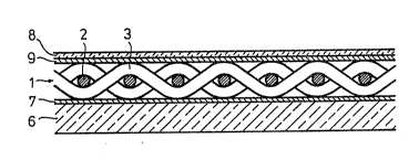
The switching element of FIG. 4 comprises a contact-mesh 1
of the kind described with reference to FIGSc 1 to 3~ Said con-
tact-mesh 1 lies on a stable pad 6 of insulating material which
comprises a flat electrode consisting of a metallic coating.
The covering coating is a foil 8 of insulating material, pro-
vided wlth a metallic coating 9 as well. Both said metallic
coatings 7 and 9 face the flexible contact-mesh 1, and are con-
nected to each other by said conducting wires 2 when the con-
tact-mesh is compressed as shown in FIG. 3.
'
Alternatively, said conducting wlres 2 may be connected to
each other e.g. at the edge of the fabric, thereby jointly
forming a switching pole. In this case, one of the metallic
coatings 7 and 9, this is to say one of the flat electrodes,
may be omitted.
.
The switching element shown in FIG. 3 comprises the same -~
.
type of contact-mesh 1 and a stable pad 10 o insulating mate~
rial as well. Several flat electrodes 11 (two of which are
:
shown in the drawing) which are connected to separate conduc-
' .
'
,,::
. . .
.
' . ': .
..
o 2 ~
;
tors 12 are provided for on said stable pad 10. The movable :
electrode is common to all flat electrodes 11 since all con- .
ducting wires 2 of said contact-mesh 1 are interconnected ~not
shown). The movable electrode may alternatively be contacted :-
with one of the flat electrodes 11 by locally aLnd selectively
applying pressure so as to limit the area of pressure to the
area of one of the flat electrodes 11. The covering coating is
a plastic laminate 13 which is laminated into a fine-meshed
protectlng screen 14 consisting of metal.
. .
.
" .: '
',' "
:
.:
,;-...