Note: Descriptions are shown in the official language in which they were submitted.
` 2~1718~
The invention relates to a method of making a
variable capacitor microphone and to a microphone made by the
method.
Capacitor microphone6 in which a permanently polar-
ized dielectric, or electret, is used to obviate the need for
an external high-voltage supply are well known in the art.
Because of their small size, relative insensitivity to tem-
perature or humidity changes, and extended high-frequency re-
sponse, they are especially suited for use in citizen's-band
transceivers, military communications systems and the like.
one such electric microphone is shown in Cote U.S. Patent No.
4,443,666, owned by the assignee herein.
In the microphone shown in the above-identified
patent, an insulating substrate carries a metal electrode
which in turn supports an electret. The electret comprises a
fluorocarbon polymer such as the one sold by E. I. du Pont de
Nemours and Company under the trademark TEFLON. A diaphragm
comprising a metallized polyester such as the one sold under
the trademark MYLAR, disposed at a spacing from the electret,
serves as a second electrode. Vibration of the second elec-
trode in response to acoustic vibrations gives rise to a
corresponding variation in the instantaneous displacement
between the two electrodes, producing in turn a momentary
variation in the potential difference between the two elec-
trodes. This potential variation is applied to the gate of a
field-effect transistor (FET) carried on the other side of
--1--
,
.
. .
. . . ~, . , : :
2~1718~
the substrate, which in turn is coupled to an exten~al ampli-
fication system.
In the fabrication process conventionally used,
individual electrets of the desired shape are cut from a
previously polarized sheet of TEFLON or other fluorocarbon
polymer and bonded to the electrode carried by the substrate,
following which the other elements of the electret microphone
are assembled. It has been found that electrets made by this
conventional process tend to discharge after a relatively
short period of time, especially in moist environments.
While the exact explanation of this premature discharge is
not known, it is believed that the repeated handling of the
electret following its initial formation is a contributing
factor.
Another problem experienced with this conventional
fabrication process is the tendency of the electret not to
adhere to the electrode to which it is applied.
Still another problem experienced with the conven-
tional fabrication process involves the polarization of the
dielectric layer. One common method of polarizing the di-
electric entails the use of a corona to ionize a gaseous
region ad~acent to the layer to generate charged particles.
Although coronas generate the desired charged particles, they
also undesirably generate ozone.
--2--
....i .
.
.
: , .- : : .: : :.
.. ~. .: ,, . , :
,,.
: : . : ~.. .. .
2~17~8~
SUMMARY OF THE INVENTION
One of the features of our invention is to provide a
method of making a variable capacitor microphone comprisinq
an electret that maintains its polarization after a long
period of time, even in moist environments.
Another feature of our invention is to provide a
variable capacitor microphone comprising an electret that
satisfactorily adheres to a substrate to which it is applied.
Our invention contemplates a method of making a
variable capacitor microphone in which the fixed capacitor
element is formed by first coating the metallized surface of
a relatively rigid insulating substrate with a polarizable
dielectric material which preferably is a fluorocarbon and
more particularly a fluorinated ethylene-propylene copolymer
such as the one sold under the trademark TEFLON.
The coating is preferably applied to a plurality of
conductive supports carried by a single substrate, preferably
by spraying through a mask. Next, the dielectric carried by
the substrate is permanently polarized. More particularly, a
pair of electrodes, one of which preferably supports the
substrate carrying the dielectric and is heated, define a
region therebetween capable of containing an ionizable gas
such as air. The region i8 exposed to alpha radiation to
generate charged particles of a given polarity from the gas,
and a potential i5 applied to the electrodes to effect
electrostatic deposltion of the particles on a dielectric
disposed in the region. Preferably, the alpha radiation
source, which may comprise polonium 210 as noted above, is
rn/~p
.. . .
:' .. : ':.
- :: ~
2~1718S
disposed relatively adjacent to the charging electrode and is
shielded from the heating source.
We have found that by using an alpha source such as
polonium 210 as an ion generator, we can effectively polarize
dielectrics to form electrets. At the same time, by avoiding
the use of a corona generator with its attendant high-
intensity field, we avoid the undesirable result of
generating ozone.
We have found that by forming the dielectric layer
in situ in the manner described above on the surface of the
conductive support, we ensure satisfactory adhesion between
the dielectric and the support. Further, since the
dielectric layer is polarized only after it has been formed
on the conductive support, subsequent handling of the
dielectric, which may result in charge dissipation, is
minimized. After the insulating substrates carrying the
electret to form six capacitor elements have been formed in
the manner described, they are mounted in spaced relationship
to flexible diaphragms to form the variable capacitor
microphones.
rn/5p
: :' . ''
, . ~
.. .
' .'~ ~:.' : ' '
~1718~ -
Brief Description o~ the prawings
In the accompanying drawings to which reference is
made in the instant specification and which are to be read in
conjunction therewith and in which like reference numerals
are used to indicate like parts in the various views:
PIGURE 1 is a section along line 1-1 of FIGURE 2 of
a microphone incorporating an electret constructed in accord-
ance with our invention.
FIGURE 2 is a section of the electret microphone of
FI~URE 1 along line 2-2 thereof.
FIGURE 3 is a top plan of the circuit board of the
microphone shown in FIGURE 1 as it looks before the electret
is formed thereon.
FIGURE 4 is a schematic diagram of the electret
microphone of FIGURE 1 and the preamplifier circuit associat-
ed therewith.
FIGURE 5 is a top plan of the substrate from which
the individual circuit boards are formed.
FIGURE 6 is an enlarged fragmentary top plan of the
upper left portion of the substrate shown in FIGURE 5.
FIGURE 7 is a top plan of the mas~ used while
spraying the dielectric onto the substrate shown in ~IGURE 5.
FIGURE 8 is a section showing the spraying of the
dielectric onto the sur~ace of the substrate.
FIGURE 9 is a partly schematic side elevation of
the apparatus used ~or permanently polarizing the dielectric
~ormed by the spraying process as shown in FIGURE 8.
,~ -5-
' , '; '
2017185
FIGURE 10 i~ a partly schematic fragmentary en-
¦ larged side elevation of the apparatus shown in FIGURE 9.
n~scription Of The Preferred Embodiment
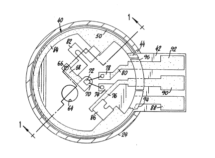
¦ Referring to FIGURES 1 to 4, a microphone 20 incor- .
¦ porating an electret constructed in accordance with our
¦ invention includes a conductive base or lower housing portion
22 and a conductive cap or upper housing portion 24 which
¦ fits over the base 22 in intimate sliding contact therewith
¦ as shown in FIGVRE 1 to form a conductive housing. cap 24 is
¦ formed with a port 26 and with a larger-diameter recess 28 on
¦ the outer side of the port for receiving a wire screen 30.
¦ Likewise, base 22 is formed with a port 32 and with a larger-
¦ diameter recess 34 on the outer side of the port for receiv-
. ¦ ing a,wire screen 36. If desired, the inner side of port 32
¦ may be fitted with an acoustically transparent shield 3~ to
¦ protect the components to be described from moisture. A
¦ circuit board 40 includes a circular portion, supported by
the upper rim of base 22 inside the housing, and a rectan-
¦ gular exposed portion or tab 42, which extends out of the
l housing through a slot 44 formed in the sidewall of cap 24.
A nonconductive outer epoxy seal 46 extends along the lower
¦ edge of cap 24 and along the interface between tab 42 andba8e 22. Preferably, base 22 iB formed with an indentation , ¦
l 48 around its lower periphery to accommodate the epoxy seal
2~ 1 46.
Circuit board 40, which supports the transducer and
eleotronlc elements of the microphone 20, is formed from an .
lnsulatlng aeramic support 50 having a circular palladium-
8ilver electrode 52 formed on the upper,surface of the en-
- , ' ,
20~71~
closed portion of the board, as shown in FIGURE 3. A per-
manently polarized disk-shaped electret 54 (not shown in
FIGURE 3) is formed on the upper surface of the electrode 52
in accordance with our invention, as described below. A
concentric palladium-silver support ring 56 surrounding
electrode 52 on the upper surface of the board 40 supports
the periphery of the electret s4. Electret 54 in turn sup-
ports an annular spacer 58, preferably comprising a polyester
material such as the one sold under the trademark MYLAR.
Spacer 58 in turn has bonded thereto a diaphragm 60 also
comprising a polyester such as MYLAR and having a gold plat-
ing (not separately shown) on its upper surface as viewed in
FIGURE 1. Electrode 52, electret 54, spacer 58 and diaphragm
60 together constitute the transducer portion of the micro-
phone 20. An annual shoulder 62 formed on the inner surface
of cap 24 presses the diaphragm 60 and spacer 58 against
electret 54 and support ring 56 to sandwich the board 40
between the upper rim of base 22 and spacer 58.
Board 40 is formed with a first, relatively large-
dlameter bore 64 to form an acoustic coupling between the two ,
slde~ of the board. In addition, board 40 is formed with a
smaller-diameter bore 66, which is plated through with pal-
ladium-silver to provide an electrical coupling between elec-
trode 52 and a palladium-silver plsted area 68 on the lower , ¦
~ide of board 40 ad~oining a gold plated area 70. Plated
sreA 70 i~ connected to the gate electrode o~ a ~ield-effect
tr~nsi~tor ~FET) 72 carrled on the lower sur~ace o~ board 40.
FET 72 has its ~ource electrode coupled to a gold plated area
74 ad~olning a palladium-silver plated area 76 and has its
draln eleatrode coupled to a gold plated area 78 adjoining a
: ~ . , . ., .................. -. . :............ . . .
~' . . , :
2~71~5
palladium-silver plated area ~0 also formed on the lower
surface of board 40. A gate resistor 82 provides a conduc-
tive path between plated area 68 and a peripheral palladium-
silver plated area 8~ formed on the lower surface of board
40, while a 60urce resistor 86 couples plated area 76 to the
same peripheral area 84.
A first electrical terminal or contact 88 formed on
the lower surface of tab 42 extends inwardly through slot 44
to join plated area 84. A second electrical terminal 90
formed on the lower surface of tab 42 extends through slot 44 !
to join plated area 76, while a third terminal 92 formed on
the lower surface of tab 42 extends inwardly through slot 44
to join plated area 80. Preferably, terminals 88, 90 and 92
are formed of the same material as the plated areas that they
~oin. A conductive epoxy layer 94 generally coextensive with ¦
annular plated area 84 couples area 84 electrically to base
22 and hence ca~p 24 to allow area 84 to serve as a ground or
common line. Terminal 92 provides an external connection to
the common plated area 84, while terminals 90 and 92 provide
external connections to the source and drain, respectively, I
of FE~ 72, as shown in FIGURE 4. A nonconductive epoxy layer ¦
96 6eparstes the inwardly extending portions o~ terminals 90
and 92 from the upper rim of base 22 to preclude the pos-
sibillty of a short circuit.
Sultable values for the mechanical dimensions,
electrical parameter6 and the like will be apparent to those
~killed ln the art. Satis~actory results have been obtained
With the following choice6:
20:~7 ~
Substrate (50) thickness 0.020 inch
Substrate (50) diameter 0.285 inch
Tab (42) width 0.148 inch
Tab (42) length 0.125 inch
Electrode (52) diameter 0.200 inch
Ring (56) ID 0.225 inch
Ring (56) OD 0.275 inch
Acoustic bore (64) diameter 0.041 inch
Electric bore (66) diameter 0.010 inch
Plating thickness 0.0005 inch
Diaphragm (60) thickness 0.00025 inch
Spacer (58) thickness 0.002-0.003 inch
Source resistor (86) 4.7-10 kn
Gate resistor (82) 1000 Mn
FET t72) 2N4338
Screen (30, 36) mesh size 5 ~m
Referring now to FIGURES 5 and 6, a plurality of
circuit boards 40 are formed from a single wafer 100, in
which the circular portions of the boards and the sides of
the tabs 42 are defined by laser cuts 102. The individual
boards 40 are 50 arranged on the wa~er 100 that the ends of
the tabs 42 lie along lines 104 defined by scribes formed on
the lower sur~ace o~ the wafer 100. ~ypically, wafer 100 may
be about 2.5 lnche~ square and contain 33 in~ividual boards
40.
To form circuit boards 40 containing electrets 54,
a ceramic wafer 100 i3 first drilled to form the bores 64 and
66 of the indivldual boards, and ~ormed with laser cuts 102
_g_
~o~lo~
and scribe lines 104 to permit the individual boards 40 to be
¦ snapped away from the remainder of the wafer along the scribe
lines. The upper and lower surfaces of the individual boards
l 40 on the wafer 100 are then plated witll areas of palladium-
~ silver and gold, as described above. After this platingl step, gate resistor 82 and source resistor 86 are screened
! onto the lower surfaces of the boards, as shown in FIGURE 2~
Next, the TEFLON fluorocarbon dielectric is applied
ll to the front surface of each of the individual circuit boards
¦ 40 by using an applicator 110 to spray the upper surface of
¦ the wafer 100 through a mask 106. As shown in FIGURES 7 and
¦ 8, mask 106, which rests on the surface of the wafer 100
during spraying, comprises a flat metal (e.g., brass) stencil
! formed with a plurality of apertures 108 concentric with and
¦ corresponding in diameter to the outside diameter of rings
56. Apertures 106 may be formed by any suitable process such
as chemical etching. Preferably, DuPont 856-200 TEFLON FEP
clear coating, an aqueous solution of FEP (fluorinated ethyl-
l ene-propylene copolymer) having a viscosity of 25-300 cen-
l tipoise (cP), is used. Preferably, no primer is used, and
the solution not diluted. Before being applied, the material
is preferably gently agitated at room temperature by rolling
its container Sor 15 to 30 minutes, and then filtered through
a 100 mesh stainles~ steel screen. Applicator 110 may com-
prise a standard compres6ed-air spray gun of the type used
in painting. One suitable spray gun is a DeVilbiss Model
M~C, operating at a pressure oS 40 psi, with a ~30 air cap
with an F tip. The thickness oS the applied dielectric layer
5q ls controlled by the number oS coatin~s. Preferably, no
more than 1 mil of coating i8 Sormed per application.
2017i8a
After each coat of dielectric is applied in this
manner to the front surface of wafer 100, it is thermally
cured in accordance with the manufacturer's specifications to
evaporate the solvent. Satisfactory results have been ob-
tained with a total coating thickness of 1.5 mils, each coat
being baked ~or 1 hour at 700~F. After the desired number of
layers of dielectric have been applied in this manner, FETs
72 are applied to the lower surfaces of the individual boards
40, their leads bonded to gold-plated areas 70, 74 and 78,
and the FETs potted over with epoxy (not shown). The in-
dividual boards are then separated from the wafer, as a
preliminary to the charging step to be described below, by
snapping them off at the ends of the tabs 42 along scribe
¦ lines 104.
I Referring now to FIGURES g and 10, the charging
¦ apparatus, indicated generally by the reference numeral 112,
¦ includes a conductive support 114, the upper surface of which
! i6 formed with a well 116 for receiving an individual circuit
¦ board 40 with the lower surface thereof face down. As shown
I in FIGURE 10, well 116 is formed with a further recess 11~ to
¦ accommodate the electronic components on the lower surface of
the board 40. Support 114 rests on a brass workstation 120,
which in turn has a conductive base 122. A resistive element
l 124 disposed within workstation 120 is adapted to be coupled
l to a source o~ potential v1 to heat the circuit board 40 to a
suitable tamperature during the charging process. A heat
shield 126 disposed between support 114 and workstation ]20
~hields the electrode to be described from heat from the
workstation 120.
11 1
~017i~5
Conductive support 114 not only supports circuit
board 40, but serves as a first electrode, to which the elec-
trode 52 supporting the electret 54 is coupled through the
l electronic components on the lower surface of the board. A
¦ chargi~g elsctrode 128 disposed at a predetermined distance d
from sùpport 114 is adapted to be coupled to a source of
highly negative potential v2 to create a potential gradient
in the region between electrode 128 and support 114. Prefer-
l ably, electrode 128 comprises a metal (e.g., brass) disk
! supported by suitable means (not shown) for pivotal movement
between an operative position (FIGURES 9 and 10) in register
with workstation 120 and support 114, with a breach or gap of
¦ width d, and an inoperative position out of register with
¦ support 114. An ion generator 130 secured to the lower sur-
¦ face o~ electrode 128 ionizes the air in the region adjacent¦ electrode 128, generating charged particles including posi-
¦ tive ions 132, negative ions 134 and electrons 136. Prefer-
¦ ably, ion generator 130 comprises an alpha emitter such as
¦ polonium 210, which is a short-range, short-life material.
l Since, as described above, the electrode 128 is
maintained at a highly negative potential relative to support
l 114, positive ions 132 formed in the gap are attracted to
¦ electrode 128, while negative ions 134 and electrons 136 are
l attracted toward the support 114 and hence dielectric layer
l 54. Those electrons and negative ions that reach the dielec-
tric 54 without recombining with positive ions impinge upon
the surface Oe the dielectric layer 5~. Owing to thermal
activlty in the dielectric layer 5~, those electrons and
l negatlve ions are absorbed onto or into the material, produc-
¦ ing a layer Oe a negative charge (not separately shown) at or !
~ -12-
. . .
2i~171~5
adjacent to the upper surface of the dielectric layer. That
charge remains when the charging electrode 128 is removed and
the dielectric layer 54 cooled.
In operation, an individual circuit board 40 on
¦ which a dielectric layer 54 has been formed is placed in the
¦ well 116 of support 114 and allowed to reach a suitable tem-
¦ perature. The electrode 12~ and ion generator 130 are then
¦ swung into position opposite the support 114 at a spacing d
I¦ therefrom. The dielectric layer 54 on board 40 is then
¦¦ charged for a predetermined time. The electrode 128 and ion
generator 130 are then removed and the board 40 quickly
cooled. To verify the charge level the board 40 is placed
under an electrostatic voltmeter (not shown). If the mea-
l sured voltage is acceptable, the board 40 is used to assemble
15 l¦ a microphone as shown in FIGURES 1 to 4.
¦ The gap width d controls the rate and thus amount
of charqe on the surface of layer 54 for a given time, tem-
perature and charging voltage v2. Suitable choices for the
charging voltage v2, temperature, time and gap width d will
be apparent to those skilled in the art. Satisfactory re-
sults have been obtained using a voltage v2 of -3000 volts,
a time of 20 seconds, a temperature of 175~C and a gap width
d of 0.5 inch.
Certain variations of the proces~ described above
will be apparent to those skilled in the art. Thus, while
heating the dielectric during the charging step is desirable,
it 18 not e6ssntial. Further, while the use of a ma6k is
deslrable to prevent the deposition o~ dielectric onto the
taba ~2 o~ the circuit boards, such a ~tep i8 likewise not
essential.
-13-
2 ~ 5
It will be seen that we have accomplished the ob-
jects of our invention. Our electret maintains its polariza-
tion after a long period of time, even in moist environments,
and satisfactorily adheres to a substrate to which it is
applied. Further, the disclosed process for making an elec-
tret does not result in the generation of ozone.
It will be understood that certain features and
¦subcombinations are of utility and may be employed without
reference to other features and combinations. This is con-
templated by and within the scope of our claims. It is fur-
ther obvious that various changes may be made in details
¦ within the scope of our claims without departing from the
¦ spirit of our invention. It is, therefore, to be understood
that our invention is not to be limited to the specific de-
1 tails shown and described.
l~aving thus described our invention, what we claim
is:
-14-