Note: Descriptions are shown in the official language in which they were submitted.
~; TN-7827
- - - 1 2~1728~`
OPTICAL RECORDING MEDIUM
BACKGROUND OF THE INVENTION
1. Field of the Invention
The present invention relates to an optical
recording medium in which information is recorded,
reproduced and erased by a light such as a laser beam.
More specifically, the present invention relates to an
optical recording medium having a metal reflecting
layer, and is particularly preferably applicable to a
magneto-optical recording type optical recording medium.
2. Description of the Related Art
Optical recording media are now being
investigated and developed because of their ability to
provide a high density recording and their large
- capacity for storing information. Particularly, a
magneto-optical recording medium is required, and
various materials and systems have been proposed
because of the wide applicability of these media to
various fields.
Many magneto-optical recording materials
including, for example, TbFe disclosed in Japanese
unexamined Patent Publication (Kokai) No. 52-31703,
TbFeGd disclosed in Japanese Unexamined Patent
Publication (Kokai) No. 56-126907, TbFeCo and DyFeCo
disclosed in Japanese Unexamined Patent Publication
(Kokai) No. 58-73746, and NdFe disclosed in Japanese
Unexamined Patent Publication (Kokai) No. 61-165846,
have been proposed. Nevertheless, a further improvement
of the recording and reproducing characteristics of the
media using these materials must be made be~ore these
media can be practically used.
Accordingly, a metal reflecting layer formed
on a magneto-optical recording layer or that formed on a
dielectric layer present on a magneto-optical recording
layer has been proposed, and this is advantageous
because a high carrier to noise ratio (C/N ratio) is
~ - 2 - 2Q17284
obtained by utilizing the Faraday effect as well as the
Kerr effect. As such a metal reflecting layer,
proposals including, for example, a layer of Al
disclosed in Japanese Unexamined Patent Publication
(Kokai) Nos. 58-83346 and 59-132434, a layer of Cu
disclosed in Japanese Unexamined Patent Publication
(Kokai) No. 59-8150, a layer of an Al-based alloy
disclosed in Japanese Unexamined Patent Publication
(Kokai) No. 62-137743, a layer of stainless steel
disclosed in Japanese Unexamined Patent Publication
(Kokai) No. 59-171054, a layer of Te disclosed in
Japanese Unexamined Patent Publication (Kokai)
No. 62-52744, and a layer of an amorphous metal
disclosed in Japanese Unexamined Patent Publication
(Kokai) No. 59-171054, have been made. Nevertheless,
when a layer of a metal having a high reflectivity such
as Ag, Al, Cu or the like is used, the recording
sensitivity is remarkably lowered because of a high
thermal conductivity thereof, and when a layer of a
metal having a relatively low thermal conductivity such
as Te, stainless steel or the like is used, the
recording sensitivity is increased but a sufficiently
high C/N ratio is not obtained because of a low
reflectivity thereof.
Moreover, a recording layer tends to
deteriorate under high temperature and high humidity
atmospheric conditions, and therefore, the recording
layer must be protected by the metal layer.
To solve the above problems, an addition of Ta
to Al is proposed in Japanese Unexamined Patent
Publication (Kokai) No. 64-4938, an addition of Ti, Mg
or a transition metal to Au, Ag, Al or Cu is proposed in
Japanese Unexamined Patent Publication (Kokai)
No. 59-38781, an addition of Cu-Mg, Mg-Si, Cr, Sn, or Mg
to Al is proposed in Japanese Unexamined Patent
Publication (Kokai) No. 62-239349, and an addition of Ti
to Al is proposed in Japanese Unexamined Patent
.~
20 i 72&4
_ -- 3
Publication tKokai) Nos. 62-137743 and 64-66847. These
alloy layers bring an improvement of the thermal
conductivity to some extent, while maintaining a high
reflectivity thereof. Nevertheless, a considerable
amount of the additive metal(s) is needed in the above
alloys, to improve the durability of the medium under
high temperature and high humidity conditions, and thus
lowers the reflectivity below the level necessary for a
reflecting layer. Accordingly, the above alloy
reflecting layers cannot satisfy the requirements for
both the reflecting layer and the protecting layer.
Furthermore, in the case of an Al alloy, a
problem arises in that a uniform target of the alloy for
sputtering is difficult to obtain, but such a uniform
target is essential for commercially producing media
using the Al alloy reflecting layer. Namely, a large
difference of the melting points between Al and the
additive metal prevents the production of a uniform Al
alloy by a melting process. Namely, the melting point
of Al is 660C and those of the above additives are from
1453C of Ni to 2977C of Ta. Therefore, only a small
amount of the additive metal can be uniformly mixed in
the Al alloy, or if a larger amount of the additive
metal is mixed for an effective lowering of the thermal
conductivity of the alloy, only a non-uniform can be
obtained.
SUMMARY OF THE INVENTION
The object of the present invention is to provide
an optical recording medium having a high sensitivity, a
high C/N ratio, and a high durability, by improving the
metal reflecting layer.
The above and other objects and features of the
present invention can be attained by an optical
recording medium comprising: a transparent substrate;
an optical recording layer deposited over the substrate;
and a metal reflecting layer deposited over the
recording layer; wherein the metal reflecting layer
.~
20~72~4
_ - 4 -
consists essentially of an alloy of aluminum with 0.5 to
20 at%, preferably 2.0 to 15 at%, gold or an alloy of
silver with 0.5 to 30 at%, preferably 2.0 to 15 at%,
gold.
BRIEF DESCRIPTION OF THE DRAWINGS
Figure 1 shows the reflectivity of a metal
reflecting layer of an Al alloy with an additive in
relation to the content of the additive; and
Figures 2-6 schematically show sections of optical
recording discs.
DESCRIPTION OF THE PREFERRED EMBODIMENTS
The present inventors investigated ways in which to
overcome the above-mentioned problems, and found that a
metal reflecting layer of an alloy of Al or Ag with Au
provides an optical recording medium having a high
recording sensitivity, a high C/N ratio, and a high
durability, and an alloy of Al with Au is easily
produced in a uniform sputtering target.
Surprisingly, it was found that the thermal
conductivity of Al or Ag is lowered by alloying with Au
having a high thermal conductivity (higher than that of
Al), and that the reflectivity of the alloy remains high
although the thermal conductivity thereof is lowered by
the alloying. Figure 1 shows the reflectivity at 830 nm
of a metal reflecting layer of Al alloys of AlAu, AlTi,
AlTa or AlZr in relation to the content of the
additives. It is seen that the reflectivity of the Al
layer is generally lowered by an addition of an additive
such as Ti, Ta or Zr, and the degree of the lowering of
the reflectivity is in proportion to the added amount of
the additive. In contrast, although the thermal
conductivity is lowered by alloying with Au,
surprisingly, the reflectivity of the Al layer is
increased by an addition with Au up to a certain
content, and not lowered in proportion to the amount of
the added additive of Au.
In the case of an Al-Au alloy, it is considered
~ .
`- 201728~L
-- 5
that the above phenomenon is due to the formation of an
intermetallic compound of Al2Au. For example, in an
X-ray diffraction of a prior art Al alloy layer formed
by sputtering an Al target with chips of Ta, Zr or Ti
thereon, only diffraction peaks from the (l,l,l) plane
of the face centered cubic (fcc) crystal lattice of Al
were observed. In contrast, in an X-ray diffraction of
an Al-Au alloy layer of the present invention, the
diffraction peaks of the fcc crystal lattice of Al
disappeared and diffraction peaks of the (l,l,l) and
(2,2,0) planes with interplanar spacings 0.349 nm and
0.214 nm of the intermetallic compound Al2Au were
observed. Thus, a formation of the intermetallic
compound Al2Au was confirmed and it is considered that
this intermetallic compound Al2Au contributes to a
lowering of the thermal conductivity.
The amount of Au to be added to Al or Ag is from
0.5 to 20 at%, preferably 0.5 to 15 at% for Al, and 0.5
to 30 at%, preferably 0.5 to 15 at% for Ag. If the
amount of Au is less than 0.5 at%, little improvement of
the recording sensitivity or lowering the thermal
conductivity is obtained. If the amount of Au is higher
than 20 at% in an Al-Au alloy or higher than 30 at% in
an Ag-Au alloy, the effect of the improving the
recording sensitivity is saturated and the C/N ratio is
slightly lowered, probably due to a lowering of the
reflectivity. The durability of a medium is also
preferable in this range of the added amount. Note that
the intermetallic compound Al2Au should be present in an
adequate amount and dispersed in the Al-Au alloy layer,
and should not cover the entire layer, to obtain the
above preferable effects.
Further, it was also found that, by adding a
certain element to an alloy of Al or Ag with Au, an
improvement of the recording sensitivity or a lowering
of the thermal conductivity, an increase of the C/N
ratio, and an increase of the durability of an optical
~ .
2017284
-- 6
recording medium are obtained. The above certain
element is at least one element selected from the group
consisting of Ti, Ta, Zr and Y. By adding at least one
of these elements, the effects of an addition of Au as
mentioned before can be obtained by a lesser amount of
Au and thus the cost can be reduced. Particularly, an
Ag alloy with 0.5-15 at% Au and 0.3-12.0 at% at least
one of the above elements is preferable due to its
excellent recording sensitivity, durability under a high
temperature and high humidity, C/N ratio, and cost, and
such an Ag alloy having a total content of Au and said
certain element of 1.0-15 at% is more preferable. Also,
an Al alloy of 0.5-15 at% Au and 0.3-5.0 at% of at least
one of the above elements is preferable, since if the
content of said certain elements is more than 5.0 at%,
the reflectivity of the layer is lowered and the
formation of a uniform alloy target becomes difficult.
When the content of said certain element is up to 5.0
at%, a lowering of the reflectivity of an Al-Au alloy
layer is less than 2%, and the reflectivity of the Al-Au
alloy layer is 86-82%. The total content of Au and the
above elements is more preferably 1.0-15 at%.
Note, in an electron beam diffraction of an alloy
layer of A189Au8Ti3 having a thickness of 100 nm, a
diffraction ring of A12Au in addition to that of Al was
found. A transmission type electron microscopy of the
above alloy layer revealed that the alloy layer is
composed of a uniform assembly of very fine crystallites
having a size of a few nm to 10 nm. Similar results
were obtained in an Al-Au alloy layer. In contrast,
when an Al layer and an AlggTil alloy layer having a
thickness of 100 nm were examined in the same way,
crystallites having various sizes of 30 nm to 100 nm
were observed. Thus, the high durability of an optical
recording medium having a metal reflecting layer of an
Al-Au alloy is considered to stem from not only an
addition of the inert Au but also the dense structure of
;
20172~
-- 7
the alloy layer as shown above.
The thickness of the metal reflecting layer of the
above alloy is preferably lO to 200 nm, more preferably
30 to 80 nm. If the thickness of the layer is too
thick, the recording sensitivity is lowered, and if the
thickness of the layer is too thin, the reflectivity of
the layer is lowered and the C/N ratio is reduced.
The metal reflecting layer may be formed by a
conventional evaporation, sputtering, ion beam
sputtering, chemical vapor deposition (CVD), etc., but
sputtering is preferred because of an adhesive force
thereof to the underlaying layer, a controllability of
the composition, and a uniformity of the composition.
The deposition rate-and sputtering gas pressure, etc.
may be appropriately selected in consideration of the
productivity and the internal stress of the layer.
The optical recording medium is apparently not
particularly limited as long as a reflecting layer is
used, and may be a magneto-optical recording medium, a
compact disc, a video disc, and the like. It is
particularly applicable to a magneto-optical recording
medium bearing a rare earth metal in the recording
layer, in which the rare earth metal is sensitive to
oxidation.
The magneto-optical recording medium may have any
recording layer which utilizes the magneto-optical
effect; typically, a magnetic layer having an easy
magnetization axis perpendicular to the surface of the
recording layer and thus a high magneto-optical effect,
for example, of amorphous rare earth metal-transition
metal alloys, such as TbFe, TbFeCo, TbGdFe, NdDyFeCo,
etc. The thickness of the magneto-optical recording
layer is lS to lO0 nm, preferably 20 to 50 nm.
The layer structure of the magneto-optical
recording medium is not particularly limited except that
a metal reflecting layer is placed on a side of a
magneto-optical recording layer opposite to the light
`;.
2017~84
-- 8
incident side. A structure having a transparent
dielectric layer between the metal reflecting layer and
the magneto-optical recording layer is preferable, since
it improves the recording sensitivity, C/N ratio and
durability. In this case, the thickness of the
transparent dielectric layer should be thin, not more
than 60 nm, to obtain the desired effects. A thin
transparent dielectric layer does not allow to obtain a
sufficient thermal insulating effect, and therefore, the
metal layer of the present invention is still effective.
Nevertheless, the content of Au or other additive
element in the metal reflecting layer may be lowered
along with an increase of the thickness of the
transparent dielectric layer. A structure further
having another transparent dielectric layer between the
substrate and the magneto-optical recording layer is
more preferably because it provides a further
improvement of the C/N ratio and a prevention of
humidity permeation. On the other hand, a structure
having a metal reflecting layer in contact with the
magneto-optical recording layer also allows practically
efficient results if the metal reflecting layer is of an
Al-Au or Ag-Au alloy. This structure allows an
elimination of a transparent dielectric layer, and is
preferable from the viewpoint of productivity and cost.
These structures may be selected depending on the
purpose of a medium.
The transparent dielectric layer between the
magneto-optical recording layer and the substrate or the
metal reflecting layer should have effects such as an
enhancement of the Kerr effect, etc., and therefore,
preferably has a relatively high refractive index. The
transparent dielectric layer should be also transparent
to a laser beam to be used. As such a transparent
dielectric layer, oxides, nitrides, sulfides, carbides
or fluorides of metals or composites thereof may be
used. For example, silicon oxide, indium oxide,
';.
20~728~
g
tantalum oxide, aluminum oxide, silicon nitride,
aluminum nitride, titanium nitride, zinc sulfide,
magnesium fluoride, aluminum fluoride, silicon carbide
and composites thereof can be mentioned. These
dielectrics may have a little light absorption at a
level such that the C/N ratio is not remarkably reduced.
The transparent dielectric layer may contain a metal
element within such a tolerated amount. Further, an
organic material such as poly-para-xylylene, polyimide,
paraffin, etc. may be applied to the transparent
dielectric layer. The transparent dielectric layer may
be a composite layer or lamination of the above layers.
A transparent dielectric layer in contact with the
magneto-optical recording layer, sensitive to oxidation,
is preferably of a nitride or the like not containing
oxygen, to prevent an oxidation or deterioration of the
recording layer. Among others, silicon nitride,
aluminum nitride and aluminum silicon nitride are
preferable from the viewpoint of the layer quality and
internal stress thereof.
The optimum thickness of the transparent dielectric
layer is varied depending on the medium structure and
the refractive indices of the layers. For example, in a
structure having transparent dielectric layers on both
sides of the magneto-optical recording layer, an optimum
thickness of the transparent dielectric layer between
the magneto-optical recording layer and the metal
reflecting layer is varied by a thickness of the
transparent dielectric layer between the magneto-optical
recording layer and the substrate, and therefore, cannot
be determined unconditionally. A transparent dielectric
layer between the magneto-optical recording layer and
the substrate having a thickness of 30 - 160 nm and a
transparent dielectric layer between the magneto-optical
recording layer and the metal reflecting layer having a
thickness of 3 - 60 nm is preferably used, but the
thicknesses of the transparent dielectric layers are not
~.
2~728 1
-- 10 --
limited to the above ranges.
The above transparent dielectric layer may be
formed by a conventional method. For example, an
inorganic dielectric layer as mentioned above may be
made by a known evaporation, sputtering, ion beam
sputtering, CVD, etc.
The substrate is preferably made of glass, acrylic
resin, polycarbonate resin, epoxy resin, 4-methylpentene
resin, or modified chemicals thereof, with polycarbonate
resin being most preferred from the viewpoints of
mechanical strength, cost, weather resistance, heat
resistance, and a low humidity permeation.
A protecting layer of an inorganic material may be
formed on the metal reflecting layer, to further improve
the durability under a high temperature and high
humidity, and a durability against corrosive gases such
as an acid gas. The inorganic protecting layer can be
any layer having a permeation resistance and a gas
barrier effect, but a layer having a low thermal
conductivity and a high durability is preferred from the
viewpoint of recording characteristics and a durability
of the medium. As such an inorganic layer, a metal
layer and a dielectric layer can be mentioned.
The above metal layer as the inorganic protecting
layer should have a high durability per se and a low
thermal conductivity to provide a good protection and
ensure that the recording sensitivity is not lowered. A
metal layer of any metal having such characteristics may
be used, but a layer of Ti, Cr, Ni or an alloy thereof
is particularly preferable. The thickness of the metal
layer is preferably l - 30 nm, more preferably 3 -
25 nm, in view of the above-mentioned consideration.
A dielectric layer as the above inorganic
protecting layer is superior because it has a low
thermal conductivity such that a thick layer can be used
without affecting the recording characteristics, and
thus a good protection is obtained. Such a dielectric
`;,
20~723~
11
layer can be made of a dielectric material used for the
before-mentioned transparent dielectric layer as an
enhancement layer, but a layer of a nitride such as
aluminum nitride, silicon nitride, aluminum silicon
nitride, etc., or an oxide such as silicon oxide,
titanium oxide, etc., is preferable because of its high
humidity permeation resistance, and a nitride layer is
more preferable because it does not involve oxygen. The
thickness of the dielectric layer is determined in
consideration of the thermal conductivity, productivity
and improvement of the durability, and is varied, but
preferably a thickness of 1 - 50 nm, more preferably 5 -
30 nm, is used.
The inorganic protecting layer preferably covers
not only the top surface of the metal reflecting layer
but also the sides of the metal reflecting layer and the
optical recording layer, to provide a more complete
protection.
The inorganic protecting layer may be formed by a
conventional method such as evaporation, sputtering, ion
beam sputtering, CVD, etc., but sputtering is preferable
from the viewpoints of an adhesive force to the
underlying layer, controllability of the alloy
composition, and a uniformity of a composition. The
deposition rate, gas pressure, etc. are appropriately
determined in consideration of the productivity and
internal stress of the layer.
Usually, an organic protecting layer of a
photocurring or thermosetting resin or a thermoplastic
resin is further applied on the inorganic protecting
layer, to provide a mechanical protection and a further
improvement of the durability. The thickness of this
organic protecting layer is from a few microns to
several tens of microns. Further, a hard organic layer
having a thickness of from a few microns to several tens
of microns may be applied to the substrate on the light
incident side, to prevent damage by dust during a high
20~72~4
- 12 -
speed rotation of the medium.
An optical recording medium having the structure
described above is used, with a protecting plate or a
protecting film if necessary, as a single sided
recording medium, or two such optical recording media
are bonded with the metal reflecting layer thereof
facing with each other, and is used as a double sided
recording medium.
The present invention is further described below by
Examples of magneto-optical recording media comprising a
metal reflecting layer of the present invention.
EXAMPLES
Examples 1 - 4 and ComParative examPle 1
Magneto-optical recording media having a structure
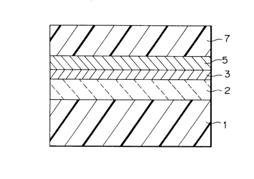
as shown in Fig. 2 were made. In Fig. 2, 1 denotes a
transparent substrate, 2 a transparent dielectric layer,
3 a magneto-optical recording layer, and 5 a metal
reflecting layer.
A disc-like substrate 1 of a polycarbonate (PC)
resin having a diameter of 130 mm and a thickness of
1.2 mm, and having grooves at a pitch of 1.6 ~m, was
mounted in a vacuum chamber of an RF magnetron
sputtering unit (ANELVA Corporation, type SPF-430H)
capable of mounting three targets, and the chamber was
evacuated to less than 5.3 x 10 5 Pa (4 x 10 7 Torr).
A mixed gas of Ar and N2 (Ar:N2 = 70:30) was
introduced into the chamber and the flow rate of the gas
mixture was regulated to a pressure of 1.3 Pa
(10 mTorr). An AlSiN layer (80 nm thick) as the
transparent dielectric layer 2 was deposited by RF
sputtering, using a target of a sintered Al50Si50
(diameter 100 mm and thickness 5mm) and an electrical
discharge at a power of 500 Watts (W) and an RF of
13.56 MHz, while rotating the PC substrate.
Then a TbFeCo alloy layer (30 nm thick) as the
magneto-optical recording layer 3 was deposited on the
AlSiN layer by RF sputtering a target of a Tb21Fe71Co8
`;.
2 o ~ 7 ? ~ ~
-- 13 --
alloy at an Ar gàs pressure of 0.27 Pa (2 mTorr) and an
electric discharge power of 150 W.
Then using targets of Al with a certain number of
Au chips (3 mm square by 1 mm thick) placed on the
target, metal reflecting layers (40 nm thick) 5 having
compositions shown in Table 1 were deposited on the
TbFeCo alloy layer 3 under conditions of an Ar gas
pressure of 0.27 Pa (2 mTorr) and an electric discharge
power of 100 W. The composition of the metal reflecting
layer was controlled by varying the number of the Au
chips on the Al target.
During the deposition of the above layers, the PC
substrate was rotated at a speed of 20 rpm.
Thus, optical recording discs having a structure of
PC substrate(l)/AlSiN(2)/TbFeCo( 3 ) /metal(5) reflecting
layer were obtained.
The C/N ratio and optimum recording laser power of
the optical recording discs were evaluated by a
magneto-optical recording and reproducing unit
(Nakamichi, OMS-1000 type) under the following
conditions. The optimum recording laser power was
determined by varying the power of a laser diode for
recording and selecting the power when the second
harmonics of the reproducing signal are at a minimum.
Recording conditions:
Disc rotation speed: 1800 rpm
Position of recording on disc: 30 mm radius
Recording frequency: 3 . 7 MHz
Applied magnetic field during recording:
500 Oersteds
Reproducing conditions:
Disc rotation speed: 1800 rpm
Laser power for reproducing: 1.2 mW
The results are shown in Table 1.
Comparative example 1 was the same magneto-optical
recording medium as Examples 1 - 4 except that the metal
reflecting layer was an Al layer deposited using an Al
2017~4
- 14 -
target without the Au chips thereon in the same
procedure as that of Examples 1 - 4. The optimum
recording laser power of Comparative example 1 of more
than 20 mW in Table 1 denotes that no reproducing signal
was obtained by recording at the maximum power of the
laser diode of 10 mW and a slight reproducing signal was
obtained by recording at the maximum power of 10 mW and
at a half speed of the above disc rotation speed.
Table 1
Disc Au content of Optimum recording C/N
metal reflecting laser power ratio
layer (at~) (mw) (dB)
Com.Ex.l 0 more than 20 --
Ex.l 3.0 7.5 46.5
Ex.2 5.0 7.0 46.6
Ex.3 15 6.5 46.6
Ex.4 20 5.5 45.9
Com.Ex.2 25 5.0 44.4
On the metal reflecting lay,er of the discs of
Examples 1 - 4 and Comparative example 1, an ultra-
violet ray curable phenol novolak epoxy acrylate resin
was coated by a spin coater and was cured by irradiation
of ultra-violet ray, to form an organic protecting
layer 7 having a thickness of about 20 ~m. These discs
were subject to an accelerated aging test under a
temperature of 80C and a relative humidity of 85% for
1000 hours and evaluated by the increased number of pin
holes. The number of pin holes was not changed in
Examples 3 and 4, was increased by 15 in Example 1 and
by 10 in Example 2. In Comparative example 1, a large
number of pin holes were found and the number thereof
could not be counted. The optimum recording laser power
2017~84
-- 15 --
and C/N ratio of the discs having the organic protecting
layer were measured. In all Examples and Comparative
example, the C/N ratios were not changed from those in
Table l but the optimum recording laser powers were
increased from those in Table l by about 0.8 mW. This
suggests that the organic protecting layer 7 advan-
tageously provides an improved durability but
disadvantageously causes a lowering of the recording
sensitivity.
Example 5
A magneto-optical recording disc was made and
evaluated in the same manner as Examples l - 4. This
magneto-optical recording disc was the same as
Examples l - 4 except that the metal reflecting layer of
Algo 7Au7 2Ti2 1 was formed by an RF sputtering using an
AlAuTi alloy target of a uniform composition having a
diameter of lO0 mm and a thickness of 5 mm in the manner
as Example l - 4.
The optimum recording laser power of the disc was
5. 7 mW and the C/N ratio was 46.8 dB. It is clear from
a comparison with Table l that the recording sensitivity
of the medium of Example 5 (a reflecting layer of an Al
alloy with 7. 2% Au and 2.1% Ti) is as high as that of
Example 3 (a reflecting layer of an Al alloy with as
much as 15% Au) and the C/N ratio of Example 5 was good.
As seen from the above, by a metal reflecting layer
of an Al alloy with Au and optionally Ti, a magneto-
optical recording disc having a superior C/N ratio and
recording sensitivity and a high durability were
obtained. Particularly, when the content of Au or the
total of Au and Ti is in a range of 3.0 at% or more, a
lowering of the optimum recording laser power, i.e., the
improvement of the recording sensitivity, is remarkable
and the C/N ratio is high.
Example 6 - ll and ComParative examples 3 - 4
Magneto-optical recording discs having a structure
of substrate(l)/first transparent dielectric
~.
2~172~4
- 16 -
layer(2)/magneto-optical recording layer(3)/second
transparent dielectric layer(4)/metal reflecting
layer(5)/organic protecting layer(7) were made and the
composition of the metal reflecting layer thereof was
varied (see Fig. 3). The media were evaluated in the
same manner as in Examples 1 - 5.
A polycarbonate (PC) resin disc-like substrate 1
having a diameter of 130 mm and a thickness of 1.2 mm
and having grooves at a pitch of 1.6 ~m was mounted in a
vacuum chamber of an RF magnetron sputtering unit
(ANELVA Corporation SPF-430H) capable of mounting three
targets, and the chamber was evacuated to less than 5.3
x 10 5 Pa (4 x 10 Torr).
A mixture gas of Ar and N2 (Ar:N2 = 70:30) was
introduced into the chamber and the flow rate of the gas
mixture was regulated to a pressure of 1.3 Pa
(10 mTorr). An AlSiN layer (120 nm thick) as the first
transparent dielectric layer 2 was deposited by RF
sputtering, using a target of a sintered A130Si70 (a
diameter of 100 mm and a thickness of 5 mm) and an
electrical discharge at a power of 500 W and an RF of
13.56 MHz, while rotating the PC substrate.
Then a TbFeCo alloy layer (22.5 nm thick) as the
magneto-optical recording layer 3 was deposited on the
AlSiN layer 2 by RF sputtering a target of a Tb21Fe71Co8
alloy at an Ar gas pressure of 0.27 Pa (2 mTorr) and an
electric discharge power of 150 W.
An AlSiN layer (40 nm thick) as the second
transparent dielectric layer 4 was deposited on the
TbFeCo layer 3 in the same manner as the first
transparent dielectric layer 2.
Then using the AlAuTi alloy target of Example 5
[Example 11], or Al targets with a certain number of Au
chips [Examples 6 - 10] or Ti chips [Comparative
example 4] (3 mm square by 1 mm thick) placed on the
target, metal reflecting layers (60 nm thick) 5 having
compositions shown in Table 2 were deposited on the
~ .
20:L~284
- - 17 -
AlSiN layer 4 under conditions of an Ar gas pressure of
0.27 Pa t2 mTorr) and an electric discharge power of
100 W. The composition of the metal reflecting layer 5
was controlled by varying the number of the Au or Ti
chips on the Al target.
During the deposition of the above layers, the PC
substrate 1 was rotated at a speed of 20 rpm.
Comparative example 3 was a magneto-optical
recording disc having the same structure as those of
Examples 6 - 11 except that the metal reflecting layer
was an Al layer deposited using an Al target without the
Au chips thereon in the same procedure as Comparative
example 1.
On the metal reflecting layer 5 of the obtained
discs of Examples 6 - 11 and Comparative examples 3 - 4,
an ultra-violet ray curable phenol novolak epoxy
acrylate resin was coated by a spin coater and was cured
by irradiation of ultra-violet ray, to form an organic
protecting layer 7 having a thickness of about 20 ~m.
The optimum recording laser power and C/N ratio of
the discs were evaluated. The results are shown in
Table 2.
Then the discs were subject to an accelerated aging
test under a temperature of 80C and a relative humidity
of 85% for 1000 hours and evaluated by counting the
increased number of pin holes with the naked eye. The
- results are shown in Table 2.
` 20172g4
- 18 -
Table 2
Disc Composition Optimum C/N Increased
of metal recording ratio number of
reflecting laser pin hole
layer (at~) power (mW) (dB)
Ex.6 Alg9 4Auo 6 9.0 47.2 22
Ex.7 98.8 1.2 8.0 47.5 15
Ex-8 97 3 6.8 47.5 5
Ex.9 95 5 6.3 47.4 2
Ex.10 A185Aul5 6.0 47.0 0
Ex.ll Algo 7AU7.2Ti2.1
Com.Ex.3 Al 9.5 46.7more than
100
Com.Ex.4 99.2 0.8 8.5 47.3 100
From Table 2, it is seen that the magneto-optical
recording disc of Comparative example 3 allowed a
recording, different from Comparative example 1, but
still has a large optimum recording laser power and a
low C/N ratio and particularly, has a poor durability.
The magneto-optical recording disc of Comparative
example 4 has a good optimum recording laser power and
C/N ratio, but a poor durability, as shown in
Comparative example 3.
In contrast, in Examples 6 - 11, by containing
0.5 at% or more of Au in an AlAu alloy of the metal
reflecting layer, the recording sensitivity (optimum
recording laser power), C/N ratio and durability of the
discs were improved and the discs have a high durability
without problems. Particularly when the content of Au
or the total content of Au and Ti is in a range of
1.0 at~ or more, a remarkable improvement of the
recording sensitivity is obtained and the C/N ratio and
durability are good. From the viewpoints of these
20~L72~4
- 19 -
effects, the total content of Au and Ti is particularly
preferably 1.0 to 15.0 at%.
From a comparison of Examples 6 - 11 with
Examples 1 - 5, it is seen that a provision of a second
transparent dielectric layer, although making the layer
structure of the disc slightly complex, allows a
lowering of the optimum recording laser power of more
than 1 mW and an improvement of the C/N ratio of about
0.4 - 1.0 dB, as well as bringing a remarkable
improvement of the durability.
Example 12
A magneto-optical recording disc having the same
structure as that of Example 11 except that the
magneto-optical recordin~ layer was a bilayer comprised
of GdFeCo and TbFeCo layers 3a and 3b was made. The
bilayer of the magneto-optical recording layer was
formed by RF sputtering an alloy target of Gd21Fe55Co24
to deposit a GdFeCo layer (15 nm) 3a on the first
transparent dielectric layer 2 and then an alloy target
of Tb21Fe73Co6 to deposit a TbFeCo layer (20 nm) 3b on
the GdFeCo layer 3a (Fig. 4).
The disc was evaluated in the same manner as
Example 11. The optimum recording laser power was
4.5 mW and the C/N ratio was 47.8 dB. The number of pin
holes was not increased.
By using a bilayer magneto-optical recording layer,
a magneto-optical recording disc having a remarkably
improved recording sensitivity and a high C/N ratio and
durability can be obtained.
Example 13
A magneto-optical recording disc having a structure
of substrate(1)/first transparent dielectric
layer(2)/magneto-optical recording layer(3)/second
transparent dielectric layer(4)/metal reflecting
layer(5)/inorganic protecting layer(6)/organic
protecting layer(7) was made by forming layers from the
first transparent dielectric layer 2 to the metal
`;;
2~317284
- - 20 -
reflecting layer 5 on the substrate 1 in the same manner
as Example ll, and forming an AlSiN layer as the
inorganic protecting layer 6 on the metal reflecting
layer 5 in the same manner as the first and second
transparent dielectric layers 2 and 4 of Example 11,
followed by forming an organic protecting layer (about
20 ~m) 7 on the inorganic protecting layer 6 in the same
manner as the organic protecting layer 7 of Example 11
(Fig. 5).
The disc was evaluated in the same manner as
Examples 6 - 11. The optimum recording laser power was
5.5 mW and the C/N ratio was 47.6 dB, not different from
those of Example 11.
The accelerated aging test was conducted for the
disc of Example 13 together with the disc of Example 11
under the conditions of 80C and 85%RH for 3000 hours.
As a result, in the disc of Example 11, a large number
of pin holes were observed in a non-recording area
around the center of the disc having a flat surface
without grooves. In contrast, in the disc of Example 13
having an inorganic protecting layer, no pin holes were
observed and a further improvement of the durability was
obtained.
Example 14
A double-sided recording disc was made by bonding
two magneto-optical recording discs 10 of Example 13 on
the protecting layer sides thereof with a hot melt
adhesive 8 (Fig. 6).
The evaluation of the disc was conducted in the
same manner as the other Examples. The recording
sensitivity and C/N ratio were the same as those of
Example 13, with differences within the measurement
errors. No pin holes were observed after the same
accelerated aging test (3000 hours) as that for
Example 13.
The bit error rate of the overall recording surface
of the disc was measured, using an error rate tester
2017Z~
- 21 -
(manufactured by TASK Technology), before and after the
above accelerated aging test and the change of the bit
error rate was evaluated. The change was 1.5 times and
1.8 times for respective sides of the disc, both less
than 2 times which is the limit for practical use.
Further, another durability test was conducted for
the disc of Example 14 by a cycle test (ZAD test) in
which the atmosphere starts from 60C and 95%RH and is
varied between 60C and -25C in two days for one cycle,
and 20 cycles were repeated. As a result, the bit error
rates of the respective sides of the disc were not
changed, 4 x 10 6 and 2 x 10 6, before and after the
test. This shows that the disc has a very high
durability.
Examples 15 - 18 and ComParative example 5
The procedures of Examples 1 - 4 and Comparative
example 1 were repeated to make magneto-optical
recording discs having the same structure as those of
Examples 1 - 4 and Comparative example 1 except that the
metal reflecting layer 5 was an AgAu alloy layer formed
by RF sputtering using an Ag target with Au chips placed
thereon and controlling the composition of the AgAu
alloy layer by varying the number of the Au chips on the
Ag target (see Fig. 1). The compositions of the discs
of Examples 15 - 18 and Comparative example 5 are shown
in Table 3.
The evaluation of the discs was conducted in the
same manner as Examples 1 - 4 and Comparative example 1
except that the recording frequency was 2 MHz instead of
3.7 MHz for Examples 1 - 4.
The results are shown in Table 3.
20~7~4
- 22 -
Table 3
Disc Au content of Optimum recordingC/N
metal reflecting laser power ratio
lsyer (atZ) (mw) (dB)
Com.Ex.5 0 more th~n 20 --
Ex.15 2.0 8.5 55.2
Ex.16 5 7,0 55.4
Ex.17 15 6.0 55.3
Ex.18 30 5.5 53.1
On the metal reflecting layer 5 of the discs of
Examples 15 - 18, a W-curable phenol novolak epoxy
acrylate resin was coated by a spin coater and cured by
irradiating with W rays, to form an organic protecting
layer 7 having a thickness of about 20 ~m. The discs
were subject to an accelerated aging test under 70C and
85%RH for 1000 hours. The C/N ratio and the appearance
of the discs of Examples lS - 18 were not changed after
the aging test, and thus the durability and protecting
effect of the metal reflecting layers of Examples were
confirmed.
Examples 19 - 23
Magneto-optical recording discs having the same
structure as those of Examples 15 - 18, except that the
metal reflecting layer of an AgAu alloy further
contained Ti, Ta, Zr or Y, were made in the same manner
as Examples 15 - 18. The metal reflecting layer of an
AgAu alloy containing Ti, Ta, Zr or Y was formed by RF
sputtering using an Ag target with Au chips and chips of
Ti, Ta, Zr or Y placed on the target.
The evaluation of the discs was conducted in the
same manner as Examples 15 - 18.
The results are shown in Table 4.
20172~4
- 23 -
Table 4
Disc Reflectin~ layer Optimum C/N
Au Added element recording ratio
contentElement Content laser
(atZ) (at~) power (mW) (dB)
Ex.19 5 Ti 2 5.5 56.0
Ex.20 5 Ti 4 5.0 55.8
Ex.21 5 Ta 3 5.5 55.4
Ex.22 4 Zr 3 5.5 55.3
Ex.23 4.5 Y 2 5.5 55.8
The same organic protecting layer as that of
Examples 15 - 18 was formed on the discs of Examples 19
- 23 and the accelerated aging test was conducted under
the same conditions as Examples 15 - 18. The C/N ratio
and the appearance of the discs were not changed after
the aging test.
As seen in Examples 15 - 23, a metal reflecting
layer of an AgAu alloy with an Au content of 0.5 at~ or
more allows to provide a magneto-optical recording disc
having a high C/N ratio and recording sensitivity and an
excellent durability and a metal reflecting layer of an
AgAu alloy further containing Ti, Ta, Zr or Y allows a
further improvement of the recording sensitivity.
Examples 24 - 26 and Comparative example 6
Magneto-optical recording media having the same
structure as those of Examples 15 - 23 were made in the
following manner and evaluation of the media was
conducted under the conditions of a recording density
and an accelerated aging test time which were about
double those of Examples 15 - 23.
A disc-like substrate 1 of a polycarbonate (PC)
resin having a diameter of 130 mm and a thickness of
1.2 mm and having grooves at a pitch of 1.6 ~lm was
mounted in a vacuum chamber of an RF magnetron
2Q~i72~4
- 24 -
sputtering unit (ANELVA Corporation, type SPF-430H)
capable of mounting three targets, and the chamber was
evacuated to less than 5.3 x 10 5 Pa (4 x 10 7 Torr).
A mixture gas of Ar and N2 (Ar:N2 = 70:30) was
introduced into the chamber and the flow rate of the gas
mixture was regulated to a pressure of 1.3 Pa
(10 mTorr). An AlSiN layer (80 nm thick) as the
transparent dielectric layer 2 was deposited by RF
sputtering, using a target of a sintered Al30Si70 (a
diameter of 100 mm and a thickness of S mm) and an
electrical discharge at a power of 500 W and an RF of
13.56 MHz, while rotating the PC substrate.
Then a TbFeCo alloy layer (22.5 nm thick) as the
magneto-optical recording layer 3 was deposited on the
AlSiN layer 2 by RF sputtering a target of a Tb21Fe71Co8
alloy at an Ar gas pressure of 0.27 Pa (2 mTorr) and an
electric discharge power of 150 W.
Then using targets of Ag with a certain number of
Au chips or Au and Ti or Ta chips (3 mm square by 1 mm
thick) placed on the target, metal reflecting layers
(40 nm thick) 5 having compositions shown in Table 5
were deposited on the TbFeCo alloy layer 3 under
conditions of an Ar gas pressure of 0.27 Pa (2 mTorr)
and an electric discharge power of 100 W. The
composition of the metal reflecting layer 5 was
controlled by varying the number of the Au, Ti and Ta
chips on the Ag target.
During the deposition of the above layers, the PC
substrate 1 was rotated at a speed of 20 rpm.
Thus, optical recording discs having a structure of
PC substrate(l)/AlSiN(2)/TbFeCo(3)/metal reflecting
layer (5) were obtained (see Fig. 2).
Further on the metal reflecting layer 5, a
W-curable phenol novolak epoxy acrylate resin was
coated and cured by irradiating with W-rays, to form an
organic protecting layer 7 having a thickness of
about 20 ~m (Fig. 2).
~.
20~728~
- - 25 -
The original characteristics of the obtained
optical recording discs were evaluated, and a durability
test of the discs under 80C and 85%RH was conducted for
2000 hours, double that of Examples 15 - 23, and the C/N
ratio and the increase in the number of pin holes were
then determined. The original characteristics of the
discs were evaluated by using a magneto-optical
recording and reproducing unit (Nakamichi OMS-l000 type)
under the following conditions and by varying the power
of a laser diode for recording and selecting the power
at which the second harmonics of the reproducing signal
are at a minimum as the optimum recording laser power.
Then the recording frequency was 3.7 MHz, about double
that of Examples 15 - 23.
Recording conditions:
Disc rotation speed: 1800 rpm
- Position of recording on disc: 30 mm radius
Recording frequency: 3.7 MHz
Applied magnetic field during recording:
500 Oersteds
Duty: 50%
Reproducing conditions:
Disc rotation speed: 1800 rpm
Laser power for reproducing: l.2 mW
The results are shown in Table 5.
Comparative example 6 was a magneto-optical
recording disc having the same structure as those of
Examples 24 - 26 except that the metal reflecting layer
was an Ag layer deposited using an Ag target without the
Au or Ti, Ta chips thereon in the same procedure as
Examples 24 - 26. The optimum recording laser power of
Comparative example 6 of more than l0 mW in Table 5
denotes that no reproducing signal was obtained by
recording at the maximum power of the laser diode of
l0 mW.
In Examples 24 - 26, the number of increased pin
20i7~8~
_ 26 -
holes is slightly large, but even after the accelerated
aging test for 2000 hours, the C/N ratio was not
changed, and the C/N ratio and the recording recording
sensitivity were high enough to be practically used.
Table S
Disc Composition Optimum C/N Increased
of metal recording ratio number of
reflecting laser pin hole
layer (at~) power (mW) (dB)
Ex.24 Agg5AU5 8.0 48.4 14
Ex.25 g95 4 1 48.5 9
Ex.26 Agg2Au5Ta3 6.5 48.Z 12
Com.Ex.6 Ag more than -- more than
10 mW 100
Examples 27 - 35 and ComParative examples 7 - 8
Magneto-optical recording discs having a structure
similar to those of Examples 15 - 26 but including
another transparent dielectric layer 4 between the
magneto-optical recording layer 3 and the metal
reflecting layer 5 were made and evaluated (see Fig. 3).
The transparent dielectric layer (12 nm thick)
4 between the magneto-optical recording layer 3 and the
metal reflecting layer 5 was formed in the same manner
as the transparent dielectric layer 2 between the
substrate 1 and the magneto-optical recording layer 3 of
Examples 24 - 26. The metal reflecting layer 5 had an
AgAu alloy composition shown in Table 6.
The evaluation of the discs was conducted in the
same manner as Examples 24 - 26.
20i~28~
- 27 -
Table 6
Disc Composition Optimum C/N Increase
of metal recording ratio in number
reflecting laser of pine
layer (atZ) power (mW)(dB) holes
Ex.27 g98 2 8.0 48.4 10
Ex.28 Agg5Au5 7.5 48.5 7
Ex.29 Ag85Aul5 7.0 48.2 5
EX.30 g70 30 6.5 47.6 5
Ex.31 Agg5Au4Til 6.5 48.6 2
Ex.32 Ag86Au4Tilo 6.0 47.6 2
Ex.33 Agg3Au4Ta3 6.5 48.2 3
Ex.34 Agg3Au4Zr3 6.5 48.2 3
Ex.35 Agg4Au4Y2 6.5 48.6 2
Com.Ex.7 Ag more than -- 48
Com.Ex.8 98 2 5 47.5more than
100
The disc of Comparative example 7 had the same
structure as that of Examples 27 - 35 but the metal
reflecting layer 5 was an Ag layer formed by sputtering
an Ag target without Au chips or the like. The disc of
Comparative example 8 had the same structure as that of
Examples 27 - 35 but the metal reflecting layer 5 was an
AlTi (Ti: 2 at%) layer (60 nm thick) formed by
sputtering an Al target with Ti chips.
In Comparative example 7 using a metal reflecting
layer 5 of Ag, the recording power was so high that it
could not be determined by the unit for measurement
(maximum power 10 mW), and the number of the pin holes
was greatly increased after the accelerated aging test.
In Comparative example 8, using a metal reflecting layer
of AlTi, the C/N ratio was low and the number of pin
- 20~L7284
- 28 -
holes was remarkàbly increased. In contrast, in
Examples 27 - 35, it was confirmed that the recording
sensitivity and C/N ratio were high, and the durability
was good since the C/N ratio was not changed and only a
slight increase in the number of pin holes was found
after the accelerated aging test for 2000 hours.
It was confirmed from a comparison with Examples 24
- 26 that a provision of a transparent dielectric
layer 4 between the magneto-optical recording layer 3
and the metal reflecting layer S, although making the
construction of the disc slightly complex, remarkably
improves the durability of the disc under a high
temperature and high humidity and improves recording and
reproducing characteristics such as the C/N ratio and
recording sensitivity.
Examples 36 - 4l
Magneto-optical recording discs having the
structure similar to that of Examples 27 - 35 but
further including an inorganic protecting layer 6
between the metal reflecting layer 5 and the organic
protecting layer 7 were made (see Fig. 5) and evaluated
in the same manner as Examples 27 - 35. More
specifically, Examples 36 - 41 was the same as
Examples 28 and 31, except that an AlSiN layer 6 having
a thickness shown in Table 7 was formed in the same
manner as Examples 27 - 35 or a Ti layer 6 having a
thickness shown in Table 7 was formed by RF sputtering a
Ti target under the same conditions as those for the
magneto-optical recording layer of Examples 27 - 35.
The results of evaluation of the discs are shown in
Table 7.
2~7284
_ 29 -
_ ,
Table 7
Disc Composition Inorganic pro- Optimum C/N Increase
of metal tectin~ layer recording ratio in number
reflecting Material Thick- laser of pin
layer ness power holes
(atZ) (nm) (nW) (dB)
Ex.36Agg5AU5 Ti 15 8.048.5 0
Ex.37Agg5AU5 AlSiN 20 7.548.6 0
g95 4 1 Ti 10 6.5 48.6
g95 4 1 Ti 20 7.0 48.70
Ex.40 Agg5Au4Til AlSiN 10 6.5 48.7
Ex.41 Agg5Au4Til AlSiN 20 6.5 48.8 0
By providing an inorganic protecting layer 6, a
magneto-optical recording disc can have a high recording
sensitivity and C/N ratio as well as a further improved
durability. Particularly, a magneto-optical recording
disc having an AlSiN layer as an inorganic protecting
layer 6 can have an improved durability without any
lowering of a recording sensitivity and C/N ratio.
Examples 42 - 43
The same magneto-optical recording discs as
Example 41, except that the thicknesses of the
transparent dielectric layers 2 and 4 were varied, were
made and evaluated (Fig. 5).
The results are shown in Table 8.
20~7~4
- - - 30 -
Table 8
Disc Thickness of Thickness of Optimum C/N Increase in
inorganicInorganic recording ratio number of
protectingprotecting laser pine hole
layer 2 layer 4 power
(nm) (nm) (mW) (dB)
Ex.42 120 30 6.5 48.8 0
Ex.43 120 35 6.5 48.7 0
Example 44
The same magneto-optical recording disc as
Example 41, except that the magneto-optical recording
layer-was a bilayer comprised of GdFeCo and TbFeCo
layers, was made. The bilayer of the magneto-optical
recording layer was formed by RF sputtering an alloy
target of Gd2lFe55Co24 to deposit a GdFeCo layer (15 nm
3a on the first transparent dielectric layer 2 and then
an alloy target of Tb21Fe73Co6 to deposit a TbFeCo layer
(20 nm) 3b on the GdFeCo layer 3a (see Fig. 4).
The disc was evaluated in the same manner as
Example 41. The optimum recording laser power was
5.0 mW and the C/N ratio was 49.0 dB. The number of pin
holes was not increased.
By using a bilayer magneto-optical recording layer,
a magneto-optical recording disc having a remarkably
improved recording sensitivity and a high C/N ratio and
durability is obtainable.