Note: Descriptions are shown in the official language in which they were submitted.
2017388
- MEASURING AND CONTROLLING THE l~llCKNESS OF A
CONDUCIIVE COATING ON AN OPTICAL FIBER
This invention relates to a method used in making a coated elongated
inml~tQr, such as an optical fiber.
Baclcground of the Invention
Performance characteristics of optical fibers can be degraded by
5 environmental elements. For example, the interaction of water with the surface of a silica
fiber produces surface modifications which can reduce the strength of the fiber. Also over
a period of time, hydrogen can diffuse into an optical fiber and increase the optical loss in
a signal carried by that optical fiber.
In order to prevent such interactions, a coating can be applied to the fiber
10 for plevell~illg deleterious environmental elements from interacting with the fiber. Ideally
such a coating acts as an impenetrable hermetic barrier between the fiber and the
environment. One such coating, e.g, a carbon coating, is applied under stable ambient
conditions to the outer surface of a silica cladding of the fiber by inducing decomposition
of a suitable carbon containing organic precursor gas, e.g, acetylene, to form a thin carbon
15 film on the fiber surface. For OL)~i~llUIll results, the carbon coating must be applied at a
particular thickness within close tolerances. If the coating is too thin, it does not
sufficiently limit the penetration of the undesirable ellvirolllllental elements, such as water
and hydrogen. On the other hand, if it is too thick, fiber strength can be reduced by
microcracks which can form in the carbon coating when the fiber is under high tensile
20 force.
A need therefore has arisen for a dynamic method to measure and to
control the thickness of the coating being applied to the fiber. The method should allow
continuous production of the fiber and avoid any direct contact with the fiber. Any
interruption of the continuous drawing process is intolerable. Physical contact with an
25 unjacketed optical fiber can damage the surface and reduce the tensile strength of the
fiber. In the prior art, however, thickness of a coating has been measured by static off-
line metrology, eg., by electron microscow or by c~ ul~tion based on a direct current
measurement of resistance in an electrical circuit. These prior art
-1-
, ~
2017~88
- methods require either the interruption of the drawing process, physicai contact with the
unjacketed optical fiber, or both.
S..mn~ry of the Invention
These and other problems are solved by a new method for making an
S optical fiber. This manufacturing method includes the steps of: depositing a coating on
the moving optical fiber and by means of a non-contact cle~ liolllagnetic field measuring a
value of effective radio frequency conductance of the coating for dynamically controlling
the thickness of that coating being deposited on the optical fiber.
In accordance with one aspect of the invention there is provided a method
10 for determining the thickness of a conductive coating on an elongated body of a dielectric
material, which includes the steps of (a) establishing an electromagnetic field in a section
of a hollow metallic waveguide, (i) said waveguide section being terminated by matched
terminations on opposite ends thereof, (ii) said electromagnetic field being established by
said matched terminations, and having a frequency of oscillation in the radio frequency
range of from 10 MHz to 150 GHz, (iii) said waveguide section having an opening in each
of the opposite broad walls thereof pe~ g passage of an elongated body transverse of
the waveguide section in subst~nti~l alignment with the electric field component of the
clc~lolllagnetic field and without any physical contact with the walls of the waveguide
section, (b) moving a conductively coated ek ng~ted dielectric body through said openings
20 so that it passes through the electromagnetic field, and (c) in response to a change in the
electromagnetic field, generating a signal represçnt~ive of the thickness of the conductive
coatings.
Featured within the manufacturing method is a method for measuring the
thickness of a conductive coating on an in~ tor, e.g., carbon on an optical fiber.
25 Measuring the thickness of the coating includes the following steps. A radio frequency
electromagnetic field is established by an input signal. The coated insulator is moved
through the energized electromagnetic field at a position where the electric field is
sufficiently strong to create a useful output signal. The coating on the inc-ll~tQr is
oriented with respect to the electric field or a component thereof so that its interaction
30 with the conductive coating increases ~ liccion loss from input to output. An output
signal is extracted from the electromagnetic field at a point where the output signal can
be cletecte~ Such point is remote from the fiber location. Extraction can be
~ .
2017~88
accomplished by either an electric field probe or a magnetic field probe. From changes in
the output signal with respect to a predetermined standard, the effective radio frequency
conductance of the conductive coating is determined. Thickness of the coating isdetermined from the conductance data.
S The following advantages are achieved by the folegoillg method. The
coated in~ tor continuously moves through the apparatus for measuring without any
physical contact. No interruption of the production process occurs. From the thickness
determination, signals are generated for dynamically controlling the coating process to
maintain a desired thickness tolerance.
The general principles here stated can be applied over a wide range of
radio frequencies, typically from about 10 MHz to 150 GHz, and can be applied to a wide
range of coating configurations by appropliately selecting a frequency range andequipment that is compatible with the selected frequency range.
-2a-
- 201~3~8
-
Brief De~cription of the Drawin~
A better understanding of the invention may be derived by
reading the subsequent detailed description thereof with reference to the
attached drawing wherein:
FIG.lis a schematic diagram of an arrangement for drawing an
optical flber and of apparatus for making measurements and controlling the
drawing operation and the coating process;
FIG.2is a diagram of a section of optical fiber without its
polymeric jacketing;
FIG.3is a diagram of a section of optical flber coated with a
conductive carbon coating;
FIG.4is a schematic diagram of an arrangement for measuring
the thickness of the conductive carbon coating on the optical flber;
FIG.5is a perspective drawing of the vectors of an incident
electromagnetic wave and its resulting reflected electromagnetic wave
produced at a short circuit termination;
FIG.6is a series of curves representing output energy versus
frequency for different measurements taken on an optical fiber;
FIG.7is a schematic diagram of another arrangement for
measuring the thickness of the conductive coating on the optical fiber;
FIG.8is a schematic diagram of a third arrangement for
measuring the thickness of the conductive coating on the optical fiber;
FIG.9is a schematic diagram of a fourth arrangement for
measuring the thickness of the conductive coating on the optical flber;
FIG.lOis a transmitted power loss versus conductance, or
thickness, characteristic for an exemplary coated flber;
FIG.llis a schematic diagram of a flfth arrangement for
measuring the thickness of the conductive coating on the optical flber
FIG.12 shows a cross-section view taken from the arrangement
of FIG. 11;
FIG. 13 is a schematic diagram of a sixth arrangement for
measuring the thickness of the conductive coating on the optical flber;
FIG.14 shows a cross-section view taken from the arrangement
of FIG.13;
FIG.15is a schematic diagram of a seventh arrangement for
measuring the thickness of the conductive coating on the opti~al fiber; and
- Z017388
FIG. 16 is a schematic diagram of an eighth arrangement for
measuring the thickness of a conductive coating on the optical fiber.
Detailed De~cription
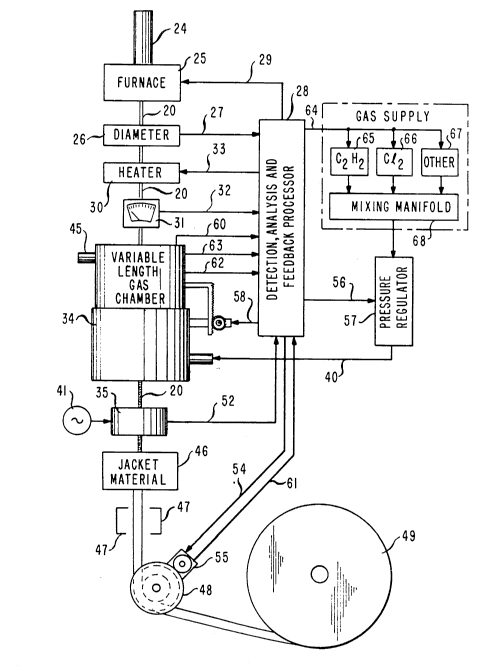
Referring now to FIG. 1, there is shown a diagram of an
5 exemplary equipment for drawing an optical fiber 20 from a preform 24.
The preform may include silica glass with predetermined dopants which will
form an optical fiber having a low loss optical core section that is
surrounded by a cladding section. The core and cladding sections have
different indices of refraction so that light transmitted axially along the core10 is retained within the core because of internal reflections and/or
confinement which occur due to the stratification of the refractive indicies.
A furnace 25 surrounds at least the lower end of the preform 24
and heats that end to its melting or softening temperature. The fiber 20 is
drawn from the end of the preform 24 at a velocity, or rate, that is known
15 to produce the fiber 20 with a predetermined diameter. Generally the fiber
is drawn from the preform at a controlled steady temperature and velocity.
Other combinations of temperature and velocity, or rate, of the draw can be
used for producing fibers with the same diameter.
During the drawing operation, the fiber 20 moves through a
20 diameter gauge 26 which produces on a lead 27 a signal representing the
diameter of the fiber. That signal is forwarded to an input of a detection,
analysis and feedback processor 28. A control signal produced by the
processor 28 is carried by a lead 29 for controlling the temperature of the
furnace 25.
Thereafter the fiber 20 moves along through an optional heater
30 and thermometer, or pyrometer, 31 for supplementing the residual heat
in the fiber 20, if desired, and monitoring the temperature of the fiber 20.
Temperature measured by the thermometer 31 is applied through a lead 32
to the processor 28, which produces a signal on a lead 33 for controlling the
30 temperature of the heater 30. In a variable length, or telescoping, chamber
34, an exemplary mixture of acetylene precursor gas together with chlorine
and an inert gas, such as nitrogen, argon, Gr helium, is applied to the hot
moving surface of the fiber 20 for inducing decomposition of the acetylene
precursor gas and depositing a conductive carbon coating uniformly around
35 the periphery of the fiber. Chlorine is used as a getter for free hydrogen.
Length of the chamber 34 is transmitted via lead 60 to +he processor 28.
The coating deposition process occurs in controlled ambient conditions,
2017388
which typically are stable. While the fiber is moving and without it
contacting any apparatus, the thickness of the exemplary conductive carbon
coating is continuously controlled within tight tolerances to effectively
hermetically seal the optical fiber 20 from any subsequent contact with
5 either water or hydrogen during fabrication, installation, or use of the fiberin a transmission system. At the same time, vulnerability of the coating to
cracking under tensile load due to excessive coating thickness is limited to
maintain an acceptable level of fiber strength.
Referring now to FIG. 2, there is shown a diagram of the bare
10 optical fiber 20 including a center core 22 and cladding 24. Although not
shown in FIG. 2, there may be more layers than the core and single layer of
cladding for the bare optical fiber.
Referring now to FIG. 3, there is shown a diagram of the optical
fiber 20 coated with a thin layer of carbon 27, as represented by dots
15 overall.
After the carbon coating is applied to the moving fiber 20 of
FIG. 1, the coated fiber moves on through a radio frequency resonant cavity
35 for measuring the thickness of the carbon coating. Radio frequency is an
electromagnetic wave frequency intermediate between audio frequency and
20 infrared frequency. A cavity in the microwave range of frequencies has been
used successfully because of component sizes and availability. A microwave
is a very short wavelength electromagnetic wave, typically less than thirty
centimeters in wavelength. Upon exiting from the resonant resonant
frequency cavity 35, the fiber 20 moves on through one or more vessels 46
25 which are filled with ultraviolet light curable liquid materials that are
subsequently transformed into polymeric solids for jacketing the fiber 20 to
protect its surface from future mechanical damage resulting from incidental
or accidental contact. This transformation to the polymeric solid is made
by a set of lamps 47 applying ultraviolet light. Once the jacket is formed on
30 the fiber 20, it is wound about a capstan drive 48 and then onto a reel 49
for storage and for convenience of handling until the flber is installed in a
transmission system. Speed of the capstan 48 and the fiber are sent to the
processor 28 via a lead 61.
Two exemplary subsystems control the previously described
35 optical fiber drawing operation. The first control system, including the
diameter gauge 26, determines the diameter of the fiber by a measurement
made in an optical chamber and by analysis in the processor 28 converts
- 2017388
such measurement into an analagous control signal. This flber diameter
control signal is applied by way of the lead 29 to the furnace 25 for
adjusting the furnace temperature and/or by way of a lead 54 to the
capstan drive control 55 for adjusting the drawing speed so that the fiber
5 diameter is kept within predetermined tolerances. Controlling fiber
diameter by operation of the furnace and the drawing speed are described
in detail in a textbook, entitled "Optical Fiber Telecommunications" edited
by S. E. Miller et al., Academic Press, Inc., 1979, pp.263-298.
Another control system measures and controls the thickness of
10 the carbon coating that is applied to the surface of the moving optical fiber20 without physically contacting the unjacketed fiber. This method for
measuring and continuously controlling the thickness of the carbon coating
operates on one or more of the following parameters: fiber temperature,
acetylene gas pressure, time the fiber is exposed to acetylene, or
15 concentration of acetylene gas; and is an example of the new method of the
invention which is described in detail hereinafter. Pressure in the chamber
34 is transmitted by way of a lead 62 to the processor 28. A control signal
for changing the pressure is sent from the processor 28 via a lead 56 to a
pressure regulator 57. An indication of the concentration of the acetylene
20 gas is forwarded from the chamber 34 by way of a lead 63 to the processor
28. A control signal or control signals for changing the mixture of gases is
transmitted from the processor 28 via a lead 64 to gas supply valves 65,66
and 67. The gases are mixed in a manifold 68 and delivered through the
pressure regulator 57 and supply line 40 to the gas chamber 34. The gases
25 exit the gas chamber 34 by way of an exhaust fitting 45. Although the
cavity 35 is shown preceding the ultraviolet light curable jacketing supply
vessels 46, the cavity 35 could be located after the vessels 46 and the set of
lamps 47.
Referring now to FIG. 4, there is shown a detailed perspective
30 view of the resonant cavity 35. FIG. 4 shows an exemplary resonant cavity
for operation in the microwave frequency range. Shown in FIG. 4 is a
section of hollow rectangular microwave waveguide 37, which has a length
equal to a half guide wavelength at the operating frequency. Each end of
the waveguide section is shorted by one of the conducting plates 38 and 39.
35 A microwave frequency input signal, produced by a fixed or swept frequency
signal generator 41, is coupled through a coaxial line 42, a connector 43, and
an opening through the shorting plate 38 to a loop 44 of the center
2017388
conductor to ground. This magnetic input loop is positioned inside of the
resonant cavity to energize a resonant electromagnetic field in response to
the applied input signal. Power levels of the input signal typically can be in
the range of a fraction of a milliwatt to about 100 mw.
According to the standard adopted for FIG. 4, the array of
arrows represent the electric field vectors in the resonant cavity at
resonance. These electric field vectors present an instantaneous condition
of a continuously alternating electric field. Longitudinally from the input,
the amplitude of the electric field represents a standing wave that increases
10 from zero at the input shorting plate 38 to a maximum amplitude at the
center of the cavity. As shown on an axis along the bottom of the cavity,
there is shown a scale marking off a half guide wavelength ~g/2 between
the input shorting plate 38 and the output shorting plate 39. The
amplitude of the electric field decreases to zero at the output shorting plate
15 39. Although the length of waveguide section 37 is shown as one half guide
wavelength at the operating frequency, other multiples of a half guide
wavelength can be used.
At the center cross-section of the cavity, there are shown two
intersecting planes of arrows representing the electric field for the standing
20 wave. This electric field has a maximum amplitude at or near the center of
the cavity and an amplitude decreasing to zero at both sides of the
waveguide.
A coated optical fiber moves through openings cut into the top
and bottom walls of the section of waveguide. These openings are
25 positioned opposite each other so that the optical fiber is readily threaded
therethrough and moves continuously without physically contacting the
waveguide structure. The openings are placed where the electric field has
sufficient strength to provide a useful signal and is sufficiently uniform
across the opening to make convenient measurements on the moving fiber
30 during the fiber coating operation.
Although it is not shown in FIG. 4, there is a magnetic field
which exists concurrently with the electric field. Such magnetic field is
directed at a right angle with respect to the direction of the electric field.
Together the electric field and the magnetic field make up an
35 electromagnetic field within the resonant cavity in response to the
energizing input signal.
- 2017~88
An output signal can be extracted from the resonant cavity by
either an electric field probe or a magnetic field probe. In either case the
probe is positioned so that it interacts with the appropriate field where the
field strength is sufficient to produce a useful output signal.
As an example in FIG. 4, consider that an output signal is
extracted from the cavity by an output magnetic field loop 50 that is
inserted into the cavity through the output shorting plate 39. This output
coupling loop is formed, e.g., by bending the center conductor of a coaxial
connector 53 to the output shorting plate 39. Coaxial line 52 transmits
10 output signals from the output coupling loop 50 and the connector 53 to a
detection, analysis and feedback processor 28.
It is important to emphasize that although the energy insertion,
or input, coupling loop 44 and the energy extraction, or output, coupling
loop 50 are shown as magnetic field probes positioned for optimum magnetic
15 field strength, they may be replaced by input and output electric field
probes appropriately positioned for an optimum electric field. As an
alternative to the coaxial probe arrangement, other waveguide transmission
media can be substituted for the connectors 43 and 53 by coupling through
appropriate holes in the shorting plates 38 and 39.
Referring now to FIG. 5, there is shown a graph of vectors
representing the electromagnetic energy at the shorting plate 39 of FIG. 4.
At the left of the origin of the three dimensional x, y, z axis, there are an
incident electric field vector Ej, an incident magnetic field vector Hj, and a
velocity vector ~j for the incident electromagnetic wave. It is noted that the
25 electric field vector is oriented in the positive vertical direction and that the
magnetic field vector is oriented horizontally on the three dimensional axis.
When the incident wave reaches the output shorting plate 39 located at the
origin of the horizontal axis, a reflected wave is produced. Since there is a
short circuit, the effective voltage is zero and the reflected electric field Er30 is oriented in the negative vertical direction. Its magnitude equals the
magnitude of the incident electric field Ej.
At the same location, the incident magnetic field Hj also is
reflected. For the reflected magnetic field Hr~ polarity is the same as the
incident magnetic field Hi, but amplitude is doubled because of the output
35 shorting plate 39. Also the reflected velocity vector 'Yr is reversed in
direction from the incident velocity vector yj.
- 2017388
Exemplary input and output magnetic coupling loops 44 and 50
of FIG. 4 are oriented to couple energy into and extract energy from the
resonant cavity at or near the points of maximum magnetic field or at
points with sufficient magnetic field strength to produce a useful signal at
5 the output coupling loop 50.
The exemplary detection, analysis and feedback processor 28 of
FIGs. 1 and 4 performs multiple functions. Among those functions are: (1)
the production of an output signal power versus frequency characteristic
curve for the resonant cavity 35, (2) comparing the output signal power
10 versus frequency characteristic curve to a reference characteristic curve, (3)
determining the difference between the output signal characteristic and the
reference characteristic curve, (4) by way of a lead 56 sending a control
signal related to that difference to a control element 57 of FIG. 1 for
changing the flow of or the partial pressure of acetylene precursor gas, (5)
15 by way of the lead 54 for changing the speed of the drawing operation to
control the flber temperature as it enters the acetylene chamber, (6) by way
of a lead 58 for changing the length of the chamber 34 to control the time of
exposure to the acetylene, and (7) by way of the lead 33 for changing the
temperature of the fiber and the coating on the fiber. The adjustments of
20 these aforementioned coating process parameters are made for changing the
rate at which the carbon coating is deposited on the moving flber. To
control any specific coating process, one or more of these parameters is
controlled.
Referring now to FIG. 6, there is shown a plot of the output
25 energy versus frequency response curve for three different resonant
conditions of the cavity 35 of FIG. 4. In FIG. 6 a narrow, spiked response
curve 76 represents the output signal energy versus frequency for the empty
cavity 35 or for the cavity 35 with an uncoated optical fiber 20 inserted
therein. Since the optical flber 20 is fabricated basically in silica, a
30 dielectric, the flber is an electric insulator, or nonconductor, and causes very
little effect on the empty cavity response curve. Response curve 76 is a
useful reference for control purposes.
Two other response curves 78 and 80 represent curves of the
desired upper and lower limits on the thickness of the carbon coating which
35 is deposited on the optical fber 20 of FIG. 4. Because carbon is conductive
and because the coating is jubstantially aligned with the electric field in the
ca~-ity, that field induces a current in an axial direction along the
g
2017~88
conductive carbon coating on the fiber. Conductivity is a number
proportioned to the current from one face of a unit cube of the coating
material to the opposite face of that cube when a unit potential difference is
maintained between the two faces. Being a conductor, the carbon coating is
5 capable of carrying an electric current. Such a current alternates in
direction at the frequency of the applied electric field and creates a
magnetic field around the fiber 20. This action distorts the electromagnetic
field in the cavity and dissipates or absorbs power. As a result, the output
energy versus frequency curve is reduced in amplitude and is spread out
10 from the shape of the narrow empty cavity response curve 76, and the
resonant frequency changes. A continuous family of curves results. Only,
three curves of the family are shown. By calibrating the resulting response
curves for the desired range of conductance and therefore carbon thickness,
the output response curves 78 and 80 and others of the family are
15 subsequently useful with reference to the curve 76 for measuring the
thickness of the carbon coating as it is deposited on the optical fiber 20.
Typically conductance is a ratio of the current carried by the coating to the
applied electromotive force (reciprocal of resistance) at d.c. For our
purpose, we are measuring an effective radio frequency conductance.
The detection, analysis and feedback processor 28 analyzes the
output energy versus frequency data continuously during a fiber drawing
operation. From the values of amplitude and frequency in comparison with
those of the reference curve, the processor 28 determines both the quality
factor Q of the cavity and the conductance of the coating. Such a
25 conductance determination or measurement is readily convertible to
thickness data of the coating and to a determination of whether or not the
thickness data is within the desired limits. As a result of the processing, the
processor 28 generates a signal which when fedback to control the coating
process maintains the carbon coating thickness within the desired limits by
30 controlling one or more of the process parameters: fiber temperature,
precursor gas density, fiber exposure time, or precursor gas pressure.
Referring now to FIG. 7, there is shown another configuration of
a resonant cavity 90. Except for the round cylindrical shape of the cavity
90, the arrangement and operation of the detect,ion, analysis and feedback
35 processor of FIG. 7 are similar to the apparatus of FIG. 4. The optical
fiber 20, coated with carbon, moves through the cavity 90 in a path so that
the coating is aligned with the energized electric field in the cavity. For the
- 10-
2017388
fiber 20, entrance and exit openings in the cavity 90 are located at or near
the position of sufficient electric field strength to produce a detectable
output signal. Thickness of the carbon is controlled by a feedback control
signal, as described previously.
Referring now to FIG. 8, there is shown another arrangement for
determining the thickness of the carbon coating on the moving optical fiber.
In FIG. 8 there are two round cylindrical cavities 110 and 112 with an
intercoupling section 115. When the signal source 41 applies an alternating
current signal through the line 42 and the input coupling loop 44 to the
10 cavity 110, an electromagnetic field is established therein. Some of the
energy from the electromagnetic field in the first cavity 110 is coupled
through the coupling section 115 into the second cavity 112. From the
second cavity, output signal energy is coupled into the output coupling loop
50 and is transmitted to the detection, analysis and feedback processor 28.
The carbon coated optical fiber 20 moves through an entrance
opening into the second cavity 112, the coupling section 115 and the first
cavity 110 and out from an exit opening. Thickness of the carbon coating is
determined by the same procedure as previously described. Thickness is
measured by the processor 28 which also determines a control signal that
20 controls the carbon depositing operation, as illustrated in FIG. 1.
Referring now to FIG. 9, there is shown a carbon coated optical
flber moving through longitudinal slots 130 and 132 in a section of
waveguide 135. From the source 41 and the line 42, the waveguide is
energized with a propagating electromagnetic field. Slots 130 and 132 are
25 cut in the centerlines of the opposite broad faces of the section of
waveguide. The slots should be as narrow as reasonably possible consistent
with the flber never contacting the slot boundaries.
For convenience of available parts and the sizes of those parts, a
section of WR90 waveguide and a klystron oscillating at 10.5 GHz were
30 chosen for the arrangement. A crystal diode is used for the detector at the
output end of the waveguide 135. Matching sections are used for
connecting the klystron and the detector to the section of waveguide. At
low incident power levels, e.g., less than 100 microwatts, the output current
of the detector is proportional to the square of the electric field in the
35 waveguide. That output current is therefore proportional to output power.
The foregoing specific items and parameters are mentioned by way of
example. Other sizes, frequencies and power levels also are useful.
- 11 -
2017388
As previously mentioned, the input signal, applied by the
klystron in FIG. 9, creates a propagating electromagnetic field in the section
of waveguide. In the unlikely event that the arrangement is perfectly
matched, the magnitude of the time averaged vertical electric field is
5 constant along the entire axis of the section of waveguide 135 in the absence
of the coated fiber. In that case the longitudinal position of the fiber is not
important. In the more likely event that the arrangement is mismatched,
there are standing waves present and therefore at least a partially resonant
condition in the section of waveguide 135. In the mismatched arrangement,
10 there are positions of greater electric field strength where more power is
absorbed by the conductive coating. A deliberate mismatch can be created
by tuning screws and/or irises in the waveguide. In this mismatched case,
the fiber is deliberately located in a longitudinal position coincident with an
electric field maximum which corresponds to a minimum longitudinal field
15 gradient.
When the fiber 20, with the conductive carbon coating, moves
through the waveguide, the conductive coating will interact with the electric
field component which is parallel with the axis of the fiber. Transmitted
power is reduced by the creation of an alternating current in the carbon
20 coating. The amount of power lost is a function of the conductance of the
carbon coating on the fiber. For a uniform outside diameter optical fiber,
conductance of the carbon coating depends upon the conductivity of the
carbon and the carbon coating thickness, which is a variable.
Thus depending upon the variable thickness of the carbon
25 coating, the detection and analysis processor 28 will measure a variable
transmission loss for a specific constant input signal power at a given
frequency.
FIG. 10 shows the result of measurements 134, 136, 137, 138 and
139 of transmitted power loss versus conductance or thickness of some
30 practical examples of carbon coatings.
Referring now to FIG. 11, there is shown a section of a coaxial
transmission line 140 having an outer cylinder conductor 141 and a center
conductor 142 separated by a dielectric 144. When this coaxial transmission
iine 140 is energized by an alternating current signal source 41, an
35 electromagnetic field is established along its length. Detection, analysis and
feedback processor 28 de~;ermines the magnitude of the output signal at the
far end of the section of coaxial transm}ssion line 140. Along a selected
- 12 -
2017388
diameter of the coaxial transmission line 140, there is a hole 146 cut all of
the way through the coaxial transmission line. The optical fiber 20 to be
measured moves through the hole 146 during the fiber drawing operation.
Since the energized electromagnetic field establishes a radial
5 electric field, as shown in the cross section of FIG. 12, there are componentsof that electric field which are oriented more or less parallel with the
coating on the flber 20, as shown in FIGS. 11 and 12. The conductive
carbon coating will have an alternating current induced by the components
of the radial electric field. Thus power is absorbed or dissipated by the
10 carbon coated fiber, and the resulting reduction of output signal power is
measured by the detection, analysis and feedback processor 28.
Referring now to FIG. 13, there is shown a coaxial resonator
arrangement 150 for measuring and controlling the thickness of the carbon
coating on the optical flber 20. An outer concentric conductor 151 and a
15 center conductor 152 are separated by a dielectric 154. Shorting plates 155
and 156 are affixed to each end of the coaxial resonator 150. A center hole
157 is cut through the entire transmission line arrangement along the center
axis of the center conductor 152, as shown in FIG. 14. The coaxial
resonator arrangement 150 of FIG. 13 is energized by a source of alternating
20 current signals 41 to create an electromagnetic field indicated by arrows in
the dielectric 154.
During a drawing operation for the fiber 20, the portion of the
electric field which is aligned with the axis of the fiber 20 induces an
alternating current in the conductive carbon coating on the moving fiber.
25 Detection, analysis and feedback processor 28 measures the thickness of the
carbon coating and produces a signal which controls the carbon deposition
process.
In FIG. 15 the measuring arrangement 170 includes a conductive
chamber 171 and a conductive coil 172, affixed only at one end 173 to the
30 conductive chamber 171 and generally separated from the chamber by a
dielectric 174, such as air. The coil 172 can be fabricated from a
superconductor material. By energizing the coil 172 with a radio frequency
signal from a source 41 using an input coupling loop 176, an electromagnetic
field is established within and along the coil 172. With proper design of the
35 arrangement 170, the alternating electric fleld component is strong along
the center axis of the ccil 172, as shown bv the arrows directed along the
center axis. The carbon coated fiber 20 mo-res through the electric field and
- 13 -
2017388
absorbs power from it. Detected power is extracted from the resonator by
way of an output coupling loop 177. Electrical coupling can be substituted
for the input and/or output magnetic coupling loops. The transmission
response is related to conductance of the carbon coating. Detection,
5 analysis and feedback processor 28 determines the thickness of the
conductive carbon coating and develops a signal for controlling the carbon
deposition process.
In FIG. 16 the measuring arrangement 180 includes a circular
electric TEol mode resonant cavity 181 operated in the millimeter
10 wavelength band so as to develop a circumferential electric field of sufficient
magnitude at the surface of the optical fiber 20 to permit significant
interaction between the conductive coating around the periphery of the
fiber and the resonant cavity behavior. Here to assure TEo1 mode
operation, the cylindrical wall 183 can be an anisotropic conductor, i.e., one
15 that favors circumferential wall current flow and discriminates against axialwall current flow, such as described by S. E. Miller in U.S. patent 2,848,696.
Other higher order circular electric modes can also be used in the cavity.
In order to assure efficient launching and detection of the TE
mode and discrimination against other unwanted modes, antiphased
20 magnetic probes - in the form of small waveguide coupling holes 184 - have
been introduced into the waveguide cavity short circuit end plates 185 and
186. The antiphase arrangement in this example is illustrated by feeding a
microwave source 41 into the difference port ~ of a hybrid junction and
waveguides 188 and by extracting output signals from the cavity via the
25 waveguides 18~ and another hybrid. The sum ports ~ are terminated by
termination elements 187.
As in the prior examples discussed, the resonant cavity behavior
is that shown in Fig. 6. Output energy is coupled through the difference
port ~ and the lead 52 to the detection, analysis and feedback processor 28
30 for measuring and controlling the thickness of the coating on the optical
fiber 20.
To minimize undesirable effects caused by ambient changes, we
have used several techniques such as: practicing the fiber drawing process
and the coating process in a stable controlled environment; using a highly
35 stable oscillator in a temperature controlled environment for the
propagating electromagnetic field measurement set up on FIG. 9; using a
Pound stabilizer, such as described by T. H. Wilmshurst, "Electron Spin
- 14 -
-- 2017388
Resonance Spectrometers", Plenum Press, New York, pages 199-204; using a
stable power supply; using a mechanical configuration which minimizes
distortion of the waveguide; using coaxial cable sections that produce no
more than a small phase shift on flexing; using low thermal expansion
5 waveguide sections; using minimum length microwave paths; and using a
two arm system fed by a common source including two identical waveguide
sensor systems - one as a reference, the other for measuring the effect of the
coated fiber on the output power. Whether these techniques are used or
not depends upon the sensitivity required and the severity of ambient
10 changes in the test environment.
All of the previously described two port devices have single port
analogs that can utilize reflectometers or circulators to accomplish the same
functions.
Dynamic control of the thickness of the coating deposited on the
15 optical fiber is achieved by sensing and adjusting one or more of the
following four parameters: (1) the temperature of the fiber entering the
precursor gas chamber; (2) in the precursor gas chamber, the concentration
of the acetylene gas including the carbon atoms to be deposited; (3) the
acetylene gas pressure in the precursor gas chamber; and (4) the time of
20 exposure of the hot fiber to the acetylene gas in the chamber. Upon close
analysis, other arrangements which might: (1) move the position of the
precursor gas chamber; (2) change the length of the precursor gas chamber;
(3) change the mixture of the gases; (4) vary the speed of the fiber draw; or
(5) alter the temperature of the furnace - fundamentally alter one or more of
25 the four described parameters of the manufacturing process.
Thus there has been described a method for measuring and
dynamically controlling the thickness of a thin carbon coating deposited on
a moving optical fiber. None of the arrangements for performing these
methods of measuring and controlling physically contacts the fiber or the
30 coating during the manufacturing operation. All of the described methods
together with other methods made obvious in view thereof are considered to
be covered by the appended claims.