Note: Descriptions are shown in the official language in which they were submitted.
2~7~L09
PHA.21-501 1 23.04.1990
Fluorescent lamp controllers with dimming control.
This invention relates to fluorescent lamp
controllers and dimming controls for use therein and more
particularly to the provision of a dimming control which
provides protective isolation between input terminals and
lamp energizing circuitry and which facilitates accurate
and safe control of light intensity over a wide range. The
invention provides dimming controls which are efficient and
highly reliable and are readily and economically
manufacturable.
Prior art references relating to fluorescent lamp
controllers are reviewed in the introductory portion of the
specification of an application of Mark W. Fellows, John
M. Wong and Edmond Toy, U.S. Serial No.219,923, filed July
15, 1988, the disclosure of which is incorporated by
reference. Such prior art references include the Wallace
U.S. Patent No. 3,611,021, the Stolz U.S. Patent No.
4,251,752, the Stupp et al. U.S. Patent No.s 4,453,109,
4,498,031, 4,585,974, 4,698,554 and 4,700,113, and the
Zeiler U.S. Patent No. 4,717,863, relating to various forms
of SMPS (Switch Mode Power Supply) circuits operative at
high frequencies to obtain higher efficiency and other
advantages in the energization of fluorescent lamps. The
prior art also includes disclosures of circuits for control
of the energization of fluorescent lamps to control
intensity and effect dimming of the lamps when desired.
This invention was evolved with the general object
of providing a dimmer control for use with fluorescent lamp
controllers and which is operative to control light
intensity over a wide range while having isolation and
2017409
PHA.21-501 2 23.04.1990
other protective features and while being readily and
economically manufacturable. It is also an object of the
invention to provide a dimmer control having features such
as to obtain high efficiency and very safe and reliable
S operation.
In the development of the invention, consideration
has been given to the use of various possible dimming
circuit arrangements and important aspects of the invention
relate to the recognition of potential problems with such
arrangements as well as in the recognition of features
which are usable to advantage. A further specific object of
the invention is to provide a dimmer control which is
usable with and readily connectable to controllers such as
disclosed in the aforementioned Fellows et al. application
and which retain all of the advantageous features thereof
so as to be fully compatible therewith.
The Fellows et al. system has many advantageous
features including features which allow for control of
intensity and which can be used for dimming, although no
specific disclosure is contained in the application. In the
Fellows et al. system, an output circuit which operates as
a tuned circuit couples the output of a variable frequency
DC-AC converter circuit to a fluorescent lamp load. A
control circuit operates upon energization of the
controller to operate the DC-AC converter at a certain high
frequency which is well above a no-load resonant frequency
of the output circuit and above a frequency that at which
the output voltage would be sufficient for ignition. Then
the control circuit operates in a ignition phase in which
it gradually reduces the frequency until ignition occurs.
Thereafter, the control circuit operates in an operating
phase in which it automatically controls lamp current
through control of the frequency of operation of the DC-AC
converter.
Another feature of the Fellows et al. controller
relates to the connection of the resonant capacitor in
parallel relation to the fluorescent lamp load and a
transformer winding in a manner such as to limit the
201740~
PHA.21-501 3 23.04.1990
voltage across the winding in accordance with lamp voltage.
The parallel arrangement also facilitates the use of a
single resonant capacitor for both the ignition and
operating phases.
With these and other features of the system as
disclosed in the Fellows et al. application, stable
operation in a range well above the resonant frequency is
facilitated, which has a very important advantage in
insuring that transistors of the DC-AC converter are
protected against a capacitive load condition, i.e., one in
which the current leads the voltage and in which
destruction of the transistors might result. A further
feature relates to the provision of additional protection
through the use of circuitry which automatically switches
to a safe condition when the phase of current relative to
voltage is less than a certain safe value, preferably by
sweeping the DC-AC converter to a high frequency.
Additional features relate to a pre-conditioner circuit
which is supplied with a full-wave rectified 50 or 60 Hz
voltage and which includes SMPS circuitry operating as an
up-converter to supply a DC voltage to the DC-AC converter
which is automatically maintained at a relatively high
level for stable efficient operation. The automatic level
control is obtained by controlling the width of gating
pulses applied to the circuit in response to a signal which
is proportional to the average value of the output voltage
of the pre-conditioner circuit. Power factor control is
also obtained.
Additional features of the system as disclosed in
the Fellows et al. application relate to the details of the
construction and operation of the control circuit which
controls both the DC-AC converter and the pre-conditioner
circuit. The control circuit is preferably implemented as a
single integrated circuit component or "chip" arranged for
use with external components in a manner such as to be
usable with different types of fluorescent lamp or other
loads of similar nature and to permit selection of external
component values to obtain optimum performance with any
201740`~
PHA.21-501 4 23.04.1990
particular type of fluorescent lamp or other load
connected thereto. It achieves a highly desirable
synchronized control of cascaded pre-conditioner and DC-AC
converter circuits, and provides reliable start-up
operations and a number of safety and protection features
which insure a high degree of reliability and protect
against destructive failures which might otherwise result
rom use of defective lamps or the absence of lamps or
from any one of many possible problems.
In a dimmer circuit which is constructed in
accordance with the invention, a transformer is used to
provide a protective DC isolation between a control input,
which may be accessible to a user and which may operate at
low voltage levels, and controller circuits operative at
relatively high voltages. A high frequency current is
applied to a primary winding of the transformer while
control voltage input terminals are connected to a
secondary winding of the transformer, the resultant loading
of the transformer being detected to control lamp
intensity. Important features relate to circuitry coupling
the input terminals to the secondary winding and ta
circuitry for detecting the loading of the transformed and
applying controls to a fluorescent lamp controller to
facilitate safe, accurate and reliable control of lamp
intensity.
In accordance with a specific feature of the
invention, a detector circuit is provided for developing a
DC voltage corresponding to loading of the transformer and
the dimmer circuit includes circuitry which is controlled
from the DC voltage developed by the detector circuit and
which is operative to provide a controlled resistive
impedance between a pair of output terminals which are
connectable to a control circuit of the controller to
control its operation. In a preferred arrangement, a
comparator responds to a triangular voltage which is
developed by a control circuit of the controller ta develop
a pulse-width modulated signal which controls an analog
switch.
201~4~9
PHA.21-501 5 23.04.1990
Another important feature relates to the provision
of a detector circuit in the form of a peak detector which
is preferably connected directly to the primary winding, no
additional winding being required for detection of the
loading of the transformer.
Another specific feature relates to the provision
of a level shift circuit which is coupled in series with
the primary winding and which provides a bias signal
necessary for optimum operation. A further specific feature
relates to the provision of temperature compensation,
preferably using a thermistor in the level shift circuit.
Additional important features relate to the
construction of a clipping circuit which is connected
between the secondary winding of the transformer and the
input terminals of the dimmer circuit. A full-wave bridge
rectifier is coupled to the secondary winding and its
output is coupled to the input terminals, preferably using
a transistor which is operative to conduct a current from
the output of the bridge rectifier in response to an input
control current of low magnitude. The clipping circuit
further includes filter means for substantially obviating
the transmission of noise to the input terminals.
Still another feature of the invention relates to
the optional provision of an on/off circuit for obtaining a
very low power "off" state when the control input voltage
is below a certain level.
Further features relate to the use of signals which
are available from the controller circuitry and to
connections of the dimmer circuitry to the controller
circuitry in a manner such as to obtain a construction
which is highly efficient and fully compatible with
controllers such as disclosed in the Fellows et al.
application or other controllers of similar nature.
This invention contemplates other objects, features
and advantages which will become more fully apparent from
the following detailed description taken in conjunction
with the accompanying drawings.
2~17409
PHA.21-501 6 23.04.1990
Figure 1 is a schematic diagram illustrating a
dimming interface circuit of the invention and a invention
fluorescent lamp controller connected to the interface
circuit to be controlled therefrom;
Figure 2 is a circuit diagram of an output circuit
of the fluorescent lamp controller shown in Figure l;
Figure 3 is a graph illustrating characteristics of
the output of circuit of Figure 2 and its mode of
operation;
Figure 4 is a circuit diagram of the dimming
interface circuit shown in Figure l;
Figure 4a shows a circuit using a center-tapped
transformer winding and two diodes, usable as an
alternative to a circuit of Figure 4 which uses four
diodes;
Figure 5 is a circuit diagram of a modified form of
analog switch circuit for use in the dimming interface
circuit of Figure 4;
Figure 6 is a schematic diagram of a portion of
logic and analog circuitry incorporated in a control
circuit of the controller of Figure 1 and operative for
generating high frequenc~ square wave and pulse-width
modulated gating signals;
Figure 7 is a schematic diagram showing another
portion of logic and analog circuitry incorporated in a
control circuit of the controller of Figure 1 and operative
for developing a frequency control signal, also showing
connections to the dimming interface circuit of the
lnvention;
Figure 8 is a schematic diagram of a third portion
of logic and analog circuitry incorporated in a control
circuit of the controller of Figure 1 and operative for
developing various control signals;
Figure 9 is a graph illustrating the waveforms
produced in phase comparison circuitry shown in Figure 7,
for explanation of the operation thereof; and
Figure 10 shows a modified form of dimming
2017409
PHA.21-501 7 23.04.1990
interface circuit constructed in accordance with the
invention and also shows its connections to the fluorescent
lamp controller of Figures 1-3 and 6-8.
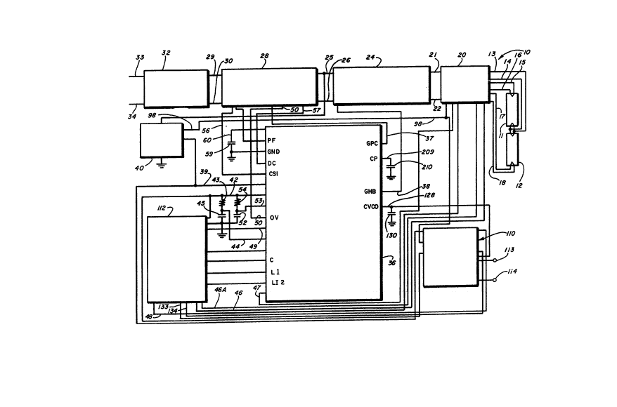
Reference numeral 110 generally designates a
dimming interface circuit which is constructed in
accordance with the principles of the invention. As shown
in Figure 1, interface circuit 110 may be connected to
control signal-applying circuitry 112 and other circuitry
of a fluorescent lamp controller which is generally
designated by reference numeral 10. The controller lO
controls the energization of two fluorescent lamps 11 and
12 in accordance with a low voltage DC control signal
applied to input terminals 113 and 114 of the interface
circuit 110. The interface circuit 110 provides high
voltage isolation between non-grounded circuits of the
controller 10 and grounded dimming controls which are
connected to the terminals 113 and 114. It converts a low
voltage DC input control signal of a standardized form to a
form which is compatible with the circuitry of the
controller 10. The interface circuit 110 is energized from
the controller 10 and it achieves safe and highly reliable
control of energization of the lamps 11 and 12.
As previously indicated, the dimmer control of the
invention is particularly designed for connection to
controllers such as disclosed in the Fellows et al.
application and which may be used for energization of
fluorescent lamps, halogen lamps or other gaseous discharge
devices or for energization of other types of loads. It
will be understood that fluorescent lamp loads are referred
to herein for ease of description and that reference herein
and in the claims to fluorescent lamps and fluorescent lamp
loads are to be construed as including all other types of
loads capable of being energized by controllers to which
the dimmer control of the invention may be connected.
The construction of the interface circuit 110 of
the invention is shown in detail in the circuit diagram of
20i~409
PHA.21-501 8 23.04.1990
Figure 4, but since the circuit 110 is particularly
designed for use with the illustrated controller 10,
certain features of the controller 10 are described before
describing the circuit 110 of Figure 4 in detail, it being
understood that the interface circuit 110 of the invention
may be used with controllers which differ from the
illustrated controller 10.
Circuits of Controller 10 (Fiaure 1~
The illustrated controller 10 is constructed in
accordance with the disclosure in the aforesaid application
Fellows et al. application V.S.Serial No. 219,923, the
complete disclosure of which is incorporated by reference.
As shown in Figure 1, the fluorescent lamps 11 and 12 are
connectable through wires 13-18 to an output circuit 20,
wires 13 and 14 being connected to one filament electrode
of lamp 11 and one filament electrode of lamp 12, wires 15
and 16 being connected to the other filament electrode of
lamp 11 and wires 17 and 18 being connected to the other
filament electrode of lamp 12. It will be understood that
the invention is not limited to use with a controller which
is usable with two lamps only.
The output circuit 20 is connected through lines 21
and 22 to the AC output of a DC-AC converter circuit 24
which is connected through lines 25 and 26 to the output
of a pre-conditioner circuit 28, the circuit 28 being
connected through lines 29 and 30 to the output of input
rectifier circuit 32 which is connected through lines 33
and 34 to a source of a 50 or 60 Hz, 120 volt RMS voltage.
In the operation of the illustrated controller 10, the pre-
conditioner circuit 28 responds to a full-wave rectified 50
or 60 Hz voltage having a peak value of 170 volts,
developed at the output of circuit 32, to supply to the DC-
AC converter circuit 24 a DC voltage having an average
magnitude of about 245 volts. The DC-AC converter circuit
24 converts the DC voltage from the pre-conditioner
circuit 28 to a square wave AC voltage which is applied to
the output circuit 20 and which has a frequency in a range
of from about 2S to 50 kHz. It will be understood that
201740~
PHA.21-501 9 23.04.1990
values of voltages, currents, frequencies and other
variables, and also the values and types of various
components, are given by way of illustrative example to
facilitate understanding of the invention, and are not to
be construed as limitations.
Both the pre-conditioner circuit 28 and the DC-AC
converter circuit 24 include SMPS (switch mode power
supply) circuitry and they are controlled by a control
circuit 36 which responds to various signals developed by
the output circuit 20 and the pre-conditioner circuit 28.
The control circuit 36 is an integrated circuit in the
illustrated controller and it includes logic and analog
circuitry which is shown in Figures 6, 7 and 8 and which is
arranged to respond to various signals applied from the
pre-conditioner and output circuits 28 and 20 to develop
and control the "GPC" and "GHB" signals on lines 37 and 39.
Figure 6 also shows the circuitry of the signal applying
circuit 112 and the connections of the dimmer circuit 110
thereto.
The pre-conditioner circuit 28 preferably has a
construction as disclosed in the aforementioned Fellows et
al. application and is a variable duty cycle up-converter.
High frequency gating pulses are applied from the control
circuit 36 through the "GPC" line 37 to a gate of the
MOSFET of the pre-conditioner circuit 28 to build-up
current through a choke and store energy therein, such
stored energy being transferred through a diode to a
capacitor in "fly-back" operations at the ends of the
gating pulses.
The DC-AC converter circuit 24 is a half-bridge
converter circuit in the illustrated controller 10 and is
supplied with a square wave gating signal "GHB" which is
applied through a line 38 from the control circuit 36. It
preferably has a construction as disclosed in the
aforementioned Fellows et al. application, and includes a
pair of MOSFETSs driven from a level shift transformer to
effect alternate conduction thereof and to develop a
square-wave output, with circuitry to protect the MOSFETs,
201740~
PHA.21-501 10 23.04.1990
shape and delay turn-on pulses and provide fast turn-offs.
In accordance with an important feature, the gating signals
"GPC" and "GHB" on lines 37 and 38 are synchronized and may
be phase shifted to avoid interference problems and to
obtain highly reliable operation. In the illustrated
controller lo, they are developed at the same frequency.
Upon initial energization of the controller 10 and
during operation thereof, an operating voltage is supplied
to the control circuit 36 through a "VSUPPLY" line 39 from
a voltage supply 40. A voltage regulator circuit within the
control circuit 36 then develops a regulated voltage on a
"VREG" line 42 which is connected to various circuits as
shown.
As shown, the "VREG" line 42 is connected through a
resistor 43 to a "START" line 44 which is connected through
a capacitor 45 to circuit ground. Following energization of
the controller 10, a voltage is developed on the "START"
line 44 which increases as a exponential function of time
and which is used for control of starting operations as
hereinafter described in detail. In a typical operation,
there is a pre-heat phase in which high frequency current
are applied to the filament electrodes of the lamps 11 and
12 without applying lamp voltages of sufficient magnitude
to ignite the lamps. The pre-heat phase is followed by an
ignition phase in which the lamp voltages are increased
gradually toward a high value until the lamps ignite, the
lamp voltages being then dropped in response to the
increased load which results from conduction of the lamps.
Important features of the controller 10 relate to
the control of lamp voltages through control of the
frequency of operation, using components in the output
circuit 20 to obtain resonance and using a range of
operating freguencies which is offset from resonance. In
the illustrated controller, the operating range is above
resonance and a voltage is developed which increases as the
frequency is decreased. For example, during the pre-heat
phase, the frequency may be on the order of 50 KHz and, in
the ignition phase, the frequency may then be gradually
2~17409
PHA.21-501 11 23.04.1990
reduced toward a resonant frequency of 36 KHz, ignition
being ordinarily obtained before the frequency is reduced
to below 40 KHz.
Upon ignition and as a result of current flow
through the lamps, the resonant frequency is reduced from a
higher no-load resonant frequency of 36 KHz to a lower
load-condition resonant frequency close to 20 KHz. ~he
operating frequency is in a relatively narrow range around
30 KHz, above the load-condition resonant frequency. It is
controlled in response to a lamp current signal which is
developed within the output circuit 20 and which is applied
to the control circuit 36 through current sense lines 46
and 46A, the line 46A being a ground reference line. When
the lamp current is decreased in response to changes in
operating conditions, the frequency is reduced toward the
lower load-condition resonant frequency to increase the
output power and oppose the decrease in lamp current.
Similarly, the frequency is increased in response to an
increase in lamp current to decrease the output power and
oppose the increase in lamp current.
As hereinafter described, the use of an operating
frequency which is above the load-condition resonant
frequency has an important advantage in providing a
capacitive load protection feature, operative to protect
against a capacitive load condition which might cause
destructive failure of transistors in the DC-AC converter
circuit 24. Additional protection is obtained through the
provision of circuitry within the output circuit 20 which
develops a signal on a "IPRIM" line 47 which corresponds to
the current in a primary winding of a transformer of the
circuit 20 and which is applied to the control circuit 36.
When the phase of the signal on line 47 is changed beyond a
safe condition, circuitry within the circuit 36 operates to
increase the frequency of gating signals on the "GHB" line
38 to a safe value, to provide additional protection of
transistors of the DC-AC converter circuit 24.
During the pre-heat and ignition phases of
operation, and also in response to lamp removal, a lamp
PHA.21-501 12 23.04.1990
voltage regulator circuit limits the maximum open circuit
voltage across the lamps, operating in response to a signal
applied through a voltage sense line 48 and to a l'VLAMP''
input line or terminal 49 of the control circuit 36,
through interface circuitry which is shown in block form in
Figure l and which is shown in detail in Figure 7 and
described hereinafter in connection therewith. The lamp
voltage regulator circuit operates to effect a re-ignition
operation in which the operating frequency is rapidly
switched to its maximum value and then gradually reduced
from its maximum value to increase the operating voltage,
to thereby make another attempt at ignition of the lamps.
The lamp ignition and re-ignition operation is
prevented in response to a drop in the output voltage of
the pre-conditioner circuit 28 below a certain value,
through a comparator within circuit 36 which is connected
through an "OV" line 50 to a voltage-divider circuit within
the pre-conditioner circuit 28, the voltage on the "OV"
line 50 being proportional to the output voltage of the
pre-conditioner circuit 28.
The designation of line 50 as an "OV" line has
reference to its connection to another comparator within
circuit 36 which responds to an over voltage on the line 50
to shut down operation of the pre-conditioner circuit 28.
Another important protective feature of the
controller relates to the provision of low supply lock-out
protection circuitry, operative to compare the voltage on
the "VSUPPLY" line 39 with the "VREG" voltage on line 42
and to prevent operation of the pre-conditioner circuit 28
and the DC-AC converter circuit 24 until after the voltage
on line 39 rises above an upper trip-point. After circuits
28 and 24 are operative, the same circuitry operates to
disable the circuits 28 and 24 when the voltage on line 39
drops below a lower trip-point. Then the DC-AC converter
circuit 24 is not allowed to be enabled until after the
voltage on line 39 exceeds the upper trip-point and a
minimum time delay has been exceeded. The required time
delay is determined by the values of a capacitor 52 which
2~17~09
PHA.21-501 13 23.04.1990
is cor.nected between a "DMAX" line 53 and ground and a
resistor 54 connected between line 53 and the "VREG" line
42.
Another feature of the controller 10 relates to the
provision of an overcurrent comparator within the circuit
36 which is connected through a "CSI" line 56 to the pre-
conditioner circuit 28 and which operates to disable
application of gating signals from the "GPC" line 37 to the
pre-conditioner circuit 28 when the current to the circuit
28 exceeds a certain value.
Additional features relate to the control of the
duration of the gating signals applied from the "GPC" line
37 to the pre-conditioner circuit 28 to maintain the output
voltage of the pre-conditioner circuit 28 at a
substantially constant average value while also controlling
the durations of the gating signals in a manner such as to
minimize harmonic components in the input current and to
obtain what may be characterized as power factor control.
In implementing such operations, the control circuit 36 is
supplied with a DC voltage on a "DC" line 57 which is
proportional to the average value of the output voltage of
the pre-conditioner circuit 28. Circuit 36 is also supplied
with a voltage on a "PF" line 58 which is proportional to
the instantaneous value of the input voltage to the pre-
conditioner circuit 28. An external capacitor 59 isconnected to the circuit 36 through a "DCOUT" line 60 and
its value has an advantageous effect on the timing of the
gating signals. It is also important for loop compensation
of the pre-conditioner control circuit 28~
Output circuit 20 of controller 10 (Figure 2)
As shown in Figure 2, the output circuit 20
comprises a transformer 64 which is preferably constructed
in accordance with the teachings in the Stupp et al. U.S.
Patent No. 4,453,109, the disclosure thereof being
incorporated by reference. As diagrammatically illustrated,
the transformer 64 comprises a core structure 66 of
magnetic material which includes a section 67 on which a
2017~
PHA.21-501 14 23.04.1990
primary winding 68 is wound and a section 69 on which
secondary windings 70-74 are wound, sections 67 and 69
having ends 67A and 69A adjacent to each other but
separated by an air gap 75 and having opposite ends 67B and
69B interconnected by a low-reluctance section 76 of the
core structure 66. In addition, although not used in a
preferred embodiment, the core structure may optionally
include a section 77 as illustrated, extending from the end
69A of the section ~9 to a point which is separated by an
air gap 78 from an intermediate point of the section 77.
After ignition, a relatively high current flowing in the
secondary windings 70-74 produces a condition in which the
resonant frequency is reduced and the "Q" is also reduced.
Secondary windings 70, 71 and 73 are filament
windings coupled to the heater electrodes through
capacitors which protect against shorting of filament
wires. Winding 72 is the lamp voltage supply winding and
winding 74 supplies the lamp voltage signal on line 48. As
shown, one end of winding 70 is connected through a
capacitor 79 to the wire 13, the other end being directly
connected to wire 14. One end of winding 71 is connected
through a capacitor 80 to the wire 15 while the other end
is directly connected to the wire 16. One end of winding 73
is connected to the wire 17 through a primary winding 81 of
a current transformer 82 while the other end of winding 73
is connected to the wire 18 through a capacitor 83 and
through a second primary winding 84 of current transformer
82. One end of winding 72 is connected to wire 16 while the
opposite end thereof is connected through a capacitor 86
to a junction point which is connected through a capacitor
87 to the wire 16, through a capacitor 88 to the wire 14
and through the winding 81 to the wire 17. The current
transformer 82 has a secondary winding 90 which is
connected in parallel with a resistor 91 and to the
current sense lines 46 and 46A.
One end of the primary winding 68 is connected
through a coupling capacitor 93 to the input line 21 while
the other end thereof is connected through a current sense
~7~
PHA.21-S01 15 23.04.1990
resistor 94 to the other input line 22 which is connected
to circuit ground. Coupling capacitor 93 operates to
remove the DC component of a square wave voltage which is
applied from the DC-AC converter circuit 24. The "IPRIM~'
line 47 is connected through a capacitor 95 to ground and
through a resistor 96 to the ungrounded end of the current
sense resistor 94. A tap on the primary winding 68 is
connected through a line 98 to the voltage supply 40, to
supply a square wave voltage of about + 20 volts for
operation of the voltage supply 40 after a start operation
as hereinafter described.
Line 98 is also connected to the dimmer circuit 110 of
the invention, to supply the same square wave operating
voltage thereto.
The output circuit operates as a resonant
circuit, having a frequency determined by the effective
leakage inductance and the secondary winding inductance and
the value of capacitor 87 which operates as a resonant
capacitor. Capacitor 87 is connected across the series
combination of the two lamps 11 and 12 and is also
connected across the secondary winding 72 through the
capacitor 86 which has a capacitance which is relatively
high as compared to that of the resonant capacitor 87 and
which operates as a anti-rectification capacitor. Capacitor
88 is a bypass capacitor to aid in starting the lamps and
has a relatively low value.
The graph of Figure 3 shows the general type of
operation obtained with an output circuit 20 such as
illustrated. Dashed line 100 indicates a no-load response
curve, showing the voltage which might theoretically be
produced across the secondary winding 72 with frequency
varied over a range of from 10 to 60 XHz, and without lamps
in the circuit. As shown, the resonant frequency in the
no-load condition is about 36 KHz and if the circuit were
operated at that frequency, an extremely high primary
current would be produced which might produce thermal
breakdowns of transistors and other components. At a
frequency of about 40 KHz, a relatively high voltage is
2017409
PHA. 21-501 16 23 . 04 .1990
produced, usually more than sufficient for lamp ignition.
Dashed line 102 indicates the voltage which would be
produced across the secondary winding 72 in a loaded
condition, with a load which is electrically equivalent to
that provided with lamps in the circuit. The resonant
frequency at the loaded condition is a substantially lower
frequency, close to 20 KHz as illustrated. The resonant
peak in the loaded condition is also of broader form and of
substantially lower magnitude due to the resistance of the
load. It should be understood that resonant peaks are shown
for explanatory purposes and that the operating range is
offset from resonance.
Actual operation is indicated by a solid line in
Figure 3. Initially, the frequency of operation is at a
relatively high value, at about 50 KHZ as illustrated and
as indicated by point 105. At this point, the voltage
across the lamps is insufficient for ignition, but a
relatively high voltage is developed across the heater
windings 70, 71 and 73. During the pre-heat phase, the
freguency is maintained at or near the point 105. Then a
pre-ignition phase is initiated in which the frequency is
gradually reduced toward the no-load resonant frequency of
36 KHZ, following the no-load response curve 100. The lamps
ll and 12 will ordinarily ignite at or before reaching a
point 106 at which the frequency is about 40 HKz and the
voltage is about 600 volts peak.
After ignition, the effective load resistance is
decreased, shifting the operation to the load condition
curve 102. In response to load current after ignition, the
frequency of operation is rapidly lowered to a point 108
which is at a frequency of about 30 KHz, substantially
greater than the loaded condition resonant peak 103.
Operation is then continued within a relatively narrow
range in the neighborhood of the point 108, being shifted
in response to operating conditions to maintain the lamp
current at a substantially constant average value.
Dimmer interface circuit (Figure 4)
2017409
PHA.21-501 17 23.04.1990
Figure 4 illustrates the dimming interface circuit
110 which is one preferred form of circuit constructed in
accordance with the principles of the invention. As afore
mentioned, the interface circuit 110 is connected to
control signal-applying circuitry 112 of the controller 10
to control the energization of the fluorescent lamps 11 and
12 in accordance with a low voltage DC control signal
applied to input terminals 113 and 114 of the interface
circuit 110. It provides high voltage isolation between
non-grounded circuits of the controller 10 and grounded
dimming controls which are connected to the terminals 113
and 114 and it converts a low voltage DC input control
signal of a standardized form to a form which is compatible
with the circuitry of the controller 10. It is energized
from the controller lo so that no separate power supply is
required.
The dimmer interface circuit 110 includes a
transformer 116 which has primary and secondary windings
117 and 118 on a core 120 of magnetic material to provide a
high coefficient of magnetic coupling therebetween. The
controller 10 provides a high frequency AC source for
energization of the primary winding 117. The upper end of
the primary winding 117 is connected through a resistor 121
to the line 98 which is connected to a tap of the primary
windings 68 of the transformer 64 of the output circuit 20,
as shown in Figure 4. As aforementioned, a square wave
voltage of about ~ 20 volts is developed at the line 98 and
is used for operation of the voltage supply 40 after
completion of a start operation. The lower end of the
primary winding 117 is connécted to ground through a level
shift circuit 122.
The secondary winding 118 is connected to a
clipping circuit 123 which operates to limit or clip the
voltage across the secondary winding to a value which is
proportional to a voltage applied to input terminals 113
and 114 and which thereby limits the voltage across the
secondary winding 118. The AC voltage across the primary
winding 117 is limited to a corresponding value as a result
~017409
PHA.21-501 18 23.04.1990
of there being a tight or high coefficient of coupling
between the primary and secondary windings 117 and 118 and
as a result of the impedance in series with the primarv
winding which is provided by the resistor 121.
The controlled AC voltage which is developed across
the primary winding 117, plus a level shift voltage
developed by the level shift circuit 122, is applied to a
peak detector and scaling circuit 124. Circuit 124 develops
a corresponding DC voltage which is used for controlling
the effective value of a resistive impedance which is
connected to the signal applying circuitry 112 and which
operates to control the controller 10 in a manner to
control energization of the lamps 11 and 12 in a manner as
hereinafter described.
To so provide a controlled resistive impedance, the
output of the peak detector and scaling circuit 124 is
connected through a line 125 to one input of a comparator
circuit 126 which has a second input connected through a
line 128 to the control circuit 36, line 128 being
connected through a capacitor 130 to ground. As hereinafter
described, the capacitor 130 is charged and discharged to
develop a periodically varying triangular voltage at the
line 128. Through comparison of the triangular voltage so
developed with the output voltage of the peak detector and
scaling circuit 124, a pulse-width-modulated square wave
signal is developed at the output of the comparator circuit
126 which has a duty cycle controlled by the voltage at
input line 125 and which is applied through an output line
131 to an analog switch circuit 132. Switch circuit 132 is
connected through a line 133 to the control circuit 36 and
through a line 134 to the signal-applying circuit 112, to
control operation of the controller 10 in a manner as
hereinafter described.
The clipping circuit 123 comprises four diodes 135-
138 which form a bridge rectifier circuit having input
terminals connected to the secondary winding 118 and having
output terminals which are connected to the collector and
emitter of a transistor 140 and also through a diode 141
'~017409
PHA.21-S01 19 23.04.1990
and a resistor 142 to circuit points 143 and 144 which are
connected through resistors 145 and 146 to the input
terminals 113 and 114. The base of transistor 140 is
connected to circuit point 144. A capacitor 147 and a Zener
diode 148 are connected between circuit points 143 and 144
and a capacitor 150 is connected between lines 113 and 114.
Zener diode 148 limits the voltage between circuit points
143 and 144 to a safe value.
In operation, a DC control voltage is applied
between the input terminals 113 and 114 which may have a
magnitude of between 1 and 10 volts, ~y way oP example. The
transistor 140 conducts to limit the output voltage of the
rectifier circuit to a value which is only slightly greater
than the control of voltage applied to the input terminals
113 and 114. It is noted that transistor 140 operates as a
current amplifier to limit the required sinking current
through the control voltage source to a relatively small
value. A control current flows from whichever terminal of
the secondary winding 118 is positive and through the
corresponding one of the diodes 135 or 136, thence through
diode 141 and resistor 145 to the terminal 113, thence
through the control voltage source to the terminal 114,
thence through the resistor 146, parallel combination of
the resistor 142 and the base-emitter junction of
transistor 140 and thence through the diode 137 or the
diode 138 to whichever of the terminals of the secondary
winding is negative. Through the amplification of the
transistor 140, a loading current flows therethrough of
sufficient magnitude to limit the peak voltage across the
secondary winding 118 to a value only slightly above the
value of the control voltage and to reliably obtain a
corresponding voltage across the primary winding for
control of lamp energization. The control current is of
very small magnitude, it flows in a direction to supply
energy to the control voltage source and it is at a minimum
when the control voltage is at a maximum. As a result,
control lines from a number of dimming interface circuits
can be connected in parallel to a common control voltage
2~ ~ 17~09
P~A.21-501 20 23.04.1990
source, when desired. Due to the transformer 116, there is
no DC path from the controller circuitry to the input
terminals and the controller circuitry is isolated from the
input terminals and voltage sources and~or the circuitry
of other controllers having interfaces connected to the
input terminals. The resistors 145 and 146, together with
capacitors 147 and 150, provide additional isolation in
providing filtering to substantially prevent transmission
to the input terminals 113 and 114 of switching noise
generated in the controller circuitry.
The bridge circuit formed by diodes 135-138
operates to transform the uni-directional DC clipping
action provided by transistor 140 into a bi-directional AC
voltage clipping action to limit the AC voltage in the
terminals of the secondary winding 118. Preferably, the
diodes 135-138 are Schottky diodes having low voltage drop
thereacross.
Since there is a tight or high coefficient of
coupling between the primary and secondary windings 117 and
118, the AC voltage across the primary winding 117
corresponds to that across the secondary winding 118.
The turns ratio of the transformer 116 may preferable be
1:1 so that the two voltages are substantially the same.
The resistor 121 has a value which is low enough to allow
development of the desired range of voltage across the
primary winding 117 while limiting current and preventing
undue loading of the AC source which is provided by the
line 98 from the controller 10.
Figure 4A shows alternative loading circuit which
includes a transformer 116A having a primary winding 117A
and having secondary winding 118A provided with a center
tap which is connectable to the emitter of transistor 140
as shown, the opposite ends of the secondary winding 118A
being connectable through two diodes 135A and 136A to the
collector of transistor 140 and also to the anode of diode
141. It will be recognized that this alternative circuit
operates in a manner similar to that of Figure 4. The
control current is amplified to apply substantially equal
2017409
PHA.21-501 21 23.04.1990
loading currents in both half cycles and to limit the
voltage across the primary winding 117A to a value
corresponding to the control voltage.
The level shift circuit 122 comprises a transistor
151 the emitter of which is connected through a protective
diode 152 to the lower end of the primary winding 117 and
the collector of which is connected to ground. A reverse
poled diode 153 is connected in parallel with the series
combination of transistor 151 and diode 152 so that current
may be conducted in both positive and negative half cycles
of the applied AC voltage. The base of the transistor 151
is connected through a resistor 154 to ground and~through
a resistor 155 to the aforementioned "VREG" line 42 at
which a regulated voltage is supplied from the control
circuit 36. Preferably, a thermistor 156 is connected in
parallel with resistor 155.
The level-shift circuit 122 operates to add a
positive DC voltage levél which is approximately egual to
the voltage at the "VREG" line 42, the transistor 151 being
operative as a buffer to limit the required current drain
on the "VREG" line 42. The provision of the thermistor 156
is important for improving the system performance,
especially at high temperatures. It is found that without
the thermistor 156, the dimming operation has a strong
temperature dependence due to cumulative effects of diode
voltage drops and that at low dim levels, lamp current can
shift as much as about 32% over a 25 Deg. C to 80 Deg. C
temperature range. In the illustrated circuit, the negative
temperature coefficient thermistor is used in conjunction
with resistors 154 and 155 to form a voltage divider
networ~ and to change the magnitude of the level shift in a
direction to offset the temperature effects of all diode
voltage drops in the dimming circuit.
The peak detector and scaling circuit 124
comprises a diode 158 the anode of which is connected to
the upper end of the primary winding 117 and the cathode of
which is connected to ground through a capacitor 160 and
through a voltage divider formed by resistors 161 and 162,
20~7409
PHA.21-501 22 23.04.1990
the output line 125 being connected to the junction of
resistors 161 and 162. During half cycles when the upper
end of the primary winding 117 is positive, the capacitor
160 is charged to a level equal to the voltage across the
primary winding 117 plus the voltage developed by the level
shift circuit 122. A certain fraction of the voltage
developed across capacitor 160 is applied to the comparator
circuit, as determined by the ratio of the resistance of
resistor 161 to the total resistance of resistors 161 and
162. It is found that for optimum performance, such
resistances should be correlated to the resistances of the
resistors 154 and 155 and the characteristics of the
thermistor 156 in the level shift circuit.
The comparator circuit 126 comprises a comparator
164 which is supplied with an operating voltage from the
"VSUPPLY" line 39. A minus input of comparator 164 is
connected through the line 128 to the control circuit 36.
A plus input is connected through a resistor 165 to the
output line 125 of the peak detector and scaling circuit
124. The output of the comparator 164 is connected to the
line 131, through a resistor 166 to its plus input and
through a resistor 167 to the "VSUPPLY" line 39.
As aforementioned, the capacitor 130 is charged
and discharged by the control circuit 36 to develop a
periodically varying triangular wave form at the line 128.
By way of example, the voltage may vary from about 2.48
volts to about 4.6 volts at a frequency of on the order of
30 KHz. The comparator 164 is triggered to an "on" state
when the voltage at its plus input, applied from the peak
detector and scaling circuit 124, is greater than the level
of the triangular wave form applied to the minus input
through the line 128. Thus, pulses are developed at the
output line 131 having durations controlled by the level of
the signal applied at the line 125. The resistor 166
provides positive feedback and hysteresis and operates to
produce cleaner noise-free output transmission from the
comparator 164 without significantly affecting the
threshold level of the comparator 164. Instead of a
20174~9
PHA.21-501 23 23.04.1990
periodically varying triangular wave form another
differently shaped periodical reference signal could be
used.
The analog switch circuit 132 comprises a
integrated circuit analog switch component 168 which is
supplied with an operating voltage from the line 39.
A resistor 170 is connected across the switch 168. By way
of example, the switch 168 may be one-fourth of a type
MC14066BCP Quad CMOS analog switch. It provides an
effective short circuit or open-circuit depending upon the
control signal it receives from the comparative circuit 126
through the line 131, a short circuit being developed from
a "high" input and an open circuit being developed from a
"low" input.
_odified Analoq Switch Circuit (Fiqure 5)
Figure 5 shows a modified analog switch circuit
132'. It comprises a MOSFET switch 171 connected between
the lines 133 and 134, in parallel with a resistor 172. The
gate of the MOSFET switch 171 is connected to the emitter
of a transistor 173 the collector of which is connected to
the supply line 39. The base of the transistor 173 is
connected through a resistor 174 to the output line 131
from the comparator circuit 126 and a diode 175 is
connected between line 131 and the gate of the MOSFET 171.
The transistor 173, operating as an emitter-follower,
converts the relatively high impedance collector output
from comparator 164 to a lower impedance, to speed up the
gate rise-time of the MOSFET 171. The diode 175 provides a
directed discharge path between the gate of the MOSFET 171
and the output of the comparator 164.
Control circuit 36 (Fiaures 6-9)
Circuitry within the control circuit 36 and
associated external components are shown in Figures 6,7 and
8. Figure 6 shows pulse width oscillator and oscillator
circuitry for producing the "GCP" and "GHB" gating signals
on lines 37 and 38; Figure 7 shows circuitry for applying
20~7409
PHA~21-501 24 23.04.1990
variable frequency and control signals to the oscillator
circuitry shown in figure 6, also showing the signal-
applying circuitry 112 shown in block form in Figure l;
and Figure 8 shows circuitry for applying control signals
to the pulse width modulator circuitry shown in figure 6.
figure 9 is a graph illustrating the waveforms produced in
phase comparison circuitry shown in figure 7, for
explanation of the operation thereof.
Pulse width modulator and oscillator circuitry (Fiaure 6)
As shown in Figure 6, the "GPC" and "GHB" lines 37
and 38 are connected through the outputs of "PC" and "HB"
buffers 191 and 192 of the control circuit 36. The input of
the "PC" buffer 191 is connected to the output of an AND
gate 193 which has three inputs including one which is
connected to the output of a "PC" flip-flop 194 operative
for controlling the generating of pulse width modulated
pulses. The input of the "HB" buffer 192 is connected to
the output of a comparator 195 having inputs connected to
the two outputs of a "HB" flip-flop 196 which is controlled
to operate as an oscillator and generate a square-wave
signal.
Circuits used for the "HB" oscillator flip-flop 196
are described first since they also control the time at
which the "PC" flip-flop 194 is set in each cycle, reset of
the "PC" flip-flop 194 being performed by other circuits to
control the pulse width. As shown, the set input of the
"HB" flip-flop 196 is connected to the output of a
comparator 197 which has a plus input connected through a
"CVCO" line 198 to an external capacitor 200. The minus
input of comparator 197 is connected to a resistance
voltage divider, not shown, which supplies a voltage equal
to a certain fraction of the regulated voltage "VREG" on
the line 42, a fraction of 5/7 being indicated in the
drawing. The reset input of the "HB" flip-flop 196 is
connected to the output of an OR gate 201 which has one
input connected to the output of a second comparator 202.
The minus input of comparator 202 is connected to the
~0~74~
PHA.21-501 25 23.04.1990
"CVCO" line 198, while the plus input thereof is connected
to a voltage divider which supplies a voltage equal to a
certain fraction of the "VREG" voltage, less than that
applied to the minus input of comparator 197, a fraction of
3/7 being indicated in the drawing.
The "CVCO" line 198 is connected through a current
source 204 to ground. Current source 204 is bi-directional
and controlled through a stage 205 from the output of the
"HB" flip-flop 196 to charge the capacitor 200 at a certain
rate when the "HB" flip-flop 196 is reset and discharge the
capacitor 200 at the same rate when the "HB" flip-flop 196
is set. The rate of charge and discharge is the same and is
maintained at a constant rate which is adjustable under
control by a control signal on an "FCONTROL" line 206.
In the operation of the "HB" oscillator circuit as
thus far described, the capacitor 200 is charged through
the source 204 until the voltage reaches the upper level
set by the reference voltage applied to comparator 197 at
which time the flip-flop 196 is set to switch the source
204 to a discharge mode. The capacitor 200 is then
discharged until the voltage reaches the lower level set by
the reference voltage applied to comparator 202 at which
time the flip-flop 196 is again reset to initiate another
cycle. The frequency is controlled by the charge and
discharge rate which is controlled by the control signal on
the "FCONTROL" line 206.
In the pulse width modulator circuitry, a current
source 208 is provided which is connected between ground
and a "CP" line 209 to an external capacitor 210 and which
is also controlled by the signal on the "FCONTROL" line
206, current source 208 being operative only in a charge
mode. A solid state switch 211 is connected across
capacitor 210 and is closed when the flip-flop 194 is
reset. When a signal is developed at the output of
comparator 202 to reset the "HB" flip-flop 196, it is also
applied to the set input of the "PC" flip-flop 194 which
then operates to open the switch 211 and to allow charging
of the capacitor 210 at the constant rate set by the
2~7~09
PHA.21-501 26 23.04.1990
control signal on the "FCONTROL" line 206.
In normal operation, charging of the capacitor 210
continues until its voltage reaches the level of signal on
a "DCOUT~' line 60 which is developed by other circuitry
within the circuit 36 as hereinafter described in
connection with Figure 8.
The "DCOUT" signal on line 60 is applied to the
minus input of a comparator 214, the plus input of which is
connected to the "CP" line 209. The output of the
comparator 214 is applied through an OR gate 215 and
another OR gate 216 to the reset input of the "PC" flip-
flop 194 which operates to close the switch 211 and to
discharge the capacitor 210 and place the line 209 at
ground potential. The line 209 remains at ground potential
until the flip-flop 194 is again set in response to a
signal from the output of the comparator 202.
The "PC" flip-flop 194 may also be reset in
response to any one of three other events or conditions.
The second input of the OR gate 216 is connected to a
"PWMOFF" line 217 which is connected to other circuitry
within the control circuit 36, as described hereinafter in
connection with Figure 8. The second input of the OR gate
215 is connected to the output of a comparator 218 which
has a plus input connected to the "CP" line 209 and which
has a minus input connected to a resistance voltage
divider, not shown, which supplies a voltage equal to a
certain fraction of the regulated voltage "VREG" on the
line 42, a fraction of 9/14 being indicated in the drawing.
If, at any time after the flip-flop 194 is set, the voltage
on line 209 exceeds the reference voltage applied to the
minus input of comparator 218, the flip-flop 194 will be
reset. Thus, there is an upper limit on the width of the
generated pulse.
A third input of the OR gate 215 is connected to
the output of a comparator 220 which has a plus input
connected to the line 209 and a minus input connected to
the aforementioned "DMAX" line 53. The "DMAX" line 53 is
also connected to other circuitry within the control
2017~9
PHA.21-501 27 23.04.1990
circuit 36 and the operation in connection with the "DMAX"
line 53 is described hereinafter.
Provisions are made for disabling both the half
bridge oscillator and pulse width modulator circuits in
response to a signal on a "HBOFF" line 222 which is
connected to solid state switches 223 and 224 operative to
connect the "CVCO" and "CP" lines 198 and 209 to ground.
Line 222 is also connected to a second input of the OR gate
201 to reset the "HB" flip-flop 196. An inverter circuit
225 is connected between the set input of flip-flop 194 and
an input of the AND gate 193. Another inverter 226 is
connected between the output of the OR gate 215 and a third
input of the AND gate 193, for the purpose of insuring
development of an output from the pulse width modulator
circuit only under the appropriate conditions.
FrequencY control and siqnal-a~Dlyinq circuitry (Fiqure 7)
Figure 7 shows frequency control circuitry which is
incorporated within the control circuit 36 and also shows
the signal-applying circuitry 112 to which the dimming
interface circuit 110 of the invention is connected. The
frequency control circuitry of Figure 7 operates to control
the level of the fre~uency control signal on the "FCONTROL"
line 206 which is applied to the current sources 204 and
208 of the oscillator and pulse-width modulator circuitry
of Figure 6. As shown in Figure 7, line 206 is connected to
the output of a summing circuit 228 which has inputs
connected to two current sources 229 and 230. The current
source 229 is controlled in conjunction with starting
operations and in conjunction with "retry" operations made
when the lamps fail to ignite a starting operation. The
current source 230 is controlled in response to output lamp
current.
In normal operation, after ignition, the current of
the current source 229 is constant, changes in frequency
being controlled solely by the current source 230. Current
source 230 is connected to the output of a lamp current
error amplifier 231 which has a minus input supplied with a
2~7409
PHA.21-501 28 23.04.1990
reference voltage developed by voltage divider (not shown)
within the circuit 36, a reference voltage of 2/7 of the
regulated voltage "VREG" being indicated.
The plus input of the amplifier 231 is connected to
a "CRECT" line 232 which is connected through the signal-
applying circuit 112 to one output line 133 of the dimming
interface circuit 110 of the invention. The plus input of
amplifier 231 is also connected through a current source
- 234 to ground. Current source 234 is controlled by an
active rectifier 236 having inputs which are connected
through "LI" and lines 237 and 238 and external resistors
239 and 240 to the current sense lines 46 and 46A. As
shown, the current sense line 46A is a ground interconnect
line.
In the signal-applying circuitry 112, the "CRECT"
line 232 is connected through a capacitor 241 to ground and
also to the output line 134 from the dimming interface
circuit 110 of the invention. The second output line 133 of
the dimming interface circuit 110 is connected through a
resistor 242 to ground and is also connected through a
resistor 243 to a circuit point 244 which is connected
through a resistor 245 to ground and through resistors 246
and 247 to a circuit point 248. Circuit point 248 is
connected through a diode 250 to the voltage sense line 48,
through a capacitor 251 to ground and also through a pair
of resistors 253 and 254 to ground, the "VLAMP" line 49
being connected to the junction between resistors 253 and
254. A diode 256 is connected between the junction between
resistors 246 and 247 and the l'VREG" line 42 to limit the
voltage at that junction to the regulated voltage on line
42.
In operation, amplifier 231 is controlled by
summation of a first control signal applied from the
current source 234 and a second control signal applied from
the "CRECT" line 232. The amplifier 231, in turn, controls
the current source 230 which operates through the summing
circuit 228 and line 206 to control the current source 204
(Figure 6) and thereby control the frequency of operation.
2~17409
PHA.21-501 29 23.04.1990
The first control signal, which is applied from the
current source 234, is controlled by the active rectifier
236 to be controlled in accordance with the lamp current
which is sensed by the current transformer 82. The lamp
current is thereby regulated at a value which is dependent
upon the second signal which is from the dimming interface
circuit 110 of the invention. In particular, the dimming
interface circuit 110 controls the effective resistance
between the "CRECT" line 232 and the junction between
resistors 242 and 243 and thereby controls the signal
applied through the line 232 to the lamp correction error
amplifier 231. Operation is thereby controlled in
accordance with the control signal applied to the input
terminals 113 and 114 of the dimming circuit 110. The diode
256 serves to limit the voltage developed at the "CRECT"
line during start-up. The values of the resistors 242, 243,
245, 246 and 247 are determined by the characteristics of
the lamps and other components and may be changed for
different ratings or types of lamps.
To establish a minimum frequency of operation, a
control current is applied to the current source 229
through a "FMIN" line 257 which is connected through a
resistor 257A to a circuit point which is connected through
a resistor 258 to ground and through a pair of resistors
259 and 259A to the "VREG" line 42.
The current source 229 is also controlled by a
"frequency sweep" amplifier 260 which has a plus input
connected to a reference voltage source, a reference of 4/7
of the regulated voltage on line 42 being shown. The minus
input of amplifier 260 is connected to the "START" line 44
and is also connected through two switches 261 and 262 to
ground. Switch 261 is controlled by a comparator 263 to be
closed when the output voltage of the pre-conditioner
circuit 28 is less than a certain threshold value. As
shown, a reference voltage of 5/7 of the regulated voltage
on line 42 is applied to its plus input and its minus input
is connected to the "OV" line 50.
The switch 262 is connected to an output of a
2017~09
PHA.21-501 30 23.04.1990
~'VLAMP OFF" flip-flop 264 which has a reset input connected
to the output of a "START" comparator 265. The minus input
of comparator 265 is connected to the "START" line 44 and
the plus input thereof is connected to a reference voltage
source, a reference of 3/14 of the regulated voltage on
line 42 being indicated. The set input of the flip-flop
264 is connected to the output of an OR gate 266 which has
inputs for receiving any one of three signals which can
operate to set the "VLAMP OFF" flip-flop and to cause
closure of the switch 262.
One input of OR gate 266 is connected to the output
of a lamp voltage comparator 267, the minus input of
comparator 267 being connected to the "VREG" line 42 and
the plus input thereof being connected to the "VLAMP" line
49. When the lamp voltage exceeds a certain value, a signal
is applied from the lamp voltage comparator 267 to set the
flip-flop 264 and to thereby effect closure of the switch
262 and grounding of the "START" line 44.
A second input of OR gate 266 is connected to be
responsive to setting of a flip-flop of pulse width
modulator circuitry shown in Figure 8 and described
hereinafter.
A third input of OR gate 266 is connected to be
responsive to a signal which is generated by circuitry
described hereinafter, to effect operation of the flip-flop
264 when the phase of the signal on the "IPRIM" is changed
beyond a safe value.
In the start operation, the current of the current
source 229 has a maximum value and the current of source
230 has a minimum value and the frequency is at a certain
maximum value, such as 50 KHz. The voltage applied by the
output circuit, once the pre-conditioner and DC-AC
converter circuits 28 and 24 are operative, is sufficient
for heating the lamp filaments but insufficient for
ignition of the lamps. When power is initially supplied to
the controller 10, the switch 261 is closed and the switch
262 is open. After the voltage on the "OV" line 50 exceeds
5/7 (VREG), the switch 261 is opened by the low HB voltage
2017409
PHA.21-501 31 23.04.1990
comparator 263. Then the voltage of the "START" line 44
will start to rise exponentially in response to current
flow through the resistor 43.
When the voltage of the "START" line 44 approaches
a certain level, determined by the reference voltage
applied to the frequency sweep amplifier 260, at around 4/7
("VR~G"), the ignition phase is initiated. At this time,
the frequency sweep amplifier 260 starts to decrease the
current through the current source 229 to operate through
the summing circuit 228 and the line 206 to decrease the
frequency of operation. When the frequency is decreased to
a certain value, the lamps will ignite, usually at a
frequency above 40 KHz. The lamp operation phase is then
initiated. At this time, the effective resonant frequency
of the output circuit is lowered substantially. At the same
time, the current through the lamps is sensed by the
current transformer 82 and a control signal is developed by
the active rectifier 236 to operate to drop the frequency
to a range appropriate for operation of the lamps, at
around 30 K~z.
If the lamps should fail to ignite during the
ignition phase, the frequency will continue to be lowered
and the lamp voltage will continue to increase until
voltage on the "VLAMP" line 49 reaches a certain value, at
which time the lamp voltage comparator 267 will apply a
signal through the OR gate 266 to set the flip-flop 264 and
to effect momentary closure of the switch 262 to ground the
"START" line 44 and discharge the capacitor 45. The voltage
of "START" line 44 is then dropped below a certain value
and a reset signal is applied from the start comparator 265
to reset the flip-flop 264. Then the voltage of the "START"
line will again start to rise exponentially. When it
reaches a certain higher value, the ignition phase is again
initiated through operation of the frequency sweep
comparator 260 in the manner as above described. Thus one
or more "retry" operations are effected, continuing until
ignition is obtained, or until energization of the
controller is discontinued.
2~17409
PHA.21-501 32 23.04.1990
As aforementioned, the flip-flop 264 may also be
operated to a set condition when the phase of the signal on
the "IPRIM" line changes beyond a safe value. The circuitry
shown in Figure 7 further includes a primary current
comparator 268 having a minus input connected to the
"IPRIM" line 47 and having a plus input connected to a
source of reference voltage, which is not shown but which
may supply a reference voltage of -0.1 volts as indicated.
The output of the comparator 268 is connected to one input
of an AND gate 269 and is also connected to one input of a
NOR gate 270. The output of the AND gate 269 is connected
to the reset input of a "CLP" flip-flop 272 having an
output connected to a second input of the NOR gate 270. The
set input of the flip-flop 272 is connected to the output
of an inverter 273. The input of the inverter 273 and a
second input of the AND gate 269 are connected together
through a line 274 to the half bridge oscillator circuitry
shown in Figure 6, being connected to the output of the
half bridge flip-flop 196. The output of the NOR gate 270
is connected through the OR gate 266 to the set input of
the flip-flop 264.
In operation, the output of the NOR gate 270 is
high only when the flip-flop 272 is reset and, at the same
time, the output of the primary current comparator 268 is
low. Such conditions can take place only when the phase of
the current on the line 47 relative to the signal applied
on the line 274 is changed in a leading direction beyond a
certain threshold angle which is determined by the
reference voltage applied to the primary current comparator
268. The signal on line 274 is supplied from the output of
the "HB" flip-flop 196 (Figure 6) which supplies the gating
signals to the DC-AC or half bridge convertor circuit 24.
Figure 9 is a graph which shows the relationship of
the voltages on line 274 and at the outputs of comparator
3S 268, flip-flop 272 and NOR gate 270 as the phase of the
signal on the "IPRIM" line is advanced in a leading
direction. When the trailing edge of the output of
comparator 268 occurs before the leading edge of the output
20174~9
PHA.21-501 33 Z3.04.1990
of flip-flop 272, the output of NOR gate 270 goes high and
is applied through the OR gate 266 to set the "VLAMP'"'
flip-flop 264, and to cause the frequency to sweep hiqh in
the manner as described above.
The circuitry shown in Figure 7, including
components 268, 269, 270, 272 and 273, is operative in the
arrangement as shown for checking only the conduction of
one of the MOSFETS of the circuit 24. Normally, it will
provide more than adequate protection with respect to the
other MOSFET, using the circuitry as shown and described.
However, it will be understood that for additional
protection or with other types of converter circuits, a
phase comparison arrangement as shown may be provided for
each other MOSFET or other type of transistor of the
converter.
Pulse Width Modulator Control Circuitry (Fia. 8)
The voltage on the "DCOUT" line 60, which controls
the width of the pulses generated by the pulse width
modulator circuit of Figure 8, is developed at the output
of a multiplier circuit 276 which has one input connected
to ground through a current source 277 which is controlled
by a DC error amplifier 278. The plus input of the
amplifier 278 is connected to the voltage regulator line
42 while the minus input thereof is connected to the "DC"
line 57 on which a voltage is applied proportional to the
output voltage of the pre-conditioner circuit 28. The other
input of the multiplier circuit 276 is connected to the
output of a summing circuit 280 which is connected to two
current sources 281 and 282.
Current source 281 supplies a constant reference or
bias current in one direction while current source 282
supplies a current in the opposite direction under control
of the voltage on the "PF" line 58. The source 282 is
connected to the output of a "PF" amplifier 282 which has
a plus input connected to line 58 and a minus input
connected to ground. In operation, the input waveform is,
in effect, inverted through control of the current source
2017409
PHA.21-501 34 23.04.1990
282 and then added to a reference determined by the current
source 281, the waveform being multiplied by a value
proportional to the average output of the preconditioner
circuit 28.
With proper adjustment, a control of the width of
each gating pulse is obtained such that the average input
current flow during the short duration of each complete
gating pulse cycle is proportional to the instantaneous
value of the input voltage to the pre-conditioner circuit.
At the same time, the pulse widths are controlled through
the current source 277 to control the total energy
transferred in response to all of the high frequency gating
pulses applied during each complete half cycle of the
applied full wave rectified low freguency 50 or 60 Hz
voltage. The result is that the output voltage of the pre-
conditioner circuit 28 is substantially constant while at
the same time, the input current waveform is proportional
to and in phase with the input voltage waveform, so that
the input current waveform is sinusoidal when the input
voltage waveform is sinusoidal.
The PWMOFF" line 217 is connected to the output of
an OR gate 286 which has one input connected to the output
of an over-current comparator 287. The plus input of
comparator 287 is connected to a reference voltage source
(not shown) which may supply a voltage of -0.5 volts, as
indicated. The minus input of the comparator 287 is
connected to the "CSl" line 56. In operation, if the input
current to the pre-conditioner circuit 28 should exceed a
certain level, the over-current comparator 287 applies a
signal to the OR gate 286 to the line 217 and through the
OR gate 216 to reset the pre-conditioner flip-flop 194
(see Fig. 6).
A second input of the OR gate 286 is connected to
an output of a "PWM OFF" flip-flop 288 which has a set
input connected to the output of a Schmitt trigger circuit
289 having one input connected to the "VSUPPLY" line 39 and
having a second input connected to the voltage regulator
line 42. As shown, a voltage regulator 290 is incorporated
20~7409
PHA.21-501 35 23.04.1990
in the control circuit 36 and is supplied with the voltage
on line 39 to develop the regulated voltage on line 42. The
output of the Schmitt trigger circuit 289 is also applied
to the set input of a flip-flop 292 which is connected to
the "HBOFF" line 22. In operation, if the supply voltage
should drop below a certain level, both flip-flops 288 and
292 are set to disable the pulse width modulator and half
bridge oscillator circuits.
The reset input of the flip-flop 292 is connected
to the output of a "DMAX" comparator 294 which has a plus
input connected to the "DMAX" line 53, the minus input of
the comparator 294 being connected to a source of a
reference voltage which may be 1/7 ("VREG") as indicated.
The reset input of the flip-flop 288 is connected to the
output of an inverter 295 which has an input connected to
the output of the comparator 294. The "DMAX" line 53 is
also connected through a switch 296 to ground, switch 296
being controlled by the "PWM OFF" flip-flop 288.
It is noted that the output of the flip-flop 288 is
also connected through a line 297 to a third input of the
OR gate 266 in the frequency control circuitry shown in
Figure 7. An overvoltage comparator 300 has an input
connected to the "OV" line 50 and an output connected
through the OR gate 256 to the "PWM OFF" line 217.
In the operation of the pulse width modulator
control circuitry of Figure 8, the flip-flops 288 and 292
are, of course, in a reset condition when the controller is
initially energized. After a certain time delay, as
required for the voltage on the "VSUPPLY" and "VREG" lines
3~ 39 and 42 to develop, the Schmitt trigger circuit operates
to set both flip-flops 288 and 292 but thereafter, the
flip-flop 288 is re~et through the inverter 295 from the
output of the "DMAX" comparator 294. Then, when the "DMAX"
comparator 52 is charged to a value greater than 1/7
(VREG), the "DMAX" comparator operates to reset the "HBOFF"
flip-flop 292. At this time, operation of the "HB"
oscillator flip-flop 196 (Figure 6) may commence. The
operation of the "PC" flip-flop 194 (Figure 6) may also
2~l7~a~
PHA.21-501 36 23.04.1990
commen~e. Initially the width of the "GPC" gate pulses are
controlled by the increasing signal on the "DMAX" line 53
so that the output of the pre-conditioner circuit 28
gradually increases and thus, a "soft" start is obtained.
The "DMAX" voltage thus controls a time delay in
turning on the oscillator circuitry after initial
energization and thereafter controls the width of pulses
generated by the pulse width modulator flip-flop 194, so as
to obtain the gradually increasing voltage and the "soft"
start.
The illustrated construction of the dimming
interface circuit is particulary advantageous in that it is
readily connected to and usable with the controller 10 as
disclosed which provides dynamic controls to automatically
respond to variations in operating conditions and in the
values or characteristics of components in a manner such as
to obtain safe and reliable operation while at the same
time achieving optimum performance and efficiency. for
example, the dimmer circuit is operative over a wide range
of frequencies such as developed during operation the
controller 10 which is so operated as to allow for
substantial variations in the resonant freguency in the
output circuit. The clipping circuit provides tight control
of the voltage across the secondary winding and with the
tight magnetic coupling of the primary and secondary
windings and the direct detection of the voltage across the
primary winding, the relationship of the dimmer circuit
output to its input is substantially independent of
frequency over a wide range.
Modified Circuit With On/Off Control (Fiqure 10)
Figure 10 shows a modified dimming interface
circuit 302 which is constructed in accordance with the
principles of the invention and which is operative to
provide an "OFF" function. The circuit 302 includes the
transformer 116, level shift circuit 122, clipping circuit
123, peak detector and scaling circuit 124, comparator
circuit 126 and analog switch circuit 132 of the circuit
2~74~9
PHA.21-501 37 23.04.1990
shown in Figure 4. In addition, it includes an on/off
circuit 304 having output terminal 305 and 306 which are
connected to the "FMIN" line 257 and the "START" line 44.
The output terminal 305 is connected through a resistor
307, a diode 30~ and a analog switch 310 to the "VREG" line
42. The output terminal 306 is connected through a second
analog switch 312 to ground.
Analog switches 310 and 312 are controlled from an
output of comparator 314 which has a minus input connected
to the output line 125 of the peak detector and scaling
circuit 124. The plus input of comparator 314 is connected
through a resistor 315 to the "VREG" line 42, through a
resistor 316 to ground and through a resistor 317 to the
output of the comparator 314 which is also connected
through a resistor 318 to the "VSUPPLY" line 39.
In operation, the output of the peak detector and
scaling circuit 124 is sensed at the minus input of the
comparator 314 and when it equals a reference voltage
applied to the plus input, the output of comparator 314
switches from a "low" state to a "high" state, to
simultaneously switch the two analog switches 310 and 312
to an "on" or closed condition. The switch 312 operates to
discharge the capacitor 45 which is connected to the
"START" line 44 while the analog switch 310 injects a
calibrated DC current into the "FMIN" input of the control
circuit 36. The calibrated DC current is determined by the
value of resistor 307 and causes the controller circuit to
operate at a frequency which is well above the preheat
frequency. In this high frequency state, the frequency of
operation is very far away from resonance and no
significant power is delivered to the lamp load, including
the filaments. The lamps are the extinguished and a low
power "OFF" condition results, but the lamps can be quickly
reenergized by increasing the control voltage applied to
the input terminals. Hysteresis from positive feedback
resistor 317 insures clean transitions.
It will be understood that modifications and
variations may be effected without departing from the
~017409
PHA.21-501 38 23.04.1990
spirit and scope of the novel concepts of this invention.