Note: Descriptions are shown in the official language in which they were submitted.
~~~~~a _~
-1- LD 9949
OPTICAL INTERFERENCE COATINGS AND LAMPS USING SAME
BACKGROUND OF THE INVENTION
Field of the Invention
This invention relates to thin layer optical
S interference coatings for reflecting infrared radiation
and transmitting visible light radiation and their use
on lamps. More particularly, this invention relates to
optical interference coatings made of alternating high
and low refractive index layers for reflecting infrared
radiation and transmitting visible light radiation
which comprise three spectrally adjacent multiperi~d
stacks with the first stack being a conventional short
wave pass stack having at least two periods and with
the second and third stacks each comprising at least
two periods and being spectrally located at
increasingly longer wavelengths than the first stack,
and lamps containing such filters.
Background of the Disclosure
Thin film optical interference coatings known as
interference filters which comprise alternating layers
of two or more materials of different refractive index
are well known to those skilled in the art. Such
~~~~~~i ~~~.
-2- LD 9949
coatings or films are used to selectively reflect
and/or transmit light radiation from various portions
of the electromagnetic spectrum such as ultraviolet,
visible and infrared radiation. These films or
coatings are used in the lamp industry to coat
reflectors and lamp envelopes. One application in
which these thin film optical coatings have been found
to be useful is to improve the illumination efficiency
or efficacy of incandescent and arc lamps by
reflecting infrared radiation emitted by a filament or
arc back to the filament or arc while transmitting the
visible light portion of the electromagnetic spectrum
emitted by the filament or arc. This lowers the
amount of electrical energy required to be supplied to
the filament or arc to maintain its operating
temperature. In other lamp applications where it is
desired to transmit infrared radiation, such filters
can reflect the shorter wavelength portions of the
spectrum, such as ultraviolet and visible light
portions emitted by a filament or arc and transmit
primarily the infrared portion in order to provide
heat radiation with little or no visible light
radiation. Such an application of this latter type
would include a typical radiant heater for residential
or industrial use where visible radiation emitted by
the heater is unwanted.
Optical interference coatings or filters used for
applications where the filter will be exposed to high
temperatures in excess of 500'C or so have been made
of alternating layers of refractory metal oxides such
as tantala (tantalum pentoxide Ta~05), titania
(titanium dioxide Ti02), niobia (niobium pentoxide,
Nb205) and silica (Si02), wherein the silica is
the low refractive index material and the tantala,
-3' LD 9949
titanic or niobia is the high refractive index
material. Such filters and lamps employing same are
disclosed, for example, in U.S. Patents 4,588,923;
4,663,557 4,689,519 and 4,734,614. In such lamp
applications, the filters are applied on the outside
surface of the vitreous lamp envelope containing the
filament or arc within and often reach operating
temperatures as high as 900'C. These interference
filters or coatings are applied using evaporation or
sputtering techniques and also by chemical vapor
deposition (CVD) and low pressure chemical vapor
deposition (LPCVD) processes. Some attempts to make
such interference filters have employed solution
deposition techniques such as is disclosed in U.S.
Patent 4,701,663. Solution deposition techniques
however produce relatively thick layers which tend to
crack and which severely limits the filter design.
CVD and particularly LPCVD deposition processes are
preferred for applying coatings to other than flat
objects such as reflectors and lamps.
SUI~fARY OF THE I .NTTQj~J
The present invention relates to an optical
interference coating for reflecting infrared radiation
and transmitting visible light radiation which
comprises a plurality of alternating high and low
refractive index layers and has a spectrally broad
high transmittance of an average of at least about 90%
between about 400 to 770 nm and a spectrally broad
high reflectance of an average of at least about 70%
between about 800 to 1900 nm. In a preferred
embodiment these filters comprise three multiperiod,
spectrally adjacent stacks with all three of the
stacks having at least two periods wherein one of the
stacks is a conventional short wave pass stack and
~~ _~ ,~ r~. ''~ 3.
-4- LD 9949
wherein the other two stacks .are spectrally located at
wavelengths different from each other and longer than
the wavelength of the short wave pass stack.
The filter of the present invention will
preferably be the result of a computer optimization of
a filter design comprising three spectrally adjacent
multiperiod stacks with said first stack being a
conventional short wave pass stack having at least two
periods and with said second and third stacks being
spectrally located at wavelengths different from each
other and longer than the wavelength of the first
stack and comprising at least two periods for each
stack, with each period of said second and third
stacks containing seven alternating layers of high and
low refractive index materials of the form:
~~r #i
a b c d c b a
wherein 2 < a < 4
5 << b < 15
5 << c < 15
1 < d < 2.5
and wherein L and H represent the low and high index
of refraction materials, respectively, L and H each
being defined as having an optical thickness of a
quarterwave of the stack wavelength. Accordingly, the
notation a represents a fraction of a quarterwave
of optical thickness of the L material at the stack
wavelength, i.e., one-half of a quarterwave (1/8 wave)
for a = 2. The very thin layers b and ~ have an
optical thickness no greater than one-twentieth of the
stack wavelength and serve to frustrate the higher
order reflectance bands of the stack which would
interfere with light transmittance in the visual
spectral region. The optical thickness of the other
-5- LD 9949
layers of these periods will be nearly equal to, but
less than those which would be found in a conventional
short wave pass stack of the game stack wavelength.
As set forth above, the filters of the present
invention provide a spectrally broad high
transmittance region across the visible spectrum of at
least about 90% average between about 400-770 nm and a
spectrally broad high reflectance region of at least
about 70% average across the near infrared spectrum
between about 800-1900 nm. These coatings have been
found to be particularly useful on the vitreous
envelopes of lamps for increasing the efficiency and
efficacy of the lamp for visible light transmission by
reflecting the infrared radiation back to the filament
or arc to increase the efficacy of the lamp.
In a particularly preferred embodiment the first
stack is the outermost stack which interfaces with the
atmosphere (ambient) and is the shortest wavelength
stack, being a conventional short wave pass
quarterwave stack having at least two and preferably
at the least three periods of alternating high and low
refractive index layers comprising a high refractive
index central layer having an optical thickness of
about a quarter of the stack wavelength with a low
refractive index layer adjacent both sides of the
central layer and with said low refractive index
layers each having an optical thickness of about an
eighth of the stack wavelength.
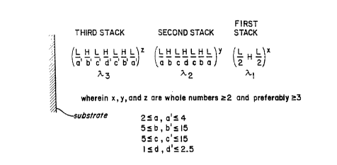
HRIEF DESCRTpTTnN nF msr~ n~ae,ray~e
Figure 1 is a graphic representation of the filter
according to the present invention illustrating the
stacks and the periods in the stacks.
'6- LD 9949
Figure 2 is a graphic representation of an actual
filter design according to the present invention
wherein the optical thickness of each layer has a
definite value.
Figure 3 illustrates the theoretical spectral
transmittance of a filter of the present invention and
a conventional prior art filter designed for infrared
reflectance and visible light transmittance.
Figure 4 illustrates the actual spectral
transmittance of a filter of the present invention for
infrared reflectance and visible light transmittance.
Figure 5 schematically illustrates an elongated
double ended tungsten halogen lamp having an infrared
reflecting light interference film according to the
present invention on the outer surface of the lamp
envelope.
Figure 6 schematically illustrates a small double
ended tungsten halogen lamp having an infrared
reflecting film of the present invention on the outer
surface of the vitreous lamp envelope.
Figure 7 schematically illustrates the tungsten
halogen lamp of Figure 6 mounted in a parabolic
reflector.
D~TATLD DESCRTPTTON
The invention relates to the use of thin coating
layers in a multilayer coating design to achieve what
is called hot mirror performance for reflecting
infrared radiation and transmitting visible light
. ~!. '..' to
-~- LD 9949
radiation. If one attempts to make interference
filter hot mirror coatings comprising alternating
layers of two different materials having high and low
indices of refraction at conventional layer thickness
of, i.e., about 1000 A or more, the width of the
visual window in transmission is primarily determined
by the refractive index ratio of the coating
materials. Since the selection of suitable materials
can be limited due to temperature and other
considerations, the width of the visible transmission
window can also be limited. In the case of infrared
reflective coatings for lamp envelopes, temperature
considerations tend to limit the materials which can
be used for the coating. One approach to widening the
visual transmission window would be to use three
coating materials, with the third material having an
index of refraction somewhere in between the high and
low index materials, with the necessary intermediate
index of refraction being determined by the index of
refraction of the other two materials. Although this
will work for lamp applications, the three material
approach is limited by the availability of suitable
coating materials having the necessary refractive
indices, physical and chemical compatibility and by
the stress buildup occurring in a coating from using
three different materials having three different
coefficients of thermal expansion.
By using thin layers according to the present
invention, one can obtain a filter that provides a
spectrally broad, high transmittance region across the
visible spectrum and a spectrally broad, high
reflectance region across the near infrared portion of
the spectrum. By thin layers is meant at least some
of the layers in the second and third stacks have an
optical thickness no greater than one-fifth of a
~~~. e~l~r~~
-8- LD 9949
quarterwave of the stack wavelength or no greater than
one-twentieth of the stack wavelength. A performance
similar to employing three different materials can be
achieved using only two materials in filters according
to the present invention.
A thin layer interference filter optical coating
also provides less sensitivity to layer thickness
errors. If a systematic optical thickness error
occurs such that all the layers are either too thick
or too thin, the effect will be a shift in the
transmission window in the visible wavelength to a
longer or a shorter wavelength, respectively. A wider
window will allow for a larger shift before the
apparent color of the lamp employing the filter is
changed. The greater tolerance to layer thickness
variation in the coating of the present invention also
provides more leeway with respect to both mismatch
errors and random errors. Mismatch errors are defined
as coating process systematic errors which produce a
final coating in which the optical thickness of all
the layers of one material is thicker than desired and
the optical thickness of all the layers of the other
material is thinner than desired. This type of error
does not shift the location of the visible window, but
does degrade the high transmittance level and observed
color. Random errors are errors in coating layer
thickness which occur randomly as a result of normal
imperfections in manufacturing process control. This
error type also degrades transmittance and observed
color. Using a thin layer filter according to the
present invention provides a significant advantage in
increased load sizes, less costly deposition control
systems and higher product yield.
When a lamp employing conventional IR reflecting
~, -~ t ;r R
;~.' ~ t4~
'9- LD 9949
coatings or filters is viewed at angles other than
normal to the surface, the observed effect is a
spectral shift in the window location to shorter
wavelengths which make the lamp appear blue or
blue-green. The wider window of the coating of this
invention provides a larger allowable viewing angle
off normal before color change is observed.
As set forth above, The present invention relates
to an optical interference coating for reflecting
infrared radiation and transmitting visible light
radiation which comprises a plurality of alternating
high and low refractive index layers and has a
spectrally broad high transmittance of an average of
at least about 90% between about 400 to 770 nm and a
spectrally broad high reflectance of an average of at
least about 70% between about 800 to 1900 nm. These
filters will preferably comprise three multiperiod,
spectrally adjacent stacks with all three of the
stacks having at least two periods wherein one of the
stacks is a conventional short wave pass stack and
wherein the other two stacks are spectrally located at
wavelengths different from each other and longer than
the wavelength of the short wave pass stack. Thus,
the light interference filters of the present
invention comprise three spectrally adjacent
multiperiod stacks all three of which have at least
two periods, with one of the stacks being designated
as the first stack and being a short wave pass
quarterwave stack having at least two periods and with
the second and third stacks spectrally located at
wavelengths longer than that of the first stack and
different from each other and comprising at least two
and preferably at least three periods. In a preferred
embodiment the periods of the second and third stacks
are based on a design wherein each period contains
a~ ~ rd
~~ .:. 3 ~r
-10- LD 9949
seven alternating layers of high and low refractive
index materials of the form:
a b c d c b a
wherein 2 _< a _< 4
_< b _< 15
5 _< c _< 15
1 < d < 2.5
and wherein L and H are the low and high index of
refraction materials, respectively, each being defined
as having an optical thickness of a quarterwave of the
stack wavelength. In a particularly preferred
embodiment the design will be optimized by computer
refinement as is well known to those skilled in the
art. Most (i.e., more than half) of these periods
will still contain seven alternating layers after
computer optimization of the design. By stack
wavelength is meant the wavelength where the strongest
reflection or stop band is located. By spectrally
adjacent stacks is meant that the longest high
reflectance wavelength of one stack coincides
approximately with the shortest high reflectance
wavelength of the other stack. As a practical matter,
the high reflectance regions of two spectrally
adjacent stacks slightly overlap.
It is preferred that the first or short wave pass
stack be a conventional short wave pass stack of the
form:
2 2
C~H~)
and have at least two, preferably at least three and
more preferably at least four periods, with H and L
being high and low index of refraction materials,
respectively, and each defined as having an optical
/~
-11- LD 9949
thickness of one-quarter of the stack wavelength.
Thus 2 is about one-eighth of the stack wavelength.
Another form of commonly used notation is (LH). The
actual thicknesses of the layers in the stack as shown
S can vary by about ~ 10%.
The invention will be more easily understood by
reference to Figure 1. Figure 1 is a graphic
representation of the three.stack filter design of the
present invention. L and H represent the low and high
index of refraction materials, respectively, and each
have an optical thickness defined as one-quarter of
the stack wavelength, or a quarterwave optical
thickness. Layers forming a period are surrounded by
parenthesis, with the superscript being the number of
times the period is repeated in the stack. The first
stack is the shortest wavelength stack and is a
conventional shortwave pass stack having a stack
wavelength of a. This is shown in the preferred
embodiment as being in contact with the ambient in
order to achieve the least amount of ripple and to
provide the greatest amount of transmission in the
visible.region. The first stack has at least two
periods with each of said periods consisting of a high
refractive index central layer having an optical
thickness of about a quarter of the stack wavelength
with a low refractive index layer adjacent both sides
of the central layer and having an optical thickness
of about one-eighth wave of the stack wavelength. The
superscript x indicates the minimum number of periods
repeated in this first stack which is at least two,
preferably at least three and still more preferably at
least four.
The second and third stacks are spectrally located
at increasingly longer wavelengths and consist of at
.~ s~.r p ;~
~.~ a' a n
-12- LD 9949
least two and preferably at least three periods of the
seven layer structure of alternating low and high
index of refraction materials of the form defined
above and under SUMMARY OF THE INVENTION. As shown in
Figure 1, layers 1, 4 and 7 (starting with the
leftmost layer in each period) of each seven layer
period have optical thicknesses nearly equal to, but
less than those found in the conventional short wave
pass stack discussed above and layers 2, 3, 5 and 6
are substantially thinner layers having an optical
thickness no greater than one-twentieth of the stack
wavelength which serve to frustrate the higher order
reflectance bands of the stack which interfere with
high transmittance in the visual spectral region. As
a practical matter, the physical thickness of layers
2, 3, 5 and 6 will generally be less than about 400 A
and even less than 300 A. Another way of expressing
the layer thicknesses in the seven layer periods which
make up the second and subsequent stacks is that each
period has a central layer of high refractive index
material having an optical thickness no greater than,
and generally less than, one quarter of the stack
wavelength with a pair of low and high refractive
index layers being adjacent both sides of said central
layer wherein each of said two layers of each of said
two pairs has an optical thickness no greater than,
and generally less than, one twentieth of the stack
wavelength with the low refractive index layer in each
pair being adjacent said central layer and with a low
refractive index layer having an optical thickness no
greater than, and generally less than, one eighth of
the stack wavelength being adjacent each high
refractive index layer of each pair. Thus, the
optical thickness of two of the high refractive index
layers and two of the low refractive index layers in
each seven layer period will not exceed one-twentieth
fl is
,~ t "71~: , l
-13- LD 9949
of the stack wavelength.
Figure 2 is a graphic illustration of an actual
filter design according to an embodiment of this
invention. In this representation, H and L again
refer to a high and low index of refraction material,
respectively, each defined as having an optical
thickness of a quarter of the stack wavelength. In
this illustration, the first stack, which is the
conventional short wave pass quarterwave stack, has a
design wavelength of 930 nm which means that the
optical thickness of both H and L is one-quarter of
930. Thus, both H and L in this particular
illustration have an optical thickness of 233 nm.
Similarly for the second stack at the design
wavelength of 1300 nm, the value of H and L is equal
to one-quarter of 1300 or 333 nm and for the third
stack, the value of H and L is one-quarter of 1700 or
425 nm.
In Figure 2, the x, y and z values are shown as 4,
4 and 3, respectively, which means that the first and
second stacks each have four periods and the third
stack has three periods. The values for a, b, c, d,
a', b', c' and d' are shown in the denominator for
each of the stacks. Thus, the optical thickness To
of, for example, the central layer (H/1.2) of each
period in the third stack, with H having been defined
as one quarterwave of the stack wavelength a, or a/4,
is 1700 nm/(4 x 1.2) or 354 nm. The physical
thickness Tp of this layer is the optical thickness
divided by the index of refraction n of the layer
material (Tp = To/n). If the high refractive
index material is tantala (Ta205) which has an
index of refraction of about 2.2 at the stack
wavelength of 1700 nm, then the physical thickness of
-14~- LD 9949
the central layer of each period in the third stack is
161 nm or 1610 A.
Applying the arithmetic calculations set forth in
the preceding paragraph to the complete filter design
illustrated in Figure 2 for alternating layers of high
and low refractive index layer materials consisting of
tantala (Ta205) and silica (Si02) having an
index of refraction of 2.2 and 1.46, respectively,
yields the number of layers and physical thickness of
each layer set forth in Table 1 below. Referring to
Figure 2, layer count runs left to right with the
first layer on the substrate on the left. When a
period is repeated, the two adjacent low index of
refraction layers (Si02) are combined into one layer
shown in the Table. That is, in applying the
alternating layers of silica and tantala, adjacent
silica layers according to the design are applied as a
single layer. For example, the thickness of the first
and seventh layers of the periods in the second stack
is 968 A. Thus, in Table 1, layer 25 is 1936 A,
because it is a combination of the first and last
layers of adjacent periods of the second stack.
Similarly the low index of refraction layers of
adjacent periods from different stacks are also
combined into one layer in the Table. Also, the
illustration in Table 1 is for a filter on a silica
substrate. In this case, the first layer applied is a
layer of Si02 which acts as an adhesion layer and
can be any thickness, since it has essentially the
same composition as the silica substrate. For this
particular filter the first layer of silica is
arbitrarily applied as 500 A thick.
Referring again to Table 1, the third stack is
made of three (3) periods, each of which is
~~,; ~ ',ll~~~
-15-- LD 9949
represented by z or z repeated three times.
Similarly, the second and first stack are both
represented by four (4) periods which are identified
by the respective letters y and x. This then is an
actual filter design according to the present
invention showing the number of layers of tantala and
silica and the physical thickness of each layer. This
design is then preferably refined by computer
optimization as is well known to those skilled in the
art. There are a large number of computer programs
commercially available for optimizing multilayer
coatings and one such list of some fifteen vendors and
programs may be found on page 144 of the September,
1988 issue of PHOTONICS SPECTRA magazine, an optics
industry trade journal. Included in this list as
illustrative, but nonlimiting examples, are CAMS which
is available from Optikos located at 143 Albany
Street, Cambridge, MA 02139, and FILM*STARTH
available from FTG Software Associates at P.O. Box
579, Princeton, NJ 08524.
The filter design for the Si02/Ta205 filter
set forth in Table 1 was computer optimized which
resulted in elimination of four of the layers in one
of the periods in the second stack, yielding
forty-seven (47) layers having a total thickness of
39283 A (starting with the first layer held constant
at 500 A), as compared to 39048 A for the preoptimized
design in Table 1. The computer optimized design is
shown in Table 2. Turning to Table 2, one can observe
that the computer refinement,of the design in Table 1
resulted in eliminating the four thin layers in one of
the periods in the second stack. Thus, in this
embodiment, the optical interference coating of the
present invention contains more than forty layers with
no single layer being more than 1500 or 3000 A thick
-16-~ Ln 9949
and with a total thickness of no more than about
40,000 A. It should be noted that the layer
thicknesses shown in Tables 1 and 2 may vary ~ 10%
without seriously effecting the performance of the
filter.
_c :.,r ..J .,
a
a i,3 .. 3 lv ~~
.
-17 LD 9949
TABLB
1
Layer
Nu a Material Thickness
A
1 Si02 500 .
2 Ta205 239
3 Si02 221
4 Ta205 1610 z
5 Si02 221
6 Ta2 05 239
7 Si02 2156
8 Ta205 239
9 Si02 221
10 Ta205 1610 z Third
11 Si02 221 Stack
12 Ta2 05 239
13 Si02 2156
14 Ta205 239
15 Si02 221
16 Ta205 1610 z
i
17 Si02 221
18 Ta205 239
19 Si02 2046
20 Ta205 197
21 Si02 214
22 Ta,,05 985 Y
23 Si~S2 214
24 Ta205 197
25 Si02 1936
26 Ta205 197
27 Si02 214
28 Ta205 985 y
29 Si02 214
30 Ta205 197
31 Si02 1936 Second
32 Ta205 197 Stack
33 Si02 214
34 Ta205 985 Y
35 Si02 214
36 Ta205 197
3? Si02 1936
38 Ta205 197
39 Si02 214
40 Ta205 985 y
41 Si02 214
42 Ta205 197
43 Si02 1764
44 Ta205 1057 x
45 Si02 1592
46 Ta205 1057 x First
47 Si02 1592 Stack
48 Ta205 1057 x
49 Si02 1592
50 Ta205 1057 x
51 Si02 79
~5 TOTAL 39048
-18- LD 9949
TABLE 2
Layer
Number Material Thick ess
1 S102 500
2 TaZ05 171
3 Si02 315
4 Ta205 1416
Si02 312
6 Ta205 180
7 Si02 2113
8 Ta205 176
9 Si0 284
10 Ta2~5 1436
11 Si02 318
12 Ta205 217
13 Si02 2322
14 Ta205 228
15 Si02 272
16 Ta205 1801
17 S102 220
18 Ta205 261
19 Si02 2244
20 Ta205 233
21 Si02 310
22 Ta205 1325
23 Si02 152
24 Ta205 163
25 Si02 1895
26 Ta205 268
27 Si02 176
28 Ta205 1094
29 Si02 187
30 Ta205 294
31 Si02 1908
32 Ta205 1170
33 Si02 1823
34 Ta205 288
35 Si02 130
36 Ta205 1250
37 Si02 143
38 Ta205 289
39 Si02 1783
40 Ta205 1085
41 Si02 1593
42 Ta205 1002
43 Si02 1571
44 Ta205 1049
45 Si02 1586
46 Ta205 993
47 Si02 737
TOTAL 39283
1~ ~~~
-19- LD 9949
Figure 3 illustrates the theoretical spectral
transmittance of two different Si02/Ta205
filters which were generated by computer based on the
filters being on a flat quartz substrate with the
transmission at an angle normal to the surface. The
solid line curve represents the computer optimized
thin film coating according to the present invention
having forty seven (47) layers and at a total
thickness of 39283 A set forth in Table 2 and the
dashed line represents a prior art filter coating
having twenty five (25) alternating layers of Si02
and Ta205 at a total thickness of about 39700 A.
Except for the first and last (25th) layers of Si02,
the thickness of all of the layers in the prior filter
was at least about 1000 A.
Turning now to Figure 3, one can see that the
transmittance window of the coating of the present
invention in the visible region of from about 400-770
nm is about 20% wider than the prior art coating of
substantially equal thickness and exhibits an overall
average transmission of at least about 90%. In
contrast, the filter of the prior art has a
transmittance band only from about 420 to about 720
nm.. In the infrared region, the filter of the present
invention reflects from about 800-1900 nm with an
average reflectance of at least about 75%. The
average infrared reflectance is about equivalent for
both filters, although the spectral distribution is
different. Thus, at equal total coating thickness the
filter of the present invention is substantially
superior to the prior art filter since the 20% wider
visible light window permits much higher manufacturing
tolerance in layer thickness and with no noticeable
shift in color when viewed at angles other than normal
~~~ ,~J~~p
:~a.
-20- LD 9949
to the surface (i.e., 45'). E3y way of example, the
maximum color deviation produced by 10% layer
thickness errors for the filts:r of this invention
illustrated in Figure 3 is lea than the maximum color
deviation produced by 5% layer. thickness errors for a
prior art filter such as the one illustrated in Figure
3.
Forty-seven alternating layers of Si02 and
Ta205 were applied to the surface of quartz flats
1 inch x 1 inch and 1/8 inch thick according to Table
2 employing an LPCVD coating process. Figure 4
illustrates the actual spectral transmittance of this
coating and demonstrates that the filter of the
present invention exhibited at least about 90% average
transmittance from about 400 to 770 nm and at least
about 70% average reflectance from about 800-1900 nm.
As set forth above, the optical interference
coatings of the present invention can be produced by a
number of different deposition processes including
vacuum thermal evaporation, ion plating, sputtering,
CVD, plasma CVD and LPCVD. Of these, LPCVD is
particularly preferred for complex shapes such as lamp
envelopes. One such process used for lamp coating is
an LPCVD process wherein a suitable metal oxide
precursor reagent or reagents for each material of the
film is separately introduced into a decomposition
chamber wherein it is decomposed or reacted to form
the metal oxide on a heated substrate. Separate
layers of, for example, silica and tantala are applied
onto the substrate in this fashion until the desired
filter is achieved. Such chemical vapor deposition
techniques are well known to those skilled in the art
and are disclosed in, for example, U.S. Patent Nos.
4,006,481; 4,211,803: 4,393,097; 4,435,445; 4,508,054:
f'.: ,f F~~ .. ,.
'1 ~',~ i
t.l _5. ~ :'.. r
-21- LD 9949
4,565,747 and 4,775,203. In ;Forming the metal oxide
films of tantala and silica on a substrate in
accordance with the present invention, the substrate
or object is positioned within a deposition chamber.
The chamber is generally contained within a furnace so
that the object reaches the desired temperature to
achieve the reaction or decomposition and concomitant
deposition of the tantala or silica film on the
object. These temperatures will generally range
between about 350-600'C, depending upon the particular
reagent used. For an LPCVD process, the deposition
chamber is evacuated and a suitable organometallic
precursor of the desired metal oxide, such as tantala
or silica, in the vapor state is permitted to flow
through the deposition chamber by any suitable means.
When the reagent flows into the deposition chamber it
is decomposed to deposit a film of either tantala or
silica on the substrate. Individual layers of tantala
and silica can be uniformly deposited employing this
process and have been successfully deposited on both
flat and curved substrates such as lamp envelopes.
Uniform layers of tantala and silica can be formed
ranging from about 100 to 100,000 A in thickness.
When the desired film thickness is achieved, the
reagent flow is stopped, the chamber evacuated and the
reagent for the other material is flowed into the
deposition chamber until the desired thickness of that
material is achieved. The process is repeated until
the desired multiple layer interference filter is
formed.
Illustrative, but non-limiting examples of
compounds suitable for use in the present invention
for depositing a silica film from LPCVD include
tetraethoxy silane, diacetoxy dibutoxy silane,
tetraacetoxy silane and silicon tetrakis
,~ ~' l ~~: a ~.
-22'- LD 9949
diethyloxyamine. Suitable reagents for use in the
present invention useful for depositing a film of
tantala employing LPCVD include tantalum ethoxide,
tantalum isopropoxide, tantalum methoxide, tantalum
S butoxide, mixed tantalum alkoxides and tantalum
pentachloride and water and/or oxygen. Titanium
tetraethoxide is a suitable reagent for depositing
titanic and pentaethyl niobiate is useful for
depositing niobia. No carrier gas is required in the
deposition chamber to facilitate movement of the
reagent through the chamber, although an inert carrier
gas can also be employed, if desired. The pressure in
the chamber during the deposition process will, in
general, range between about 0.1-2.0 torr, depending
upon the reagent used and the temperature of the
substrate. The flow rate of the gaseous reagent in
the deposition chamber will generally range between
about 10-2,000 SCCM, depending upon the size of the
reaction chamber, the reagent, presence of a carrier
gas and desired rate of deposition, etc.
Figure 5 illustrates one embodiment of the present
invention comprising a lamp, the outer surface of
which contains a tantala-silica optical interference
coating or filter according to the present invention
which reflects infrared radiation back to the filament
wherein it is converted into visible radiation. The
lamp illustrated in Figure 5 comprises envelope 10
made out of a vitreous, light transmissive material
capable of withstanding high temperatures of about
800'C which, in this case, is quartz (fused silica).
Each end of envelope 10 has a pinch seal portion 12
through which is sealed an inlead connector 13
electrically and mechanically attached by suitable
means, such as welding, to molybdenum foil 14 which is
hermetically sealed and embedded in the pinch seal
J r'_ ,~ .~
-23- LD 9949
portion 12 of the lamp. Lead;a 15 made out of a
suitable refractory metal, such as molybdenum or
tungsten, are attached to the other end of molybdenum
foils 14 at one end and at the other end are connected
to tungsten filament 17 which is supported on its axis
within the envelope by a plurality of suitable
supporting members 18, such as tungsten spiral wire
supports of the type disclosed in U.S. Patent
3,168,670. The thin film infrared reflecting, optical
interference filter of the present invention is on the
outer surface of the lamp as a coating 20.
Figure 6 illustrates a small size, 60 watt
tungsten-halogen lamp 50 comprising vitreous, light
transmissive, envelope portion 40 made of quartz or a
high temperature aluminosilicate glass of the type
disclosed in U.S. Patent 4,238,705, the outer surface
of which is coated with a light transmissive, infrared
reflecting filter coating 48 of the present
invention. By small size is meant that the envelope
is about 12 mm long and 10 mm in diameter, with lamp
50 being an overall of about 2-1/4 inches long.
Envelope 40 contains filament assembly 30 wherein both
tubular end portions 44 and 46 have been shrink sealed
over foil members 26 and 26' to form a hermetic seal
5 and then cut to reduce their length to that desired.
Outer leads 28 and 28' extend past the end of tube
portions 44 and 46. The other ends of foil members 26
and 26' are welded to legs 36 and 36' of centering
spuds 32 and 32'. Spuds 32 and 32' comprise a
circular ring or coil made of a suitable refractory
metal wire such as molybdenum, tungsten and the like
having at least one complete turn and terminating in
leg portions 36 and 34 and 36' and 34', respectively.
Leg portions 34 and 34' are welded to filament 30 by
suitable means and preferably plasma welding or laser
CA 02017471 1999-12-30
- 24 -
welding. Spuds 32 and 32' serve to radially align
LD 9949
filament 30 along the optical center of envelope 40.
This is necessary due to the small (i.e., 1-2 mm)
diameter of the filament. Shrink seals are particularly
s preferred in small size filament and arc lamps because
deformation and misalignment of the tube portions of the
lamp envelope are minimal as compared with that which can
occur with pinch sealing. Shrink seals are known to
those skilled in the art and examples of how to obtain
io same are found, for example, in U.S. Patents 4,389,201
and 4,810,932. The interior of filament chamber 42
contains an inert gas such as argon, xenon or krypton
along with minor (i.e., < 10~) amounts of nitrogen, one
or more halogen compounds such as methyl bromide,
i5 dibromomethane, dichlorobromomethane and the like, and a
Bettering material such as phosphorous.
Alternating layers of Si02 and TaZ05 were applied to
the outer surface of the vitreous envelope of 60 watt
tungsten-halogen incandescent lamps of the type
2o illustrated in Figure 6, employing an LPCVD coating
process according to the computer optimization set forth
in Table 2 for a total of forty-seven (47) alternating
layers of SiOa and Taa05 with a total thickness of about
39300 A. Similar lamps were coated by the same LPCVD
z5 deposition process with a prior art filter comprising
twenty-five (25) alternating layers of Si02 and Ta205, for
a total thickness of about 39700 A. Except for the first
and twenty fifth layers of SiOa, all of the layers in this
prior art filter were at least about 1000 A thick. The
30 lumens per watt light output of both lamps was about the
same and both exhibited 40$ greater light output than
similar, uncoated lamps.
~ ,~ ~. ~r E~'~ ~~.
-25- LD 9949
However, the lamps coated with the filter of the
present invention exhibited superior color
characteristics than those coated with the prior art
filter.
Lamp 50 having filter coating 48 on the exterior
portion of the lamp envelope is shown assembled into a
parabolic reflector 62 illustrated in Figure 7. Thus,
turning to Figure 7, combination 60 contains lamp 50
mounted into the bottom portion of parabolic glass
reflector 62 by means of conductive mounting legs 64
and 66 which project through seals (not shown) at the
bottom portion 72 of glass reflector 62. Lamp base 80
is crimped onto the bottom portion of the glass
reflector by means not shown at neck portion 82.
Screw base 84 is a standard screw base for screwing
the completed assembly 60 into a suitable socket.
Glass or plastic lens or cover 86 is attached or
hermetically sealed by adhesive or other suitable
means to the other end of reflector 62 to complete the
lamp assembly.
The filter coating of the present invention will
also be useful for single ended tungsten-halogen lamps
and also for other types of lamps such as arc
discharge lamps. Thus, lamp 50 illustrated in Figure
6 could also be an arc discharge lamp with electrodes
in place of the filament. Accordingly, in a broader
sense the coating of the present invention is useful
as a filter on a light transmissive envelope
containing an electric light source within. Still
further, the coating of the present invention may be
applied to a light transmissive shroud surrounding at
least a portion of a filament, filament lamp or arc
tube.
9 _~_ l rs: _~
-26- LD 9949
The filter of the present invention is not limited
to use with lamps nor is it limited to the refractory
metal oxides such as tantala, titanic, niobia and
silica known to be suitable for use with lamps at
temperatures in excess of 400'C or 500'C. The
foregoing examples are merely illustrative of one
embodiment of carrying out and practicing the
invention.