Note: Descriptions are shown in the official language in which they were submitted.
FM STEREO RECEIVER
HAC~GI~O~JND OF THE IHVEHTIOhf
i . F3.~ld of the In~ent3.on
The present invention relates to an improvement
of an FM stereo receiver, and specifically to an FM stereo
receiver which controls the output signal level of the
stereo multiplex circuit to cause an apparent improvement
in channel separation.
2. Descr3.pt~.on of th~ prior Art
When an FM stereo signal is received, an FM
detection circuit is used to detect the FM broadcast .
signal. Also, a stereo multiplex circuit is used to
separate the output signal from the detection circuit into
left (L) and right (R) stereo signals which are amplified
Z5 by a low frequency amplif ier and then applied to the left
and right speakers. In addition, three channel and four
channel systems have also been proposed. In the
conventional three channel system, a stereo sum signal
(L+R) either contained in the FM detected output signal or
generated by adding the separated left and right stereo
signals is applied to a center speaker. Zn the four
channel system the center speaker is further complemented
by a rear speaker to which is applied a stereo difference
signal (L-R) either contained in, the FM detected output
~~.'l~~~z~
-z-
signal or generated by subtracting 'the separated left and
right stereo signals. By thus increasing the audio
channels, sound source position and direction can be
improved.
However, simply increasing the audio channels as
thus described is not enough, and systems which further
enhance the stereo effect have been desired.
STRy OF TFiE I1~P1TI~N
The present invention has been developed with a
view to substantially solving the above described disadvan
tapes and has for its essential object to provide an im
proved FM stereo receiver.
In order to achieve the aforementioned object,
the present invention is characterized by a first
comparison circuit which generates a first control signal
based on the ratio between the left and right stereo
signal, a second comparison circuit which generates a
second contxol signal based on the ratio between the stereo
sum and difference signals, a level control circuit which
controls the output signal level of the stereo multiplex
circuit using said first and second control signals, a
noise detection circuit which detects noise in the received
signal, and a means of changing the dynamic range of at
least the second comparison circuit according to the output
signal of the noise detection circuit.
~~.~~~~z~~~
3 _
An fM stereo receiver according to 'the present
invention can determine which of the left and right stereo
signals and 'the stereo sum and difference signals is
dominant using the first and second control signals
obtained from the first and second comparison circuits. By
then controlling the output signal level of the stereo
multiplex circuit based on this result, a signal with
emphasized orientation can be applied to the left, right,
center, and rear speakers. Moreover, because noise in the
received signal is detected to change the dynamic range of
at least the second comparison circuit, erroneous
directional emphasis caused by said noise can be prevented.
HRI$F 1)gSCRIPTION OF THB D~iAWINGS
These and other objects and features of the
present invention will become clear from the following
description taken in conjunction with the preferred
embodiments thereof with reference to the accompanying
drawings throughout which like parts are designated by like
reference numerals, and in which:
Fig. 1 is a block diagram of an FM stereo
receiver according to a first embodiment of the present
invention;
Fig. 2 is a circuit diagram of the second
comparison circuit 13 shown in Fig. 1;
~. i-0 ~
4 _.
Fig. 3a and 3b are characteristics diagrams
showing outputs obtained from c:i:rcu:i.ts 12 and 13 shown in
Fig. l;
Fig. 4 is a block diagram of a second embodiment
of the present invention;
Fig. 5a is a block diagram showing a modification
of the second embodiment;
Fig. 5b is a circuit diagram of ~he provisional
level control 26 shown in Fig. 4;
Fig. 5c is a circuit diagram of another example
of the provisional level control 26 shown in Fig. 4;
Figs. 6a to 6d are characteristics diagrams
showing outputs obtained from separation circuits 24 and 25
shown in Fig. 4;
Fig. 7 is a block diagram of a third embodiment
of the present invention;
Fig. F3 is a circuit diagram of the holding
circuit 28 shown in Fig. 7;
Fig. 9 is a circuit diagram of an alternative
arrangement of the holding circuit 2~;
Fig. 10 is a block diagram of a fourth embodiment
of the present invention; and
Fig. 11 is a circuit diagram of the low pass
filter 54 shown in Fig. 10.
D~TAIL~D DESGTtIPTIOId OF THE PREFERRED ~ODIM~N°~S
~~~.~.~~J~
- 5 -
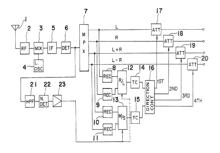
Referring to Fig. 1, a block diagram of the FM
stereo receiver according to the first embodiment of the
present invention is shown. In Fig. 1, reference number 1
is the antenna through which is received the FM stereo
broadcast signal; 2 is the RF amplifier which amplifies the
RF signal received by the antenna 1; 3 is the mixing
circuit which mixes the amplified RF signal and the output
signal of the local oscillator 4 to generate the IF signal;
5 is the IF amplifier which amplifies the IF signal; 6 is
the FM signal detector which detects the amplified IF
signal; and 7 is 'the stereo multiplexer which separates the
left and right stereo signals (L) and (R) from the stereo
sum signal (L+R) and stereo difference signal (L-R)
contained in the output signal from FM signal detector 6.
The stereo sum signal (L+R) is also referred to as a main
signal (M) and the stereo difference signal (L-R) is also
refexred to as a sub-signal (S).
Still referring to Fig. 1, reference numbers 8
through 11 are first through fourth rectifiers which
rectify the respective output signals of the stereo
multiplexer 7; 12 is a first comparison circuit which
calculates a ratio (R/L) of the levels of the signals
produced from the first and second rectifiers 8 and 9; 13
is a second comparison circuit which calculates a ratio
(M/S) of the levels of the signals produced from the third
and fourth rectifiers 10 and 11; 14 and 15 are first and
r~ ~ ~J ~)
~. .~ CJ C)
- 6 -
second time constant circuits connected to the output
terminals of the first and second comparison circuits 12,
13, respectively; 16 is a directional controller which
generates first through fourth output signals based on the
output signals of the first and second time constant
circuits 14 and 15; and 17 through 20 are first through
fourth attenuators which attenuate the output signals of
the stereo multiplexer 7 based on the first through fourth
output signals of the directional controller 16.
Furthermore, reference number 21 is a high pass
filter which passes high frequency noise in the detected
output signal; and 22.is a noise detector which detects the
high frequency noise and generates a control signal which
is outputted through a buffer amplifier 23 to control the
dynamic range of the second comparison circuit 13.
It is to be noted that the directional controller
16 and first through fourth attenuators 17 - 20 define a
level control circuit.
In operation, the FM stereo signal received at
the antenna 1 is RF amplified, converted to an IF signal,
and FM detected as in known FM stereo receiver. By the
stereo multiplexer 7, the left and right stereo signals (L)
and (R) are separated from the stereo sum signal (L+R) and
the stereo difference signal (L-R) contained in the output
signal of the FM signal detector 6. It is thus possible to
produce left and right stereo signals (L) and (R), stereo
f
~~.~ ~ ~ ~;~t~
- 7 -
sum signal (L-~-R), and stereo difference signal (L-R) at the
output terminals of the stereo multiplexer 7. The signals
obtained at the output terminal of 'the stereo multiplexer 7
are rectified by the first through fourth rectifiers 8 -
11, and are applied to the first comparison circuit 12 and
the second comparison circuit 13, respectively. An output
signal corresponding to the level ratio of the left and
right stereo signals (L) and (R) is generated by the first
comparison circuit 12, and an output signal corresponding
'to the level ratio of the stereo sum and difference signals
(L+R), (L-R) is generated by 'the second comparison circuit
13. A detailed description of the first and second
comparisran circuits 12 and 13 is provided for example in
U.S. Patent application Serial No. 381,922 which is
assigned to the same assignee as the present application,
or in European Patent publication EP 351,835 published
January 24, 1990.
The first and second output control signals from
the first and second comparison circuits 12 and 13 are
applied through the first and second time constant circuits
14 and 15, respectively, and in turn applied to the
directional controller 16.
Depending on the output signals from comparison
circuits 12 and 13, directional controller 16 carries out a
predetermined logic to generate first through fourth output .
signals. The first through fourth output signals from
~~ .~ il ~)
g
directional controller 16 are used far cantrolling the
first through fourth attenuatars 17, 18, 19 and 20.
For example, if the first and second output
control signals from the first and second comparison
circuits 12 and 13 indicate that the left stereo signal (L)
is dominant, the directional contraller 16 produces a low
level signal for the first output signal, and at the same
time, high level signals for the second, third and fourth
output signals. accordingly, attenuator 17 inserted in a
line for sending the left stereo signal (L) is not
activated, but other attenuators 18, 19 and 20 inserted in
lines for sending the right sterea signal (R), stereo sum
signal (L+R), and stereo difference signal (L-R) are
activated so that these signals (R), (L+R) and (L-R) will .
be attenuated a specific amount, thereby emphasizing the
left stereo signal (L). Note that the output signals of
the first and second comparison circuits 12, 13 vary
linearly as shaven in Figs. 3a and 3b according to the level
ratio of the left and right stereo signals (L) and (R) or
the level ratio of the stereo sum signal (L+R) and the
stereo difference signal (L-R). When the level ratio
becomes positive or negative, it is detected in the
directional controller 16 that the sound from a certain
direction should be emphasized. 11 detail of the
directional controller 16 is disclosed, for example, in
_ g _
'S.S. Patent No. 4,799,260 issued January 17, 1989 or in GB
A1 2,174,275 published October 29, 1986.
When there is very little or no noise signal in
the received signal, the noise detector 22 which compares
the noise signal in the received signal with a
predetermined level, produces a LOW level signal which is
in turn generated by buffer amplifier 23. The LOW level
output signal from buffer amplifier 23 is applied to second
comparison circuit 13. In this case, the secand comparison
circuit 13 operates normally.
However, when the noise signal in the received
signal increases due, for example, to multipath noise, the
noise level contained in the output signal of the FM signal
detector 6 also increases. This noise signal is detected
by the noise detector 22, and the output signal from the
buffer amplifier 23 has a level corresponding to the
detected noise level. When the output signal of the buffer
amplifier 23 is app7.ied to the second comparison circuit
13, the dynamic range of the second comparison circuit 13
is reduced.
In other words, as the noise signal in the
detected signal produced from detector 6 increases, the
noise signal in the output signal, of the stereo multiplexer
7 increases. Accordingly, the output signal from
multiplexer 7 is rectified and applied to the second
comparison circuit 13. If the noise detection circuit 21,
~'~~'.9~t~t~~
~ .9 ,:7
- 10 -
22 and 23 of the present invention is not provided, 'the
second comparison circuit 13 carries out the dominant
signal detection based on 'the noise signal. Accordingly,
the noise signal will be emphasized. Thus, without the
noise detection circuit 21, 22 and 23, the correct
directional emphasis can not be carried out.
According to the present invention, since the
noise detection circuit 21, 22 and 23 is provided, even if
the noise signal increases, the dynamic range of the second
comparison circuit 13 is varied using the output signal of
the buffer amplifier 23. Thus, the noise signal can be set
aside from the dynamic range, and thus it is possible to
prevent adverse effects from the noise signal during
directional emphasis.
According to the embodiment shown in Fig. 1,
since the stereo difference signal (L-R) occupies a
relatively high frequency region in the FM stereo signal
spectrum resulting in such that the stereo difference
signal (L-R) is easily affected by the noise signal
resulting from multipath interference, only the second
comparison circuit 13 is coupled with the noise detection
circuit 21., 22 and 23. Thus, the result of the noise
detection is used.only for varying the dynamic range of the
second comparison circuit 13. However, it is possible to
further connect the output of the buffer amplifier 23 with
the first comparison circuit 12, as indicated by a dotted
6 > ~~ ~ ~ ~3
~~.~~ ~ ~4;,~
- 11 -
line. In such a case, the output signal of the buffer
amplifier 23 may also be used to simultaneously vary the
dynamic range of the first comparison circuit 12.
Referring to Fig. 2, a sample circuit composing
the second comparison circuit 13 is shown, in which the
output signal of the third rectifier 10 is applied to the
first input terminal 13a, the output signal of the fourth
rectifier 11 is applied to the second input terminal 13b,
and an output signal corresponding to the level ratio of
the stereo sum arid difference signals (L+R)/(L-R) is
generated at the output terminal 13d connected to the
output side of the comparator 13c. Furthermore, collectors
of third and fourth transistors 13g and 13h composing the
current mirror circuit are connected to the collectors of
the differentially cannected first and second transistors
13e and 13f. Accordingly, the collector current of the
third and fourth transistors 13g and 13h is determined
according to, the current flowing to the current source 13i.
When the current flowing to the current source 13i varies
and is set to a specified level, it is possible to assure a
dynamic range with sufficient breadth, and also to prevent
the generation of unwanted output signals when there is no
input.
More specifically, when there is little noise in
the output signal of the FM signal detector 6, the output
of the buffer amplifier 23 is LOW and thus no control
l) r)
~t~.~ h~~.~a~7
7.2 -
signal is applied to the control -terminal 13j. In this
case, -the current flowing to the current source 13i is
maintained at a relatively low specified level. Tr7hen the
noise in the output signal of the FM signal detector 6
increases, the output signal level of -the buffer amplifier
23 applied to the control -terminal 13j increases.
Accordingly, the current flowing to the current source 13i
increases. Thus, the collector current of the third and
fourth transistors 13g and 13h increases, resulting in the
decrease of the dynamic range of the circuit shown in Fig.
2. Thus, the operational errors caused by the noise signal
can be prevented.
Referring to Fig. 4, a block diagram of the FM
stereo receiver according to a second embodiment of the
present invention is shown. When compared with the first
embodiment shown in Fig. 1, the second embodiment further
has first and second separation circuits 24 and 25 and a
provisional level control circuit 26. The first separation
circuit 24 separates the output signal of the first time
constant circuit 14 into the dominant left signal 24a and
the dominant right signal 24b which are applied to
directional controller 16. Similarly, the second
separation circuit 25 separates the output signal of the
second time constant circuit 15 into 'the dominant sum
signal 25a and the dominant difference signal 25b. The sum
signal 25a .is applied to the directional controller 16, but
a ,~)s ~ ~~ ~ f'3 ;~J
'~J .~. a L. ~5 ~3
- 13 -
the difference signal 25b is applied to the directional
controller 16 through the provisional level control circuit
26. In the second embodiment, the output of the buffer
amplifier 23 is connected to the provisional level control
circuit 26 which controls the level of the output dominant
difference signal of the second separation circuit 25
according to the output signal of the noise detection
circuit 21, 22 and 23.
In operation, the first and second output control
signals from the first and second comparison circuits 12
and 13 are applied through the first and second time
constant circuits 14 and 15, respectively, to the first and
second separation circuits 24 and 25. The first separation
circuit 24 separates the first control signal into the
dominant left signal 24a and the dominant right signal 24b,
and the second separation circuit 25 separates the second
control signal into the dominant sum signal 25a and the
dominant difference s9.gna1 25b. Figs. 6a, 6b, 6c and 6d
show the separated results, i.e., the dominant left signal,
dominant right signal, dominant sum signal, and dominant
difference signal, respectively. The output signals of the
first and second separation circuits 24 and 25 are applied
to the directional controller 16, so that one of the output
signals from the stereo multiplexes '7 is emphasized in a
similar manner described above.
~~f~~'~l~E~~~
For example, if only the dominant left signal is
generated in the output signals of the first and second
separation circuits 2~ and 25, the right stereo signal (R),
stereo sum signal (L+R), and stereo difference signal (L-R)
will be attenuated by a specific level according to the
second, third and fourth output signals from the
directional controller 16, thus emphasizing the left stereo
signal (L).
When there is little naise in the received
signal, a LOW level output signal is generated from the
buffer amplifier 23. In this case, the provisional level
control circuit 26, to which this LOW level output signal
is applied, is so set as to present an amplifier with a
gain equal to one. Thus, the output dominant difference
signal 25b from the second separation circuit 25 is applied
to the directional controller 16 with no substantial
change.
However, when noise in the received signal
increases to increase the output level from the noise
detection circuit 21, 22 and 23, the provisional level
control circuit 26 is so set as to present an amplifier
with a gain less than one. Thus, the output dominant
difference signal 25b from the second separation circuit 25
is applied to the directional controller 16 with reduced
level relative to the detected naise level.
ty
;~ ~. ~~ ~~ ;~ r~
- 15 -
In other words, when the noise signal caused
particularly by the multipath interference increases, the
output dominant difference signal of the second separation
circuit 25 increases relative to such noise signal due to .
the fact that the stereo difference signal (L-R) occupies a
.relatively high freguency region in the FM stereo signal
spectrum. Thus, without the provisional level control
circuit 26, it is not possible to obtain correct
directional emphasis.
According to the second embodiment shown in Fig .
4, since the provisional level control circuit 26 is
inserted in a Line for the dominant difference signal 25b,
it is possible to prevent supply of a erroneous dominant
difference signal caused by such noise to the directional
controller 16.
The provisional level control circuit 26 may be
arranged in such a manner that its output characteristics
varies linearly when the output signal from the noise
detection circuit 21, 22 and 23 is LOW level. When the
output signal from the noise detection circuit 21, 22 and
23 increases, the provisional level control circuit 26
reduces its gain to a predetermined gain less than one,
such as indicated by a single-dot/dash line shown in Fig.
6d, or alternati~rely, reduces its gain relatively to the
increase of the noise level, as indicated by a double-
dot/dash line in Fig. 6d. When the output 25b is varied in
t~~.V~ ~ ~r3
- 16 -
a manner shown in Fig. 6d, it becomes more difficult to
reach the threshold TH1 (Fig. 3b) as the noise level
becomes greater. Thus the adverse effects of noise can be
avoided. Two examples of the provisional level control -
circuit 26 are shown in Figs. 5b and 5c,
In Fig. 5b, the provisional level control 26
includes a transistor. When the signal produced from
buffer amplifier 23 and applied to the base of the
transistor varies linearly from low to high relatively to
the increase of the detected noise signal, the conductivity
of the transistor changes linearly. In this case, the
transistor serves as a variable resistor which. changes the
resistance in accordance with -the detected noise signal
level > On the other hand, when the signal applied to the
base of the transistor varies in a step between high and
low levels, the transistor serves as a switch for turning
on and off in accordance with the presence and absence of
the noise signal.
In Fig. 5c, the provisional level control 26 is
defined by a voltage control amplifier. When the signal
from the buffer amplifer 23 is applied to V~~, the gain of
the voltage control amplifier changes relatively to the
level of the signal produced. from buffer amplifier 23.
Thus, the dominant difference signal 25b as produced from
the separation circuit 25 is provisionally attenuated by
the gain change of the voltage control amplifier.
_ 17
It is to be noted that noise generated in the
presence of mul-ta_path interference significantly affects
the stereo difference signal (L-R), but it also effects -the
left and right stereo signals (L) and (R) and the stereo
sum signal (L+R). Thus, the provisional level control
circuit may also be inserted to the output signal paths of
each of the outputs from the first and second separation
circuits 24 and 25, as shown in Fig. 5.
Referring to Fig. 7, a block diagram of the FM
stereo receiver according to a third embodiment of the
present invention is shown. When compa-red with the first
embodiment shown in Fig. 1, the third embodiment further
has first and second holding circuits 27 and 28 which are
inserted between first comparison circuit 12 and first time
constant circuit 14 and between second comparison circuit
13 and second time constant circuit 15, respectively.
Also, the output of the buffer amplifier 23 in this
embodiment is connected to each of holding circuits 27 and
28. The first holding circuit 27 holds the output signal
of the first comparison circuit 12 according to the output
signal of the noise detection circuit 21, 22 and 23, and
similarly, the second holding circuit 28 holds the owtput
signal of the second comparison circuit 13 according to the
output signal of the noise detection circuit 21, 22 and 23.
In operation, when 'there is little or no noise
signal in the received signal, the noise detection circuit
~~~ ~ ~~t~:~~~~
_ 18 --
21, 22 and 23 produces a ~OT~1 level signal which is applied
to 'the first and second holding circuits 27 and 28. In
'this case, the first and second holding circuits 27 and 28
is so operated as to merely pass the signal therethrough
without any substantial change. Thus, the output signals
of the first and second comparison circuits 12 and 13 are
applied directly to the first and second time constant
circuits 14 and 15.
However, when noise in the received signal
increases, the signal from the noise detection circuit 21,
22 and 23 increases to a HIGH level signal correspondingly
to the detected noise. During the increasing of the output
signal from the noise detection circuit 21, 22 and 23, the
first and second holding circuits 27 and 28 are activated
to hold the signal. level of the output signals from the
first and second comparison circuits 12 and 13 immediately
before the noise signal becomes great. The values held in
the first and second holding circuits 27 and 28 are applied
to the directional controller 16.
Thus, it is possible to prevent the output signal
of the first and second comparison circuits 12 and 13 from
being applied to the directional controller 16 when the
signals from comparison circuits 12 and 13 cantain noise
signals. Thus, erroneous directional emphasis can be
prevented.
- 19 -
Instead of providing two hold9_ng circuits 27 and
28, as shown in Fig. 7, it is also possible to provide only
one, particularly the second holding circuit 28, at the
output terminal of the second comparison circuit 13 so that
the signal corresponding to the stereo difference signal
(L-R), which is the signal easily affected by noise as
described above, is controlled relative to the noise level
obtained from the noise detection circuit 2:1, 22 and 23.
Referring to Fig. 8, an example of the second
holding circuit 28 is shown. The second holding circuit 28
comprises a switch 36 which opens and closes according to
the output signal of the buffer amplifier 23, and a
capacitor 37 which when the switch is open holds the value
immediately before the switch opened. Therefore, when
noise is not present, the output of the buffer amplifier 23
is LOW, the switch 36 is maintained close. Thus, the
output signal of the second comparison circuit 13 is
applied to the second time constant circuit 15 through the
switch 36 and at the same time the signal level is stored
in capacitor 37. When noise is present, the output of the
buffer amplifier 23 becomes HIGH, resulting in opening of
switch 36. Thus, the input terminal of the second time
constant circuit 15 thereafter receives a signal level
corresponding to the output signal level of the second
comparison circuit 13 immediately before the switch 36
opened. Thus, the signal applied to the directional
~~J ~r
- 20 -
controller 16 from 'the second time constant circuit 15 will
not be affected by noise signal.
Referring to Fig. 9, another example of the
second holding circuit 28 is shown wherein the second time
constant circuit 15 is improved to function as the second
holding circuit 28. The second time constant circuit 15
comprises a first switch 38, a first time constant circuit
41 composed of a first resistance 39 and a first capacitor
40, a second time constant circuit 44 composed of a second
resistance 42 and a second capacitor 43, a third time
constant circuit 47 composed of a third resistance 45 and a
third capacitor 46, a window comparison circuit 48, and a
second switch 49 which is switched according to the output
of the buffer amplifier 23.
It is to be noted that the first switch 38 is
normally in the state as shown in Fig. 9, and switches from
this to the other position when a LOW signal is output from
the window comparison circuit 48. In addition, the second
switch 49 is opened by a HIGH output signal from the buffer
amplifier 23.
When there is no noise present, 'the output of the
buffer amplifier 23 is LOW, and the second switch 49
closes. In this state, if the output signal of the second
comparison circuit 13 is within the specified range of the
reference voltage, the output of the window comparison
circuit 4& becomes HIGH, and the first switch 38 is held in
,~ ~ '~ r 't~ ~~
- 27. -
the state as shown i.n Fig. 9. Thus, the output of the
second comparison Circuit 13 is connected to 'the output
terminal 50 through the first time constant circuit 41
having a high time constant and the second time constant
circuit 44 having a low time constant.
When the output signal of the second Comparison
circuit 13 becomes greater than a first predetermined
reference voltage B1, or lower than a second predetermined
voltage B2, the output of the window comparison circuit 48
becomes LOW, and the first switch 38 switches to the
position opposite 'that shown in Fig. 9. Thus, the output
signal of the second comparison circuit 13 is connected to
the output terminal 50 through only the second time
constant circuit 44.
When noise occurs, the output of the buffer
amplifier 23 becomes HIGH, and the second switch 49 opens.
Thus, because the first switch 38 switches to the position
shown in Fig. 9, and the output of the second comparison
circuit 13 is connected to the output terminal 50 through
the first time constant circuit 41 with the high time
constant, the output signal of the second comparison
circuit 13 is held in Capacitor 40. Therefore, according
to the circuit shown in Fig. 9, the time constant circuit
15 can be arranged to functional as the holding Circuit 28.
It is to be noted that the second switch 49 which opens and
closes according to the output signal of 'the buffer
/1 d r~ I~ !)
.ri.
- 22
amplifier 23 may also be connected to ane side of the third
capacitor 46 of the third time constant circuit 47, as
shown by a dotted line.
Referring to Fig. 10, a block diagram of the FM
stereo receiver according to a fourth embodiment of the
present invention is shown. When compared with the first
embodiment shown in Fig. 1, the fourth: embodiment further
has a controllable low pass filter 54 connected to the
output of attenuator 20. Also, the output of noise
detection circuit 21, 22 and 23 is connected to the
controllable low pass filter 54 which cuts off the high
frequency signal in accordance with the signal obtained
from the noise detection circuit 21, 22 and 23.
In operation, when there is little or no noise
signal in the received signal, the noise detection circuit
21, 22 and 23 produces a hOW level signal which is applied .
to the controllable low pass filter 54. In this case, the
controllable low pass filter 54 is so operated as to merely
pass the signal therethrough without any substantial
change. Thus, the output signal o~ the attenuator 20 is
outputted without any change.
However, when noise in the received signal
increases, the signal from the noise detection circuit 21,
22 and 23 increases to a H7CGH level signal corresponding to
'the detected noise. When the output from 'the noise
detection circuit 21, 22 and 23 increases, the controllable
_ 23 _
low pass filter 54 is gradually activated to cut off the
high frequency signal components wr~ich are mostly occupied
by the high frequency noise signals. Thus, as the output
level from the noise detection circuit 21, 22 and 23
increases, the degree of cutting the high frequency .
component becomes greater.
Tnstead of the noise detection circuit 21, 22 and
23, it is 'possible to employ an electric field strength
detection circuit for detecting the electric field strength
of the received signal, such a level detector for detecting
the FM IF signal level.
Referring to Fig. 11, an example of the
controllable low pass filter 54 is shown, which, comprises a
first and second amplifier 55 and 56 for amplifying the
output signal from attenuator 20, a low pass filter 57 for
cutting off the high frequency signal from the output
signal of the second amplifier 56, and an adder 58 for
adding the output from the first amplifier 55 and the low
pass filter 57. The gain of each of the first and second
amplifiers 55 and 56 are controlled linearly with respect
to the output level of the buffer amplifier 23.
In operation, when there is little or no noise
signal in the received signal, the noise detection circuit
21, 22 and 23 produces a LOW level signal. Thus, the gain
of the first amplifiers 55 and 56 are set, respectively, to
the maximum and minimum levels. Thus, the output signal
.3, -o r !~ ~ r3
9 1J
2 y ~.
from attenuator 20 is transmitted -through the first
amplifier 55 and adder 58 and to output -terminal 59. In
this case, no filtering is effected in low pass filter 57
and, therefore, the output signal from attenuator 20 is
outputted from the output terminal 59 with no substantial
change.
When noise signal in the received signal
increases, the signal from buffer amplifier 23 increases
corresponding to the detected noise. Thus, the gain of the
first amplifier 55 gradually decreases, and at the same
time, the gain of the second amplifier 56 gradually
increases. The output from the second amplifier 56 is
applied to the low pass filter 57 in which the high
frequency component is cut off. Thus, at the adder 58, the
stereo difference signal of entire frequency range and the
stereo difference signal with high frequency signal
component being removed are added and the combined signal
is outputted from terminal 59.
When noise signal in the received signal becomes
very high, the signal from buffer amplifier 23 becomes
maximum. Accordingly, the gain of the first amplifiers 55
and 56 are set, respectively, to the minimum and maximum
levels. Thus, the output signal from attenuator 20 is
transmitted through the second amplifier 56, low pass
filter 57 and adder 58 and to output terminal 59. In this
case, output terminal 59 produces the stereo difference
- 25 -
signal with 'the high frequency z~ignal component being cut
off with the maximum rate.
Tt is to be noted 'that in any of the embodiments
described above, the stereo sum signal (L+R) and the stereo
difference signal (L-R) output from the stereo multiplexer
7 are considered to be included in the output signal of the
FM signal detector 6, but the stereo sum signal (L+R) and
the stereo difference signal (L-R) may also be generated by
adding and subtracting the separated left and right stereo
signals (L) and (R).
Furthermore, in any of the embodiments described
above, a level control circuit is used in which four output
signals are produced from the stereo multiplexer 7, and
each signal is separately applied to an attenuation circuit
for the level control, but other arrangement for the level
control can be used: For example, it is possible to employ
such an arrangement that the level control processing is
first applied to the left and right stereo signals (L) and
(R), and these level-cowtrolled left and right stereo
signals (L) and (R) are used to produce the stereo sum and
difference signals (L-HRj and (L-~R) .
As will be known to those skilled in the art from
the preceding description of an FM stereo receiver
according to the present invention, because directional
emphasis based on the condition of the received signal is
y possible, an apparent improvement in separation can be
(9 ~ i~ ~ rl
-. 2 6 -
achieved, and it is therefore possible to increase audio
presence. Specifically, because noise included in the
received signal is detected, erroneous directional emphasis
caused by noise can be prevented, and correct directional
emphasis can be applied.
According to the present invention, the detected
noise signal is used to control the pro-log~.c surround
system such that the dynamic range of at least the second
comparison circuit is changed when the noise increases, or
that the output signal level of at least the second
comparison circuit is held when the noise increases, or
that the level of at least the dominant difference signal
is controlled using the second level control circuit when
the noise increases.
Although the present invention has been fully
described in connection with the preferred embodiments
thereof with reference to the accompanying drawings, it is
to be noted that various changes and modifications are
apparent to those skilled in the art. Such changes and
modifications are to be understood as included within the
scope of the present invention as defined by the appended
claims unless they depart therefrom.