Note: Descriptions are shown in the official language in which they were submitted.
2017561
The present invention relates to an image forming
apparatus wherein an electrophotographic photosensitive
member is scanned by a light beam modulated in accordance
with signals indicative of the image to be recorded to form
a latent image thereon, and the latent image is developed.
One of such image forming apparatuses is a laser beam
printer of an electrophotographic type which is advantageous
in the high speed recording and low noise. In this printer,
so-called binary level recording wherein the laser beam is
lit on or off in accordance with the image signal. In order
to record a halftone image in the laser beam printer of the
binary level recording, a dither method, density pattern
method or the like are known. As is known, however, the
dither method and the density pattern method are not suitable
to provide a high resolution image. Recently, a proposal has
been made as to the system for recording a halftone image
without reducing the record density and the resolution. In
this system, the halftone image is recorded by modulating a
width of a pulse signal for driving the laser in accordance
201~561
with the image signal. More particularly, the on-period of
the beam per one picture element of the laser is controlled
in accordance with the density of the image to be recorded.
In other words, the exposure period of the photosenstivie
member per one picture element (pixel) by the laser beam
scanning the photosensitive member is controlled in
accordance with the density of the image. More particularly,
the pulse width is short for the low density portion of the
image to provide the long exposure period, whereas the pulse
width is long for the high density image portion to provide
the longer exposure period. In accordance with the pulse
width modulation system (PWM system), the image can be formed
with high resolution and high tone gradation, and is
particularly suitable for a color image forming apparatus
which requires the high resolution and the high tone
gradation.
BRIEF DESCRIPTION OF THE DRAWINGS
Figure 1 is a sectional view of an image forming
apparatus according to an embodiment of the present
invention.
Figure 2 is a perspective view of an optical system
used in the apparatus of Figure 1.
Figures 3 and 4 show a pulse width modulating circuit
used in the apparatus of Figure 1 and signal waveforms
therefrom, respectively.
Figures 5A and 5B show exposure distributions on a
photosensitive member in a conventional apparatus.
Figures 6A, 6B and 6C show exposure distributions on
the photosensitive member.
~ .~
2D17561
Figures 7A and 7B illustrate tone production by area
change of the dot.
Figure 8 is a graph showing a V/D characteristics of
a known developing system.
Figure 9 is a graph showing the relation between the
pulse width modulation and the image density in accordance
with the present invention.
Figure 10 is a graph showing toner particle size
distribution of the toner used in the apparatus according to
the embodiment of the present invention.
Figure 11 is a graph showing the relation between the
average particle size of the toner and the m;n;mllm
reproducible dot diameter.
Figure 12 is a sectional view of a developing
apparatus according to an embodiment of the present
invention.
Figure 13 is a somewhat schematic view of an image
forming apparatus according to another embodiment of the
present invention.
Figure 14 is a sectinal view of a developing
apparatus according to a further embodiment of the present
nvent lon .
Figures 15A and 15B show on/off of the laser source
an output distribution for each pixel of the CCD.
Figure 16 shows distribution of the laser spot
diameter.
- 4 - 2017~61
In the aforementioned PWM system, the area tone
gradation is possible for the dot formed by the beam spot per
one pixel, and therefore, the halftone gradation is
represented without decreasing the density of the pixels
(recording density).
However, it has been found that the exposure
distribution on the scanned surface (surface of the
photosensitive member) is influenced by the spot diameter of
the laser beam, as shown in Figures 5A and 5B. In these
Figures, the exposure distributions on the scanned surface
are shown under the following conditions:
Density of pixels: 400 dpi (unit pixel size is 63.5
microns)
Laser spot diameter: 70 microns (the diameter at
1/e2 in the main scan Gauss distribution)
Laser on-period: the duration corresponding to 1/4
pixel (25 ~)/unit pixel, and the duration corresponding to
1/2 pixel (50~)/unit pixel.
Usually, the diameter of the laser beam spot on the
surface to be scanned is considered as being optimum when it
is 1.1 - 1.6 times the size of the unit pixel to provide most
uniform exposure distribution when all of the pixels are
exposed in consideration of the interference by the adjacent
pixels. When the record density is 400 dpi, the laser beam
spot diameter is approximately 70 - 100 microns (1/e2
diameter). Therefore, the ratio of the laser beam spot size
to the unit pixel size is 1.1 - 1.6. In Figures 5A and 5B,
the laser beam spot diameter is within this range.
When the halftone image is to be recorded using the
laser beam spot diameter described above, the exposure
distribution on the photosensitive member does not change
very much as shown in Figure 5B, even if the laser beam is
2017~61
-- 5
turned on and off to provide the pulse width which is 50 ~ of
the pulse width providing the m~l mllm density, per unit
pixel, and the contrast between the maximum exposure amount
and the minimum exposure amount (the contrast will be
described in detail hereinafter), is not sufficient
(approximately 30 ~), with the result that the tone gradation
in the record by the area change of the dot in each of the
pixels provided by the developing process is not stabilized.
When the laser beam spot diameter described above is
used, the exposure distribution on the scanned surface has a
small amplitude as shown in Figures 5A and 5B when the laser
is turned on and off, the contrast is low with the tendency
of the average exposure amount of the scanned surface
entirely shifts. When the halftone image is recorded through
the PWM system, the surface potential on the photosensitive
drum tends more to be shifted as a whole in response to the
laser driving pulse width change because of the above-
described exposure distributions. Therefore, the produced
output image is strongly influenced by the V-D
characteristics (r characteristics) which will be described
in detail in conjunction with Figure 9, of the developing
system, with the result that the output image density does
not change linearly in response to the laser driving pulse
width (PWM signal) change (this will be described in
conjunction with Figure 8A). In order to solve this problem,
an image processor is conventionally provided with a
correction reference table for correcting the PWM signal to
provide the linear change of the output image density in
consideration of the V-D characteristics of the developing
system. However, when the amount of correction by the
correcting table is large, there arise problems such as void
of the image information, improper tone gradation. In
addition, the amount of correction is increased when the V-D
characteristics are changed due to the change in the ambient
/
:
- 6 - 2017S61
conditions such as ambient temperature and humidity or the
like.
SUMMARY OF THE INVENTION
Accordingly, it is a principal object of the present
invention to provide an image forming apparatus in which a
light beam on-period per one pixel is controlled in
accordance with signals indicative of the image to be
recorded, thus recording an image, wherein the image can be
formed with high resolution and with high tone reproduction.
It is another object of the present invention to
provide a color image forming apparatus capable of forming a
color image with high resolution and high tone reproduction.
These and other objects, features and advantages of
the present invention will become more apparent upon a
consideration of the following description of the preferred
embodiments of the present invention taken in conjunction
with the accompanying drawings.
DESCRIPTION OF THE PREFERRED EMBODIMENTS
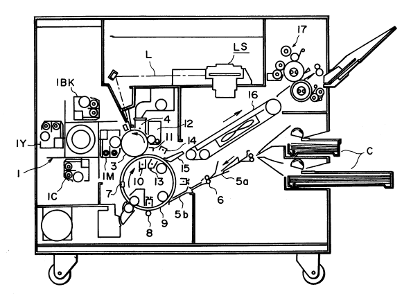
Referring to Figure 1, there is shown a color printer
of an electrophotographic type to which the present invention
is applicable.
The printer includes an electrophotographic
photosensitive drum 3 (image bearing member) rotatable in a
direction of an arrow. Around the photosensitive drum 3,
there are disposed a charger 4, a rotary type developing
apparatus 1 having developing devices lM, lC, lY and lBK, an
image transfer discharger 10, cleaning means 12 and a laser
beam scanner LS disposed at the upper position in the
drawing. These elements constitute an image forming means.
A
7 _ 20175Cl
Each of the ...............................................
~ ,~
8-
developing devices is effective to supply to the drum 3
a two-component developer comprising toner particles
and carrier particles. The developing device 1M
contains magenta toner; the developing device 1C
contains cyan toner; the developing device 1Y contains
yellow toner; and the developing device lBK contains
black toner.
The original to be copied is read by an
unshown original reader. The reader has photoelectric
transducer elements such as CCD (charge coupled device)
or the like for converting an image of an original to
electric signals. It produces image signals
corresponding to magenta image information, cyan image
information, yellow image information and black-white
image information of the original, respectively. A
semiconductor laser contained in the printer is
controlled in accordance with the image signal to
produce a laser beam L. It is possible to print out
output signal from a computer.
The sequence of the operation of the color
printer will be briefly described, taking as an example
the full-color mode. First, the photosensitive drum 3
is uniformly charged by the charger 4. The
photosensitive drum 3 is then scanned with and exposed
to the laser beam L modulated in accordance with
magenta image signal, so that an electrostatic latent
image is formed on the photosensitive drum 3. The
9 2U~
latent image is reverse-developed by a magenta
developing device 1M already brought to the developing
pos ition .
The transfer material such as paper is
supplied from a cassette C along the sheet guide 5a, a
sheet feeding roller 6 and a sheet guide 5b. The
transfer material is held by a gripper 7 of a transfer
drum 9 and is electrostatically retained thereon by the
function of a contact roller 8 and an opposite
electrode therefore. The transfer drum 9 rotates in
the direction indicated by an arrow in synchronism with
the photosensitive drum 3. The magenta developed image
provided by the magenta developing device 1M is
transferred onto the transfer material by the transfer
charger 10 at the transfer station. The transfer drum
9 continues to rotate as it is, and it is prepared for
receiving the next color image (cyan in the example of
Figure 1).
On the other hand, the photosensitive drum 3,
after being subjected to-the image transfer operation,
is electrically discharged by the charger 11 and then
is cleaned by the cleaning means 12. It is then
charged again by the charger 4 and is exposed to the
laser beam L now modulated in accordance with thé cyan
component image signal, so that an electrostatic latent
image is formed on the photosensitive drum 3. During
this, the developing apparatus 1 rotates to present the
-10- ~ ~
cyan developing device 1C to the predetermined
developing position to reverse-develop the cyan latent
image to form a cyan toner visualized image.
The above process is repeated for the yellow
image signal and the black image signal. When the
image transfer operations for the four color visualized
(toner) image are completed, the transfer material is
electrically discharged by chargers 13 and 14, and the
gripper 7 is released to permit the transfer material
to be separated from the transfer drum 9 by the
separation pawl. The separated transfer material is
conveyed on the conveyer belt 16 to an image fixing
device 17 of heat-pressure-roller type, where the four
visualized images overlaid on the transfer material are
fixed at once. In this manner, the series of the full-
color printing sequential operation is completed, and a
full-color print is formed.
As shown in Figure 12, the exposure means
includes a semiconductor laser 102, a polygonal mirror
105 rotating at a high speed and an f-0 lens 106. The
semiconductor laser 102 produces a laser beam L which
is modulated in accordance with time-series digital
picture element (pixel) signals produced by the image
reader or by an electronic computer or the like. The
laser beam L thus produced is projected on the surface
of the photosensitive drum. The laser beam L is
projected to such a portion of the drum 3 where the
7~
toner is to be deposited, and therefore, the developing
device reverse-develops the latent image by which the
toner particles charged to the same polarity as the
charging polarity by the charger 4 is deposited on the
right potential portion of the latent image.
With continued reference to Figure 2, the
semiconductor laser element 102 which is the laser
source is connected with a laser driver 500 which
functions as an emitting signal generator for supplying
an emitting signal (driving signal) for producing the
laser beam. The laser is lit on and off in accordance
with the emitting signal of the laser driver. The
laser beam L emitted from the laser element 102 is
substantially collimated by a collimator lens system
103. The collimator lens system 103 is movable in the
direction of an arrow A coaxial with the optical axis
of the laser beam by focus adjusting means 104 which
includes a rack on which the lens system 103 is fixed,
a pinion meshed with the rack and a motor for driving
the pinion.
The polygonal mirror, that is, the rotatable
mirror 105 having plural reflecting surfaces rotates at
a constant speed in the direction of an arrow B to
scanningly deflect the collimated beam through the
collimator lens system 103. The fO lens system 106
(106a, 106b and 106c) disposed in front of the
polygonal mirror 105 functions to form a spot on the
-12- ~7~
surface to be scanned, that is, the surface of the
photosensitive drum 3 from the laser beam deflected by
the polygonal mirror 105, and to provide a constant
scAnning speed on the surface to be scanned. The
direction of movement of the beam L on the drum 3 by
the polygonal mirror 105, that is, the direction
indicated by the arrow c is called "main scan
direction". The main scan direction is a direction
with a movement direction of the surface of the drum 3
in the exposure station, preferably substantially
perpendicular thereto. On the other hand, the movement
detection of the drum 3 in the exposure station is
called "sub-scan direction". By the main scan and the
sub-scan, the surface of the photosensitive drum 3 is
raste-scanned by the laser beam.
Before the start of the modulation in
accordance with the signal indicative of the image to
be recorded, the laser beam L is directed to a CCD
(charge coupled device) 108 functioning as a detecting
means, through a reflection mirror 107. The CCD 108
has a number of photoelectric transducer element
arranged in the direction C at a position optically
equivalent to the surface of the photosensitive drum 3.
The CCD 108 is connected with a controller 100 for
controlling the laser driver 500 and the focus
adjusting means 104.
The signal processor 111 is connected with the
-
-13-
laser driver 500 and the controller 100.
With the above structure, when a desired image
is to be formed, an image output signal P is supplied
from the signal processor 111 to the controller 100,
and an image signal S is supplied to the laser driver
500 to turn on and off the laser element 102 in
accordance with the image signal S.
By the scanning with the laser beam L, an
exposure distribution corresponding to one main scan is
formed on the photosensitive drum 3 surface. With each
of the main scans, the photosensitive drum 3 is rotated
through a predetermined amount, so that a latent image
is formed on the photosensitive drum with the exposure
distribution corresponding to the image signal S. The
image output signal P is supplied to the signal
processor 111 prior to the image signal S. After the
completion of the supply of the image signal S, the
output thereof is terminated. The controller 100
disables the focus adjusting means 104 during the
period in which the image processor 111 supplies the
image output signal P.
The operation of the focus position adjusting
means 104 for the laser beam L will be described.
While the image output signal P is not
produced, an actuation signal is supplied from the
controller 100 to the laser driver 500. From the laser
driver 500, a rectangular wave turned on and off at
~17~S~
-14-
regular intervals as shown in Figure 15A is generated
for a predetermined period of time, and in accordance
with the test signal, the laser element 102 is turned
on and off. The laser beam modulated in accordance
with the test signal is reflected by the reflection
mirror 107 and is projected and scan the CCD 108
disposed at a position optically equivalent with the
photosensitive drum 3.
The controller 100 clear the accumulated
charge of the photoelectric transducer elements of the
CCD 108 before the laser beam L scans the CCD 108.
After electric charge is accumulated on the
photoelectric transducer elements of the CCD 108 by one
line scanning with the laser beam modulated in
accordance with the test signal, the charge is read as
an electric signal.
The exposure amount distribution on the CCD
108 is as shown in Figure 16 in which the distribution
pattern is in accordance with the spot diameter of the
laser beam L. Therefore~ the distribution of the
outputs of the photoelectric transducer elements of the
CCD 108 is as shown in Figure 15B, and the signal
representing it is supplied to the controller 100. The
controller 100 calculates a contrast V which is defined
by:
V = (Omax-Omin)/(Omax+amin) ...(1)
where Omax is the maximum of the output of the CCD, and
-15-
Omin is the minimum of the output. The value V
is associated with a laser beam spot diameter measured
in the scanning direction on the photosensitive drum.
More particularly, in this case, the contrast V defined
above increases with decrease of the spot diameter in
the scanning direction.
Therefore, the comparison is made between a
predetermined contrast Vo (which corresponds to a
target spot diameter of the laser beam in the scanning
direction on the photosensitive drum) and the contrast
V calculated by the equation (1). If the contrast V is
not equal to the predetermined contrast level Vo, the
controller 100 produces a driving signal to the focus
ad;usting means 104 to shift the collimator lens system
103 in the direction A through a distance corresponding
to the difference between the contrasts V and Vo. At
the position of the collimator lens 103 after the
movement, the contrast V is again measured, and the
collimator lens 103 is finally fixed at a position
where the contrasts V and Vo are equal. By doing so,
the focus deviation of the optical system attributable
to the thermal expansion of the supporting means or the
like can be corrected to minimize the diameter of the
scanning spot of the laser beam L.
It is preferable that the spot diameter
control operation for the laser beam is performed
immediately before each start of the electrostatic
-16- ~ ~
latent image formations for the color components. By
the laser beam spot diameter control, a desired spot
diameter can be obtained, and therefore, good image
forming operation can be performed.
Referring to Figure 3, the PWM circuit will be
described. In Figure 3, the PWM circuit includes a TTL
latching circuit 401 for latching 8 bit image signal, a
level converter 402 for converting the TTL logic level
into a high speed ECL logic level, an ECLD-A converter
403, an ECL converter 404 for producing the PWM signal,
a level converter 405 for converting the ECL logic
level to the TTL logic level. A clock generator 406
for producing clock signals 2f having the frequency
which is twice of the pixel clock signal f, a
triangular wave generator 407 for generating
substantially ideally triangular wave signal in
synchronism with the clock signal 2f, and 1/2 frequency
divider 408 for dividing the frequency of the clock
signal 2f by 2. For the purpose of high speed
operation in the circuit, the ECL logic circuit is
disposed at various parts.
Referring also to Figure 4, the description
will be made as to the operation of the circuit, Figure
4 showing the waveform of the signal.
A signal (a~ is a clock signal 2f, and signal
(b) is a pixel clock signal f having a double
frequency, and is associated with the pixel number, as
-17-
shown in the Figure. In order to maintain the duty
ratio of 50 % of the triangular signal also in the
triangular wave generator 407, the clock signal 2f is
temporarily divided by 2, and then, the triangular
signal (c) is generated. Further, the triangular
signal (c) is converted to the ECL level (0 - -1 V),
and is now the triangular wave signal (d).
On the other hand, the pixel signal varies
over the range of 256 tone gradation levels from OOH
(white) - FFH (black). The mark H represents hexa-
expression. The image signal (e) shows the ECL voltage
level after the D/A conversion. In Figure 4, the first
pixel has the FFH voltage level which is for the
maximum density; the second pixel has the 80H voltage
level which is intermediate; the third pixel has the
40H voltage level which is for an intermediate density
level lower than the second pixel; and the fourth
picture element has the 20H voltage level which is for
an intermediate density lower than the third pixel.
A comparator 404 compares the triangular
signal (d) and the image signal (e), and produces PWM
signals having pulse widths corresponding to the pixel
density to be formed. In the example of Figure 1,
these pulse widths are indicated by T, t2, t3 and t4,
where T > t2 > t3 > t4. The PWM signals are converted
to the TTL levels which are either 0 V or 5 V into the
PWM signals (f) which is a laser driving pulse signals
2~17~
-18-
(256 kinds of signals including zero). The PWM signals
(f) are supplied to the laser driving circuit 500.
Thus, the semiconductor laser 102 emits, for each of
the pixels, a laser beam for a period corresponding to
each of the pulse widths of the signals (f) to
sc~nn; ngly expose the photosensitive member 3 thereto.
In the printer of this embodiment, the reverse
development is effected, and therefore, the laser beam
emitting period is longer if the image density is
higher.
In the circuit of Figure 3, the upstream side
of the latching circuit 401 is equipped with an unshown
look-up table. The look-up table is for a r correction
(tone gradation correction) of the image data and is
the memory storing the r-corrected data. The memory is
accessed by the address data which is the 8-bit image
signal per picture element, so that the r-corrected
image signal is outputted. Usually, a particular one
~-correction table is used in one frame or page, but it
is possible that several kinds of r-correction tables
are prepared, and some of them are used selectively in
the frame. That is, three tables are sequentially and
repeatedly used for the respective line scans by the
beam, so that the r-correction in the sub-scan
direction is changed line by line to correct the tone
gradation.
The look-up table or tables are prepared so
201756~
that the correction thereof is not influenced by the
densities inherent to the respective color toners,
i.e., the yellow toner, the magenta toner, the cyan
toner and the black toner. More particularly, when the
density of the toner is low, the correction table is
prepared on the basis of a steep r curve, whereas when
the density is high, the opposite property r table is
prepared. Thus, the r tables are provided for the
respective colors. Upstream of the look-up table, it
is possible that a non-linear color masking circuit,
for example, a secondary color masking circuit, may be
provided to correct turbidity.
-In the color printer shown in Figure 1, the
PWM circuit (Figure 3) is sequentially supplied with
the yellow, the magenta, the cyan and the black image
signals for each of the pages (one page of the original
and copy). The image signals are sequentially
modulated for the respective colors. By four rotations
of the drum 3, one color copy is produced. In the
apparatus of Figure 13 which will be described
hereinafter, the PWM circuit is provided for each of
the colors.
In this embodiment, at the upstream of the
look-up table provided for each of the colors, a non-
linear masking circuit is provided to correct theturbidity for each of the colors. The masking circuit
is in the form of a secondary color masking circuit,
-20- 201756~
for example. This is effective, together with the use
of the small size laser spot and the small size toner
particles which will be described hereinafter, to
provide finer and high grade color images with good
tone gradation and color reproduction.
When a small size spot is imaged from the
pulse width modulated laser beam on the photosensitive
drum through the optical system shown in Figure 2 to
form a tone gradation, the exposure distribution on the
photosensitive drum surface is as shown in Figure 5B,
where the beam spot diameter measured along the main
scan direction on the drum surface is 1.1 - 1.6 times
the size of the unit pixel record measured in the main
scan direction, even if the laser beam is rendered on
and off for a unit pixel with the pulse width of 50 %
of the maximum pulse width corresponding to the maximum
density. The contrast which has been defined
hereinbefore between the maximum and minimum levels of
the exposure amount is as small as approximately 3Q %,
with the result that the subsequent development process
does not provide the stabilized tone gradation
utilizing the area change in each of the dots.
Various experiments and investigations made by
the inventors have revealed that in order to stabilize
the tone reproduction by area change per dot using the
pulse width modulation of the laser beam, the contrast
defined hereinbefore in the exposure distribution on
-21- 2~56~
the image bearing member is not less than approximately
80 % when the laser beam is rendered on and off with
the pulse width of 50 % of the above-described maximum
pulse width, for example.
Referring to Figure 6, the comparison will be
made between when the ratio of the beam spot size
measured in the detection of the main scan on the image
bearing member to the size of the recording pixel
measured in the direction of the main scan (spot size
ratio) is not more than 0.7 and when it is larger than
0.7 as in the prior art.
It is added here that the strength
distribution of the laser spot is a Gaussian
distribution. Therefore, when the beam spot diameter
or size referred to in this Specification is the so-
called 1/e2 diameter, that is a diameter of a
circumferential line connecting the points, in the
distribution, which have the strength of the 1/e2
multiplied by the maximum strength.
Figures 6A, 6B and 6C show the exposure
distribution on the drum surface under the conditionthat the recording density is 400 dpi (unit pixel size
is 63.5 microns), in a case (A) wherein the laser beam
spot size is 1.1 times (70 microns) the picture element
size (Figure 6A), in a case (B) wherein it is 0.8 times
(50 microns) (Figure 6C), and in a case (C) wherein it
is 0.7 times (42 microns) (Figure 6C). The contrasts
20~75~;~
-22-
provided in these cases are shown in Table 1 below.
Table 1
(A) (B) (C)
Spot size ratio 1.1 0.8 0.7
Pulse width 50% ON 50% ON 50% ON
Contrast 30% 60% 85%
As will be understood from the above Table 1,
the contrasts of the exposure distribution are
approximately 30 % ~case (A)), approximately 60 % (case
(B)) and approximately 80 % (case (C)) when the laser
beam is rendered on and off with the pulse width of 50
% of the maximum driving pulse width, for each of the
picture elements. Thus, it is understood that the
contrast not less than 80 % can be provided by
selecting the laser beam spot size measured in the main
scan direction (1/e2 size) to be not more than 0.7
times the picture element size measured in the main
scan direction.
Figures 7A and 7B show the configuration range
of the dot provided by forming a latent image and
developing it by the subsequent developing process,
when the laser driving pulse width is changed from 10 %
2017~
-23-
- 100 % of the maximum driving pulse width, for each of
the spot diameters. The spot size measured in the sub-
scan direction was 1.1 times the picture element size
measured in the sub-scan direction (70 microns) as in
the prior art to make the exposure distribution uniform
in the sub-scan direction.
Figure 8 is a graph showing the results
illustrated in Figures 7A and 7B. In Figure 8, the
abscissa represents a width of the laser driving pulse
(a ratio relative to the maximum pulse width for one
picture element); and the ordinate represents the
density (reflection density) of the resultant image
developed.
Figure 9 shows the V-D characteristics (tone
gradation characteristics) of the development system.
In Figure 9, the abscissa represents a surface
potential of the photosensitive member; and the
ordinate represents a density (reflection density) of
the resultant developed image.
Generally speaking, a developing system has a
threshold characteristics wherein the developing action
suddenly occurs at a predetermined level of the surface
potential of the photosensitive member, as shown in
Figure 9. Therefore, when the contrast of the exposure
distribution is low as shown in Figure 7A, the surface
potential of the photosensitive drum changes has a
whole, and therefore, as shown in Figure 8A, the
` - 2~175~;~
-24-
developer is deposited on the surface of the
photosensitive drum abruptly where the surface
potential exceeds the threshold level. As a result, as
shown in Figure 7A, the size of the developed dot
abruptly increases at a certain number of gradation
level.
On the contrary, where the laser beam spot
size measured in the main scan direction is 0.7 times
the unit pixel size to provide not less than 80 %
contrast of the exposure distribution in one pixel, the
pattern of the latent image formed on the
photosensitive drum has the high potential contrast in
accordance with the exposure distribution. Therefore,
even if the latent image is developed by a developing
system having a certain threshold level characteristic,
the exposure distribution has a higher level
immediately from a short driving pulse region to such
an extent that the development threshold level is
exceeded, and therefore, it is stably developed as a
dot (Figure 7B). As a result, the pixel can be
reproduced with the stably changed dot size from the
region having the smaller on/off ratio of the driving
pulse, by which the area changing gradation is stably
effected.
Figure 8B shows the image density vs. the
laser driving pulse when the spot diameter ratio
described above is used. As will be apparent from this
~01~
-25-
Figure, the image formation is not much influenced bythe developing system, and the stable area changing
gradation is possible in one pixel. Therefore, even if
the ambient temperature, humidity or the like changes
with the result of the change in the threshold level of
the developing system, the influence by such a change
is minimized since the image recording according to the
present invention is not easily influenced by the V-D
characteristics in the neighborhood of the threshold
level. Thus, the tone reproduction is further
stabilized.
In addition, even if the correcting reference
table for the correction of the PWM signals is such
that the output image density changes more linearly in
the image signal processing circuit, the missing of the
image information and the skipping of the tone
reproduction resulting from the correction can be
suppressed, since the amount of correction can be made
very small. Thus, the present invention is effective
to minimize the occurrence thereof, and in addition,
the correction error due to the change in the
developing properties attributable to the ambient
condition change can be suppressed.
As described hereinbelow, the laser beam spot
size measured in the main scan direction on the
photosensitive member is not more than 0.7 times the
unit pixel size measured in the main scan direction.
20~
-26-
Theoretically, the lower limit of the size is 0,
however, practically, it is difficult to reduce the
size to lower than 20 microns. However, the size of
the laser spot measured in the sub-scan direction is
preferably not less than 1.1 and not more than 1.6
times the unit pixel size measured in the sub-scan
direction in order to make the exposure distribution
uniform in the sub-scan direction. Therefore, in the
present invention, the configuration of the laser beam
spot formed on the photosensitive member is oval having
a minor axis substantially in the main scan direction
and a major axis substantially in the sub-scan
direction.
As regards the unit pixel, in order to provide
the equivalent recording density in the main scan
direction and the sub-scan direction, it is desirable
that the size of the pixel in the main scan direction
is the same as in the sub-scan direction.
In order to provide the laser beam spot size
and configuration on the photosensitive member as
described above, the use is made with a semiconductor
laser emitting a laser beam having a proper angle of
divergence and lenses 103 and 106 having proper power.
The selection or selections may be made without
difficulty within the scope of the present invention.
Even if the good tone reproduction can be
provided by the present invention, the image quality at
` -
-27-
the high light portion may be roughened as the case may
be due to the toner scattering during the image
transfer and/or image fixing operation.
As a result of various experiments and
investigations, it has been found that this problem can
be solved by adjusting the particle size distribution
of the toner and/or the volume average particle size of
the toner.
More particularly, according to this
invention, the toner particles contain not less than 90
% by volume toner particles satisfying (1/2)M < r <
(3/2)M where r is a particle size of the toner, and M
is a volume average particle size of the toner, and the
toner particles also contain not less than 99 % by
volume of the toner particles satisfying 0 < r < 2M.
Further, according to the present invention,
the volume average particle size of the toner is not
more than 12 microns, further preferably, not more than
9 microns, even further preferably not more than 8
microns and not less than 4 microns.
When the toner has a volume distribution
outside the range, the effects are not sufficiently
provided even if the average particle size is changed.
When the percentage of the toner particles in
the large particle size region in the volume
distribution, the number of toner particles having
large sizes which are contributable to the toner
zo~
-28-
scattering during the image transfer operation does not
decrease even if the average particle size is reduced.
Therefore, it is difficult to decrease the roughness in
the low image density area in the produced image by
reducing the average particle size. On the other hand,
if the number of toner particles in the small diameter
region in the volume distribution is increased, the
number of toner particles deposited on and not attached
from the carrier particles is relatively increased, and
therefore, the carrier particles are not able to
triboelectrically charge the toner particles with high
efficiency, so that the toner scattering from the
developing device is increased and that the production
of the foggy background is increased. The toner having
small particle size is relatively easily fused on the
surface of the carrier particles with the result of the
deterioration of the carrier particles and of the toner
scattering increased.
For the reasons stated above, the desired
volume distribution is as in Figure 10 wherein the
distribution is sharp.
Figure t1 is a graph showing a relation
between the volume average particle size of the toner
and the size of the dot of the minimum reproduction in
the image after the image fixing operation when the
laser beam spot is oval having a diameter of 70 microns
in the sub-scan direction and a diameter of 42 microns
` ~61 . -
-29-
in the main scan direction, and when the latent image
is formed on the photosensitive drum and is developed
into a toner image which is in turn transferred and
fixed.
The developing conditions were changed for
each of the toner particle sizes, by, for example,
using a DC biased AC developing bias or a DC bias, by
changing the material of magnetic carrier particles, by
changing the sleeve-drum clearance or by changing the
sleeve-blade clearance. However, they hardly
influenced the diameter of the minimum reproduced that.
This may be described in the following r nner.
In the system wherein a latent image is
written by the control of the on-period of the laser
beam, the density tone gradation of the development is
improved with the reduction of the size of the laser
spot size. However, when the images are transferred
and fixed a plurality of times in order to obtain a
full-color image, the large size toner particles
scatter with the result of a larger dot. On the
contrary, the small size toner particles are not easily
scattered, so that the image is not much disturbed.
This is because the small size toner particles
constitute a thin layer on the transfer sheet after the
image transfer, and therefore, the attraction force
with the sheet is large. Therefore, even when the
toner image is subjected to the image transfer electric
-30- ~
field a plurality of times, they are not easily
scattered.
The reproducibility in the full-color image at
the low image density area, is remarkably conspicuous
in the image. The impression of the image is
significantly different depending on whether or not the
dots having the size of approximately 50 microns are
faithfully reproduced or not, when the tone full-color
image is to be formed. Therefore, according to this
embodiment, the laser beam spot size in the main scan
direction is not more than 42 microns under the
condition that the recording density is 400 dpi; the
toner has a volume average particle size of not more
than 9 microns, further preferably not more than 8
microns. By doing so, the dot having the size of
approximately 50 microns can be faithfully reproduced,
and the scattering during the image transfer operation
is extremely reduced. In addition, the tone
reproducibility in the low density portions in the
full-color image is sufficient as contrasted to the
conventional method, and the fine image can be provided
with low roughness or blurness.
With the above advantageous effects,
particularly when the volume average particle size of
the toner is not more than 8 microns, the dot having
the size not more than 50 microns is faithfully
reproduced, and in addition, the image is not disturbed
-31- ~
even if it is subjected to the image transfer electric
field a plurality of times. Particularly, this
tendency contributes to the reproducibility and the
reduction of the image roughness in the low density
portion.
When the toner has the volume average particle
size of 6 microns, it is preferable that the volume
distribution of the toner is such that they contain not
less than 90 % by volume of toner particles having a
size exceeding 3 microns and not exceeding 9 microns,
and that they contain not less than 99 % by volume of
the toner particles having a size larger than 0 and
smaller than 12 microns.
The volume distribution and the volume average
particle size of the toner are measured in the
following manner:
A Coalter Counter TA-II (Coalter Corporation)
is used. To the counter, an interface ~Nikkaki
Kabushiki Kaisha, Japan) outputting a number average
distribution and a volume average distribution, and
CX-i personal computer (Canon gabushiki Kaisha, Japan)
are connected. Using electrolyte (first class natrium
chloride), 1 % NaCl water solution is prepared.
To the electrolyte solution (100 - 150 ml),
0.1 - 5 ml of surface active agent (dispersing agent)
(preferably alkylbenzene sulfonate) is added. Further,
0.5 - 50 mg of the material to be tested is added
-32-
20~
thereto.
The electrolyte suspending the material is
subjected to the ultrasonic dispersing treatment for
approximately 1 - 3 min. Using an aperture of 100
microns, the particle size distribution in the range of
2 - 40 microns is measured using the counter TA-II to
obtain the volume distribution.
From the volume distribution obtained, the
volume average particle size of the material is
obtained.
In order to produce the toner particles having
the sharp particle size distribution, as described
hereinbefore, the following method is preferable. The
material for the toner is melted and kneaded. It is
then cooled and pulverized, and the pulverized
particles are finely classified. Thereafter, the toner
is provided having the desired particle size
distribution and/or the volume average particle size.
In order to effect the precise classification,
the pulverized powder product may preferably be
classified by a fixed-wall type wind-force classifier
to obtain a classified powder product, and ultra-fine
powder and coarse powder are simultaneously and
precisely removed from the classified powder by means
of a multi-division classifier utilizing a Coanda
effect (e.g., Elbow Jet Classifier available from
Nittetsu Kogyo K.K.), thereby to obtain a toner having
-33- ~
a prescribed particle size distribution and/or volume-
average particle size.
In the present invention, the term "toner" may
include colored resin particles (comprising a binder
resin and a colorant and another optional additive) per
se, and colored resin particles to which an external
additive such as hydrophobic colloidal silica has been
externally added.
The binder resin used for the toner may for
example include: styrene-type copolymers such as
styrene-acrylic acid ester resins and styrene-
methacrylic acid ester resins; and polyester resins.
In view of color mixing characteristics at the
time of fixing, particularly preferred resins may be
polyester resins obtained through polycondensation of
at least a diol component selected from bisphenol
derivatives represented by the formula:
CH3
H-~OR ~ O ~ I ~ O-~RO~y H
CH3
wherein R denotes an ethylene or propylene group; x and
y are respectively a positive integer of 1 or more
providing the sum (x+y) of 2 to 10 on an average, and
their substitution derivatives, and a two- or more-
functioned carboxylic acid component or its anhydride
or its lower alkyl ester, such as fumaric acid, maleic
acid, maleic anhydride, phthalic acid, terephthalic
_34_ 2017~
acid and the like. Such polyester resins may show a
sharp melting characteristic.
Examples of the colorants suitable for the
purpose of the present invention may include the
following pigments or dyes. Not recommendables are
C.I. Disperse Y164, C.I. solvent Y77 and C.I. Solvent
Y93, which exhibit low light stability.
Examples of the dyes may include: C.I. Direct
Red 1, C.I. Direct Red 4, C.I. Acid Red 1, C.I. Basic
Red 1, C.I. Mordant Red 30, C.I. Direct Blue 1, C.I.
Direct Blue 2, C.I. Acid Blue 9, C.I. Acid Blue 15,
C.I. Basic Blue 3, C.I. Basic Blue 5, and C.I. Mordant
Blue 7.
Examples of the pigments may include: Naphthol
Yellow S, Hansa Yellow G, Permanent Yellow NCG,
Permanent Orange GTR, Pyrazolone Orange, Benzidine
Orange G, Permanent Red 4R, Watching Red calcium salt,
Brilliant Carmine 3B, Fast Violet B, Methyl Violet
Lake, Phthalocyanine Blue, Fast Sky Blue, and
Indanthrene Blue BC.
Particularly preferred pigments may include
disazo yellow pigments, insoluble azo pigments and
copper phthalocyanine pigments, and particularly
preferred dyes may include basic dyes and oil soluble
dyes.
Particularly preferred examples may include:
C.I. Pigment Yellow 17, C.I. Pigment Yellow 15, C.I.
-35-
201756~
Pigment Yellow 13, C.I. Pigment Yellow 14, C.I. Pigment
Yellow 12, C.I. Pigment Red 5, C.I. Pigment Red 3, C.I.
Pigment Red 2, C.I. Pigment Red 6, C.I. Pigment Red 7,
C.I. Pigment Blue 15, C.I. Pigment Blue 16, copper
phthalocyanine pigments having two or three carboxy-
benzamidomethyl groups, and copper phthalocyanine
pigments.
Particularly preferred examples of dyes may
include: C.I. Solvent Red 49, C.I. Solvent Red 52, C.I.
Solvent Red 109, C.I. Basic Red 12, C.I. Basic Red 1 and
C.I. Basic Red 3B.
As for the content of the colorant, a yellow
colorant for providing a yellow toner, which
sensitively affects the transparency of an OHP film,
may preferably be used in a proportion of 0.1 to 12 wt.
parts, more preferably 0.5 - 7 wt. parts, per 100 wt.
parts of the binder resin. A proportion of more than
12 wt. parts provides a poor reproducibility of mixed
colored of yellow, such as green, red and skin color.
A magenta colorant and a cyan colorant for
providing the magenta and cyan toners, respectively,
may preferably be used in a proportion of 15 wt. parts,
more preferably 0.1 - 9 wt. parts, per 100 wt. parts of
the binder resin.
In case of a black toner contained two or more
colorants in combination, the addition of more than 20
wt. parts in total is liable to cause spending thereof
-36-
2~
to the carrier and cause the colorants to be exposed on
the toner surface, thus inviting increased sticking of
the toner onto the photosensitive drum to instabilize
the fixability. For this reason, the amount of the
colorants in the black toner should preferably be 3 to
15 wt. parts per 100 wt. parts of the binder resin.
A preferred combination of colorants for
providing a black toner may be that of a disazo type
yellow pigment, a monoazo-type red pigment and a copper
phthalocyanine-type blue pigment. The proportional
ratios of the yellow pigment, the red pigment and the
blue pigment may preferably be 1:1.5 to 2.5:0.5 to 1.5.
It is also preferred to add a charge control
agent in order to stabilize the negative chargeability
to the toner according to the present invention. In
this instance, it is preferred to use a colorless or
thin-colored negative charge control agent so as not to
affect the color toner of the toner. The magnetic
charge control agent may for example be an organo-metal
complex such as a metal complex of alkyl-substituted
salicylic acid (e.g., chromium complex or zinc complex
of di-tertiary-butylsalicylic acid). The negative
charge control agent may be added to a toner in a
proportion of 0.1 to 10 wt. parts, preferably 0.5 to 8
wt. parts, per 100 wt. parts of the binder resin.
When the developer used in the present
invention is a two-component developer comprising a
-37-
carrier and a toner, the carrier may preferably
comprise magnetic particles. The magnetic particles
may preferably be those comprising ferrite particles
~maximum magnetization: 60 emu/g) which have been
coated with a resin so that they have a particle size
of 30 - 100 microns, more preferably 40 - 80 microns,
an electric resistivity of 107 ohm.cm or more, more
preferably 108 ohm.cm or more.
The resistivity of the magnetic particles is
measured with a sandwiching-type cell having a
measuring electrode area of 4 cm2 and having a
clearance of 0.4 cm between the electrodes. One of the
electrodes is imparted with 1 kg weight, and a voltage
E (vlcm) is applied across the electrodes, and the
resistivity of the magnetic particles is determined
from the current through the circuit.
Figure 12 is a sectional view of one of the
developing devices of the rotary type developing
apparatus 1 used with the laser beam printer shown in
Figure 1. Each of the d~veloping devices has the
similar structure. The developing device in Figure 12
is disposed at the developing position faced to the
photosensitive drum 3.
The developing device has a developing sleeve
opposed close to the photosensitive drum at the
developing zone where the developer is supplied to the
photosensitive drum. The developing sleeve 22 is made
-38- ~
of non-magnetic material such as aluminum, stainless
steel (SUS 316). The developing sleeve 22 is disposed
in an elongated opening of a developer container 36 at
the bottom left part of its wall. Substantially a half
circumference thereof is within the container 36. The
container 36 contains a two component developer
containing non-magnetic toner particles and magnetic
carrier particles. The other half circumference
thereof is exposed outside of the container. It is
rotatable in the direction indicated by an arrow b.
The developing sleeve 22 carries the two component
developer supplied thereonto in the container 36 to the
developing zone, where the developer is supplied to the
photosensitive drum 3. A magnetic brush of the
developer is formed on the sleeve 22 in the developing
zone and is lightly contacted to the drum 3.
In the developing sleeve 22, a stationary
permanent magnet 23 is disposed. The magnet 23 has a
magnetic pole 23a (N pole), a magnetic pole 23b (S
pole), a magnetic pole 23c (N pole) and a magnetic pole
23d (S pole), i.e., four magnetic poles. The magnet 23
may be in the form of an electromagnet rather than the
permanent magnet.
At the top edge of the opening of the
developer container in which the developing sleeve 22
is disposed, a non-magnetic blade 24 is disposed which
is fixed at a wall of the container at its base
~39~ ;~175~;3l
portion, and the other end thereof is disposed to the
sleeve 22. The sleeve extends along the length of the
opening and functions to regulate the thickness of the
layer of the developer to be conveyed to the developing
5 zone. The blade 24 is a stainless steel plate (SUS
316) having an "L" cross-section. Adjacent the non-
magnetic blade 24, there is disposed a magnetic
particle confining member 26 is provided which has a
developer guiding surface 261. The non-magnetic blade
10 24, the magnetic particle combining member 26 and the
like constitute the regulating portion.
The developer contains the magnetic carrier
particles 27 and the non-magnetic toner particles 37.
In order to seal the toner particles stagnating at the
15 bottom portion of the developer container 36, a sealing
member 40 is provided. The sealing member 40 has an
elasticity and therefore is vent along with the
rotational direction of the sleeve 22 to elastically
press to the surface of the sleeve 22. The sealing
20 member 40 has an end portion at the downstream portion
of the contact area with the sleeve with respect to the
rotational direction of the sleeve so as to permit the
developer to entire the container.
In the container, there is provided a
25 scattering preventing electrode plate 30 is provided to
apply a voltage to the suspending toner produced by the
developing action a voltage having the same polarity as
-
_40_ 2017S6~
the toner particles, thus depositing them to the
photosensitive drum 3 to prevent the scattering of the
toner. Also, in the container, there is disposed a
toner supplying roller 60 operated in accordance with
an output of a toner content detecting sensor (not
shown). As for this sensor, it may be of a developer
volume detecting type, piezoelectric element type,
inductance change detecting type, an antenna type using
an alternating bias voltage, an optical density
detecting type or the like. The non-magnetic toner
particles 37 are supplied by the rotation of the roller
60. The fresh developer with the supplied toner 37 is
conveyed by a screw 61, while they are mixed and
stirred. Therefore, the triboelectric charge is
applied to the supplied toner during the conveyance. A
partition plate 63 is partly cut away ad;acent
longitudinal opposite ends of the developing device,
where the fresh developer conveyed by the screw 61 is
transferred to a screw 62. The S pole 23d is a
conveying magnetic pole to receive the developer after
being subjected to the developing operation and to
convey the developer to the regulating portion in the
container. Adjacent the S pole 23d, the screw 62
disposed close to the sleeve functions to exchange the
developer collected after the developing operation with
the fresh developer.
The conveying screw 64 is to uniformize the
_41- 2017561
quantity of the developer along the length of the
developing sleeve 22. The developer conveyed on the
developing sleeve by the rotation of the sleeve is
conveyed in the direction of the length of the sleeve
by the screw 64. By this, a part of the developer
layer having a projected portion on the sleeve is
pushed back, that is, is moved in the direction
opposite to the conveying direction of the developer on
the sleeve, through a space M of Figure 12. The screw
64 functions to convey the developer in the direction
opposite to the direction by the screw 62.
The structure of the developing device is
usable when the magnetic particles and weakly magnetic
or non-magnetic toner particles are mixed in the
developer container.
The edge of the non-magnetic blade 24 and the
developing sleeve 22 are spaced by a clearance d2 of 50
- 900 microns, preferably 150 - 800 microns. If the
clearance is smaller than 50 microns, the magnetic
particles are easily clogged in the clearance with the
result of non-uniform developer layer formation and-
with the result of insufficient developer applied on
the sleeve, which leads to a low density and non-
uniform image provided. In order to prevent in the
clogging of the clearance by the agglomerated toner
contained in the developer and other foreign particles,
the clearance d2 is preferably not less than 400
-
-42-
~1
microns. If it is larger than 900 microns, the amount
of the developer applied on the developing sleeve 22 is
increased, and therefore, the desired thickness of the
developer layer is not obtained. In this case, the
quantity of the magnetic particles deposited onto the
photosensitive drum is increased, and the developer
regulation by the circulation of the developer and the
action of the developer containing member 26 become not
enough with the result of insufficient triboelectric
charge of the toner which leads to production of the
foggy background.
The angle a1 in the Figure is -5 - 35 degrees,
preferably 0 - 25 degrees. If 01 < -5 degrees, the
developer thin layer provided by the magnetic force,
image force and/or agglomeration force applied to the
developer is sparse and non-uniform. If 01 > 35
degrees, the amount of the developer layer applied
increases when the non-magnetic blade is used, so that
it becomes difficult to provide the desired amount of
developer.
To the sleeve 22, a vibratory bias voltage
which is a DC biased AC voltage is supplied from the
source 31, by which between the drum 3 and the sleeve
22 in the developing zone, a vibratory electric field
is formed in which the direction of the field
alternately changes in short period. By the vibratory
electric field, the toner makes vibratory motions, by
-43-
2~1756~
which the toner becomes more easily releasable from the
surface of the carrier particles and the surface of the
sleeve, so that the electrostatic latent image can be
developed with a high development efficiency. Here,
the light portion potential and the dark portion
potential of the latent image is between the top and
bottom peaks of the vibratory bias voltage. When a DC
voltage is to be superposed, the voltage thereof is
preferably at a level between the light portion
potential and the dark portion potential.
In the printer in the embodiments, the reverse
development is effected, and therefore, the toner is
charged to the same polarity as the dark portion
potential of the latent image.
In the developing device, the used toner has
the particle size distribution and the particle size
satisfying the above-described conditions. For
example, the toner having the volume average particle
size of 6 microns is used. The clearance d2 between
the non-magnetic blade 24 and the developing sleeve 22
surface was 600 microns. The clearance between the
developing sleeve 22 surface and the photosensitive
drum 3 was 450 microns.
The photosensitive drum 3 was made of a
laminated type organic photoconductor (OCP). The light
portion potential of the latent image where the toner
particles were to be deposited was -150 V, and the dark
-44-
portion potential which constituted the background was
-600 V. The bias voltage source provided a rectangular
wave AC voltage having a frequency of 1700 Hz and the
peak-to-peak voltage of 1500 V biased with a DC voltage
of -300 V.
On the photosensitive drum, a magentar a cyan,
a yellow and a black images were formed in this order.
The semiconductor laser produced a laser beam having a
spot size on the drum of 42 microns in the main scan
direction and 70 microns in the sub-scan direction.
The on-period of the laser beam was controlled in
accordance with the driving pulse width control
described in the foregoing in accordance with the color
separated original image information. The image was
written at the density of 200 lines/inch and with 256
tone gradations to form latent images. They were
sequentially developed and transferred, and finally
fixed. By this, a full-color image was produced
wherein the light image density portion were faithfully
reproduced, and the image quality was high without the
roughness.
On the contrary, when the laser beam spot
diameter was 70 microns in the direction of the main
scan, and the toner particles having the volume average
particle size of 12 microns were used, and the image
was produced under the same conditions, the
reproducibility of the image in the light image density
-45-
2~1756~.
portion was poor, and the image was rough, as compared
with the image formed with the toner having the average
particle size of 6 microns.
Figure 13 shows another image forming
apparatus to which the present invention is applicable.
In this embodiment, the image forming
apparatus is in the form of a full-color laser beam
printer, but as contrasted to the foregoing embodiment,
the apparatus is provided with the image bearing
members for the respective colors. More particularly,
it comprises an electrophotographic photosensitive drum
3Y for yellow image formation, a drum 3M for magenta
image formation, a drum 3C for cyan image formation and
a drum 3BK for black image formation. Around the
respective drums, the laser beam scanners 80Y, 80M, 80C
and 80BK are disposed, respectively. Also, around the
respective drum, there are disposed a developing
devices 1Y, 1M, 1C and 1BK; image transfer dischargers
10Y, 10M, 10C and 1OBK; and cleaning devices 12Y, 12M,
12C and 12BK.
The transfer material is sequentially conveyed
along the sheet guide 5a, by the feeding roller 6 along
the sheet guide 5b to the attraction charger 81 by
which it is corona-charged to be assuredly attracted on
the conveying belt 9a.
Thereafter, the images formed on the
respective photosensitive drums are sequentially
-46-
;~0175~
transferred superposedly onto a transfer material by
the chargers 10Y, 10M, 10C and 1OBK, respectively. It
is discharged by a discharger 82 and is separated from
the conveying belt 9a, and the image is fixed by the
fixing device 17 into a full-color image. Also, when
the above-described transfer system is used, the laser
beam spot size in the scAnn~ng direction is not more
than 42 microns under the condition that the recording
density is 400 dpi, and the developing device shown in
Figure 12 is used. The toner has the volume average
particle size of less than 12 microns, preferably not
more than 9 microns, and further preferably not more
than 8 microns and not less than 4 microns is used. By
doing so, the good tone gradation and with less toner
scattering were obtained even at the low image density
portions, so that a fine full-color image can be
produced.
The detailed examples will be described,
concentrating on the toner.
Example 1
Polyester resin obtained by
condensation of propoxidized
bisphenol and fumaric acid
(weight-average molecular
weight (Mw) = 15,000, number-average
molecular weight m(Mn) = 3,300) 100 wt.parts
Rhodamine pigment 5 wt.parts
-
-47-
Negative charge control agent
(metal complex of di-alkyl-
substituted salicylic acid) 4 wt.parts
A mixture containing the above ingredients in
the prescribed amounts was melt-kneaded. After
cooling, the kneaded product was pulverized and the
pulverized product was classified by means of a fixed-
wall type wind-force classifier and further classified
by means of a multi-division classifier utilizing a
C~n~ effect to obtain negatively chargeable magenta
toner having a volume-average particle size of 6
microns.
The thus obtained magenta toner had a sharp
particle size distribution such that it contained 95 %
by volume of particles having a particle size of above
3 microns and below 9 microns, and substantially 100 %
by volume of particles having a particle size of above
0 microns and below 12 microns.
0.4 wt. part of negatively chargeable
hydrophobic colloidal siLica was mixed with 100 wt.
parts of the above-mentioned magenta toner to prepare a
magenta toner containing externally added silica (i.e.,
external addition product). Then, 6 wt. parts of the
magenta toner (external addition product) was mixed
with 94 wt. parts of ferrite magnetic particles coated
with a styrene-acrylic acid ester copolymer (weight-
average particle size: 50 microns, electric
-48-
201756~
resistivity: 101 ohm/cm) to prepare a two-component
developer for forming a magenta toner image.
By using cyan, yellow and black colorants
shown in the following Table 2, a two-component
developer for forming a cyan toner image, a two-
component developer for forming a yellow toner image;
and a two-component developer for forming a black toner
image were respectively prepared in the same ~nner as
described above.
--49--
.
a
,~ T ~
O O O
~- æ~
.0 .~,
n v
a) ~ ~ 'l
~ ~ O~ V
2~75~
-50-
Each of the two component developers is poured
into a polyethylene resin container having a volume of
100 ml, and it is shaked by hands approximately 30
times, and then, triboelectric charge of the toner is
measured. The measurements for the respective color
toner particles were approximately -30 micro-coulomb/g.
The two component developer was supplied to
the color image forming apparatus shown in Figure 1.
In the developing device of this embodiment, the
clearance d2 between the non-magnetic blade 24 end and
the developing sleeve 22 surface was 600 microns, and
the clearance d1 between the developing sleeve 22
surface and the photosensitive drum 3 surface was 450
microns.
The photosensitive drum 3 was a laminated type
organic photoconductor (OPC), and the light portion
potential was -150 V, while the dark portion potential
was -600 V in the latent image.
The bias voltage source provided a rectangular
wave AC voltage having a-frequency of 1700 Hz and a
pea~-to-peak voltage of 1500 V biased with -300 V DC
voltage.
On the other hand, the semiconductor laser
source provided a laser beam having a spot diameter
(1/e2 diameter) of 42 microns in the main scan
direction, and the 1/e2 diameter of 70 microns in the
sub-scan direction. The above-described driving pulse
-51-
widtn control was effected to control the emitting
period. The image was written at the density of 200
lines/inch and with 256 tone gradation. The reverse
development and the electrostatic image transfer were
repeated sequentially, and finally, the images was
fixed by a heating and fixing roller to produce a full-
color image. Then, the image was high quality and
sufficiently fine without roughness, wherein the light
image density portion (high light portion) was
faithfully reproduced.
When the resultant full-color image was
observed, the dots having the size of 50 microns were
faithfully reproduced, corresponding to the latent
images.
Examples 2 - 4
Similarly to the Example 1, the toners having
the volume average particle size of 5 microns, 6.8
microns and 8 microns were prepared, as shown in Table
3 below. The full-color images was produced in the
similar manner as in the-Example 1~ The results were
similarly good.
20~7561
--52--
a
o
o o o O
~1 U! O O O
oa ~ ~ ~ ~
-~ N
U~
O ~
V
'1 ~i
'
C ~
In ~D
u, ~ ~ a~
~ o a, ~
a~ oP u a)
'~ ~ N V
52 ~--1
~ S~ U~
E~ O
a
a)
N
-rl
Ul
0
_l a ~ ~ o~
~ -1 G
O ~
:~ ~0
~7
a~
Q-
X X X
` - 20175~
-53-
Comparison Example
Similarly to the Example 1, the respective
color toner particles having the volume average
particle size of 12 microns were prepared, as shown in
Table 4.
Table 4
Volume average Vol. ~ of toner Vol. % of toner
particle size particles having particles having
of toner a siæe > (1/2)M a size > O and
and ~ (3/2)M < 2M
Magenta toner 12 85 97
Cyan toner 12 85 97
Yellow toner 12 85 97
Black toner 12 85 97
--55-
Similarly to the Example 1, the two component
developer was prepared, and the color image was formed.
In the resultant image, as compared with the image by
the Example 1, the roughness of the image was
remarkable, although the reproducibility was good even
at the low image density portion.
The two component developer is poured into a
polyethylene resin container having a volume of 100 ml,
and it was shaked by hands approximately 30 times, and
the triboelectric charge of the toner was measured. It
was -16 - -18 micro-coulomb/g for each color toner, it
was lower as compared with the case of Example 1.
When the provided full-color image was
observed, the minimum dot size in which the latent
image was faithfully reproduced was approximately 90
microns. For the smaller dots, the scattering was
remarkable.
Example 5
Similarly to the Example 1, each color toner
having the volume average particle size of 9 microns
was prepared, as shown in Table 5. Similarly to the
Example 1, the two-component developer was prepared.
The color image was formed in the manner
similar to the Example 1. The resultant image was fine
and of high quality with less roughness and with
faithful reproduction of the low image density portions
(high light portion), although the image was slightly
- ~017~G1
-56-
poorer than the image by the Example 1.
When the full-color image was observed, the
dots having the size of approximately 60 microns were
faithfully reproduced, and the dots having the size of
approximately 50 microns were relatively faithfully
reproduced with respect to the latent image.
20175S~
--57--
L
a ,~
o ~ ~
o o o o o
U~ o o o o
o a) ~ ~ ~ ~ ~
d~ C~ a)
,1 N
Ll u~ tN
O ~
V
L ~_
r :~
o
/~
r) o a
dP C) ~
~1 ~ N V
~I Ll U~ ~5
E~ g ~
a)
~ N
Ll -~1
O L
a
~-~1 o
I
~I Ll
O ~
> P~ O
a L
a L
O L ~ ~,
a o
o
o
- O X
a) ~
m
- 20175~
-58-
In the foregoing embodiments, the two
component developer having ferrite carrier particles,
and a vibratory bias voltage is applied to the sleeve;
and the bias voltage is in the form of an AC bias
voltage which is DC-biased. However, the present
invention is applicable to the case wherein the two
component developer contains usual ion particles as the
carrier, and a DC bias voltage is applied to the
sleeve.
When the developing device having the
structure shown in Figure 14 was used, and when the
developing sleeve was rotated in the opposite
direction, that is, the peripheral surface of the
developing sleeve was moved in the opposite direction
from the photosensitive drum in the developing zone.
It was confirmed that the similar advantageous effects
were obtained when the average particle size was not
more than 8 microns.
The present invention is applicable not only
to the so-called contact-type developing device wherein
the developer is contacted to the photosensitive member
in the developing zone but also to the so-called non-
contact type developing apparatus wherein the
thickness of the developer layer carried on the sleeve
is smaller than the clearance between the
photosensitive member and the sleeve in the developing
zone.
-59-
The present invention is also applicable to
the developing device using a one component developer
not containing the carrier particles.
The use of the present invention is not
limited to the color printer described above, but is
applicable to a printer (monochromatic printer) using
the electrophotographic process wherein the tone
reproduction is important.
While the invention has been described with
reference to the structures disclosed herein, it is not
confined to the details set forth and this application
is intended to cover such modifications or changes as
may come within the purposes of the improvements or the
scope of the following claims.