Note: Descriptions are shown in the official language in which they were submitted.
72896-25
CORRELAT~D ~LIVER LATCH
Fielcl of t~e Invention
The invention relates to VLSI circuit design and, more
particularly, to the use of simple flow-through latches to perform
as functional replacements for master-slave flip flops in a VLSI
desiyn. Most high speed computers make use of bi-stable elements
or state devices, such as latches and flip flops. The type of
state devices used in the computer, in conjunction with the
synchronous clocking scheme employed for the state devices,
determines the speed and efficiency of high speed computers.
Backqround of the Invention
Synchronous clocking systems are set up such that data
flows from one group of state devices to the next, synchronized
with the clock. In computer systems, generally, the synchronous
clocking is either single phase or multi-phase. The type of clock
system chosen for a computer design is based upon the type of
state device chosen in the design along with other timing
constraints.
The two most common types of state devices used in
typical high speed computers include the so-called "flip flop and
latch" or "master-slave flip flop". A flip flop is an electronic
state device capable of exhibiting either of two stable states and
of switching between these states in a reproducible manner. In a
logic circuit, the two states are made to correspond to logic 1
and logic O. Flip flops are therefore one-bit memory elements
which are used in digital processors.
Flip flops are available in various forms including "D
flip flops" and "master-slave flip flops". A D flip flop is a
~.
' '
2 72896-25
clocked flip flop having a single input ~. The D flip flop outp~t
Q ta]kes on ~he current state of the D input only when a given
transition of the clock signal occurs between its two logic
states. A master-slave flip flop includes master and slave
elements that are clocked on complementary transitions of the
cloc]c signal. Data is only transferred from the master element to
the slave element, and hence to the output, after the master
device outputs have stahilized. Master-slave operation eliminates
the possibilities of ambiguous outputs, which can occur in single
element flip flops as a result of propagation delays in driving
the flip flops.
A latch is a state device that can be considered as an
extension of a flip flop, which temporarily stores a single bit of
data. The storage is controlled by a clock signal, a given
tran~ltion of which fixes the latch output at the current value of
lts input. During the period in which the clock signal is open,
data supplied to the input of the latch flo~s through to the latch
output (flow-through latch). Generally, master-slave flip flops
contain two latches i.e. a master and a slave. These state
devices can be described with respect to their various parameters
which are defined below and used throughout the specification:
"C" is the cycle time or period for the clock cycle.
"Tpd" is the propagation delay time through the state
device and is defined as the time interval between a change on the
device's clock or data input until the corresponding change on the
output.
''TSu'' is the "data to clock set up" time for a state
device and is defined as the minimum time interval during which
` - . ' ' ' - . . : :
. . . -: :
:' . .. . ~ . . - .
' . , , . :.
.. . . ..
3 72896-25
the device data input must be held stable before the arrival of
the latching edge of the clock pulse.
"Thld" is the clock to "data hold time" for a state
device and is defined as the minimum time interval during which
the device data input must be held stable after the latching edge
of the clock pulse has been removed.
"S" is the clock skew defined as the undesired
difference between arrival times of the clock signals at any pair
of destinations, where the arrival times are expected to be
substantially identical.
"W" is the width of the clock pulse, corresponding to
the time period in which a latch is held open.
"MIN" or "MINIPATH" is the minimum amount of delay
necessary to insure a race-free transfer of data between two state
devices.
"MAX" or "MAXPAT~" is the maximum amount of delay that
is allowed between two state devices.
Prior computers have extensively used master-slave flip
flops in their VLSI designs. To operate properly on a VLSI chip,
however, master-slave flip flops typically require twice as much
power and twice as much area as a simple latch.
The use of only one simple latch in place of a master-
slave flip flop or state device in a VLSI design has been very
difficult to implement due to the timing constraints imposed by
the necessary clocking required. There is therefore a need for a
simple latch design which functions as a master-slave flip flop
replacement while operating properly in conjunction with the
synchronous clock system of a high speed computer.
4 72896-25
Summary of the Invent on
The present invention makes use of latches which
function as mast~r-slave flip flops yet require approximately half
of the area and half of the power of a master-slave flip flop for
proper operation in a VLSI design. The latch system is
synchronously clocked by a pulse generator which produces sliver
or narrow pulses to reduce the minimum and maximum amount of delay
necessary to approximate the operation of the master-slave flip
flop. Further, the pulse generator makes use of the correlation
among state devices formed on a VLSI chip to eliminate the
problems of regulating the pulse width size. Sliver pulses from a
single pulse generator are used to clock the state devices
similarly located on the same chip. Overall, a single chip can
have multiple sliver pulse generators.
The present invention comprises a first flow-through
latch havlng an input, and output and a clock input.
A pulse generator circuit in the invention produces
narrow pulses coupled to the clock input of the first latch
wherein the first latch and the pulse generator are physically
spaced in close proximity to each other in a VLSI chip to take
advantage of the correlation factor among state devices on the
same chip.
It is therefore an advantage of the present invention to
provide a correlated sliver latch which functions as a master-
slave flip flop. The invention substantially reduces the power
requirements for the master-slave flip flop as well as the area
requ~rements needed on the VLSI chip.
It is a further advantage to allow the clock scheme to
. : ' :
.:
' ' : - . ~ .
,: ' ' ' . '' ': , ' ~ ' :
: .
7289G-25
be distributed at a 50% duty cycle. This i5 accomplished without
any extreme concern with respect to the pulse width.
Further, the correlated sliver latch allows for the
distribution of fewer clocks because a single latch behaves as a
master-slave flip flop, rather than the usual two la~ch master-
slave flip flop.
Also, the present invention allows the clock speed to be
increased without any special concern. The faster chips will have
narrower sliver clock widths.
According to a broad aspect of the invention there is
provided a state-device circuit, comprising:
a) a flow-through latch circuit having input means, output
means, and clock input means; and
b) a pulse generator circuit for generating narrowed
pulses, based on a correlative factor of components of the pulse
generator circuit and components of the flow-through latch circuit
for input to the clock input means of the latch circuit, tne
narrowed pulses having a pulse width substantially equivalent to
the propagation delay time through the latch circuit.
Accordlng to another broad aspect of the invention there
is provided a method for operating a plurality of latches having
an input, an output and a clock source input as functional
replacements for master-slave flip flops on a VLSI chip used in a
computer, the method comprising:
a) locating a set of the plurality of latches in close
proximity to each otber on the chip,
b) producing narrow pulses from a plurality of pulse
generators, the narrow pulses having a pulse width substantially
~.~
,
6 72896-~5
equivalent to the delay through one of the plurality of latches in
the set,
c) locating the plurality of pulse generators in close
proximity to the set,
d) coupling the narrow pulses to the clock inputs of the
set of latches wherein each of the latches in the set operates in
a race-free manner.
According to another broad aspect of the invention there
is provided a state-device circuit, comprising:
10 a) at least one flow-through latch circuit having input
means, output means coupled to the input means, and clock input
means for initiating propagation of signals from the input means
to the output means;
b) at least one pulse generator circuit for generating
pulses substantially narrower than pulses of a source clock signal
lnput to the pulse generator clrcuit, with the narrower pulses
having a width substantlally equal to the propagation delay of the
latch circuit, the narrower pulses being of sufficient width for
propagating signals through the latch circuit considering a
correlative relationship between the latch circuit and the pulse
generator circuit.
Brief DescriPtion of the Drawin~s
Figure 1 is a block diagram of a master-slave flip flop.
Figure lA is a timing chart for Figure 1.
Figure 2 is a block diagram of a flow-through latch used
in the present invention.
Figure 2A is a timing chart for Figure 2.
Figure 3 is a logic diagram showing the clocking between
.. .
: .
, . . - , . .
- :. ' .: , ' . ~
728g6-25
master-slave flip flops.
Figure 3A is a timing chart of the clock signal input to
Figure 3.
Figure 4 is a logic diagram showing the clocking between
latches functioniny as replacements for master-slave flip flops as
in the present invention.
Figure 4A is a timing chart of the clock signal input to
Figure 4.
Figure 5 is an embodiment of a pulse generator used in
the present invention.
Figure 6 is a block diagram of the present invention
showing multiple pulse generators on a VLSI chip.
Detailed DescriPtion
The operation of master-slave flip flops and latches
will be descrlbed with reference to Figures 1, lA, 2 and 2A.
Master-slave flip flops generally contain two latches coupled
together in a manner which allows a "race-free" operation between
the latches. The output state of the master-slave flip flop
changes on only one periodic clock edge. A race-free construction
of a master-slave flip flop 5 is shown in Figure 1 and its
operation is described by the timing charts of Figure lA. The
race-free operation means that the bi-stable element or state
device output 6 may be used as the same state device's input 7.
The output is a function of the previous state, and the output can
therefore change at the arrival of a particular clock event 8,
e.g., usually the rising edge of the clock signal. Note that the
data changes only when the rising edge of the clock pulse occurs
as seen in Figure lA.
A
. .
..
.: -
-. ~. ~
8 72896-25
Referring to Figure 2, there is shown a simple latch 9
having the characteristic of allowing data 13 to flow through the
latch 9 whenever the clock input 11 i6 in the "open" state.
Generally, for a simple transparent latch 9, the latch 9 is held
open when the clock signal 11 is high and the data 13 is latched
when the clock signal 11 goes low. The operation of the typical
flow-through latch 9 is shown by the timing chart of Figure 2A.
Note that a simple flow through latch 9 cannot be used to send
data 13 back to itself (as in the master-slave flip flop example
above), due to the data "racing" during the time period when the
clock is held open. In this case, when the clock is open, ~he
data would circulate continuously independent of the clock signal.
Referring to Eigure 3, there is shown a logic circuit
including two master-slave flip flops 10 and 12 coupled by a delay
14. The Q output of input master~slave flip flop 10 is coupled
through the delay 14 to the D input of destination master-slave
flip flop 12. The arrangement illustrates the clocking of data
through two typical master-slave flip flops. The master-slave
flip flops 10 and 12 further include a source clock input 16 and a
destination clock input 18, respectively. The clock inputs 16, 18
are from a single clock source and therefore have an approximately
equal timing as shown in the timing chart of Figure 3.
It can be seen from Figures 3 and 3A that the following
master-slave flip flop equations can be derived:
MIN DLY ~ S + Thld Tpd(m ) Eq. (1)
MAX DLY s CYCLE - S - TSu - Tpd(max) Eq. (2)
The required minimum delay MIN DLY necessary to insure a
race-free transfer between the two master-slave flip flops 10, 12
.
.
,, , : - -
,' ' ' ~ ' ' ' ' ' ~ -- ' :
' ' '' .. .' i '. - .
:
9 72896-25
is greater than or equal to the clock skew S between the ~our~e
clock 16 and a destination clock 18 plus the "clock to data hold"
time Thld for the destination master-slave flip flop 12 minus the
minimum propagation delay Tpd(min) through the master-slave flip
flop 10 as shown by Eq. (1). The maximum delay MAX DLY allowed
between the two master-slave flip flops is less than or equal to
the CYCLE time minus the clock skew S minus the "data to clock set
up" time TSu for the destination master-slave flip flop 12 minus
the maximum propagation delay Tpd(max) through the master-salve
flip flop 10 as shown by Eq. (2).
Referring to Figure 4, there is shown flow-through
latches 30 and 32 coupled together via a delay DLY 34. The Q
output of input latch 30 is coupled via the delay 34 to the D
input of destination latch 32. Further, the Q output of latch 32
is fed back through delay 40 into the D input of latch 30. Also,
a source clock slgnal 36 and a destlnation clock signal 38 are fed
to the clock inputs of latches 30 and 32, respectlvely. The
tlmlng of the source clock slgnal 36 and the destlnation clock
signal 38 is shown in figure 4A. It is noted that for the flow-
through latches 30 and 32, the data is latched on the falling edgeof the clock signal and the latch is opened on the rising edge of
the clock signal. Each of the latches 30, 3~ can be made to
operate as a master-slave flip flop as wlll be shown below.
The minimum delay MIN DLY and maximum delay MAX DLY for
the latch clrcuit operation is illustrated in Figure 4A and
described in equatlons 3 and 4.
MIN DLY 2 W + S ~ Thld Tpd(
MAX DLY s CYCLE - S - TSu - Tpd(max) ~ W Eq. (4)
72896-25
The MIN DLY is greater than or equal to the width W of
the clock pulse corresponding to the time the latch is open, plus
the clock skew S plus the "clock to data hold" time Thld for the
destination latch 32 minus the minimum propagation delay Tpd(min)
through the latch 30 as shown by Eq. (3). The MAX DLY is less
than or equal to the CYCLE time minus the clock skew S minus the
"clock to data set up" time TsU for the destination latch 32 minus
the maximum propagation delay Tpd(max) through the latch 30 plus
the width W of the clock pulse as shown by Eq. (4).
It is seen that as the width W approaches zero, the
latch equations 3 and 4 become closer to master-slave flip flop
equations 1 and 2. For W = 0, equations 3 and 4 reduce to
equations 5 and 6 which are identical to equations 1 and 2.
MIN DLY ~ S + Thld ~ T (min) Eq (5)
MAX DLY CYCLE - S - TSu - Tpd(max) Eq- (6)
Because of this operation, a simple latch can be used as
a master-slave flip flop. In a practical sense, latches typically
use only half the power of a master-slave flip flop and consume
only half of the area on a VLSI design. An optimum VLSI design
would therefore encompass the use of latches having a clocking
pulse approaching zero. A practical implementation would expect
the sliver width to be at least one order of magnitude less than
the cycle time.
However, because the pulse width W cannot e~ual zero,
the use of a narrow "sliver" clocking pulse can be generated.
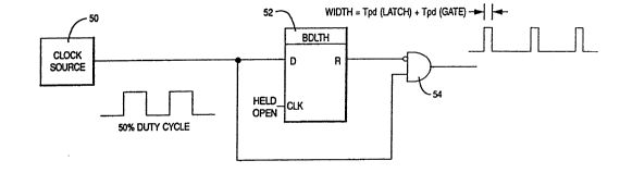
Figure 5 shows a simple embodiment of a logic circuit for
generating sliver pulses. A clock source 50 is coupled to the
inputs of AND gate 54. A delay 52 is introduced between the clock
'
. .
,
. - , ~ ,
1~ 72896-25
source 50 and one input of the AND gate 54. This delay 52 can be
a latch 52 having its clock input held open. The example of
Figure 5 uses a 50% duty cycle from clock source 50 to the inputs
of AND gate 5~. Due to the delay, Tpd (latch), introduced by the
latch 52, a narrow sliver pulse having a width equalling Tpd
(latch) plus Tpd (gate) is generated as shown in Figure 5A. The
width of this sliver pulse can be made as narrow as physically
possible. However, it is physically difficult to propagate such a
narrow pulse in a VLSI design. The actual implementation should
attempt to match the sliver width to the latch propagation delay
Tpd .
The present invention utilizes the correlation factor
with respect to circuit parameters on VLSI chips. Correlation is
defined as how well two or more circuit parameters track each
other. It is a measure of a tendency for two or more random
varlables to be associated. For example, if the two delays of two
different state devices correlate 100% , then their respective
delays would be identical. If the delays have 0% correlation,
then there is no relationship whatsoever between them. The
correlation factor takes into account the fact that the
properties, e.g., Tpd(min and max), power consumption, etc. of
state devices similarly situated on a VLSI chip correspond closely
with other state devices spaced nearby. Thls correlation is due
to several factors, e.g., similar processing of the chip and the
similar nature of the material, i.e., the silicon parameters of
areas on the chlp do not vary much wlth those areas ln close
spatial proximity.
The correlative properties are taken advantage of by
A
.
1~ 72896-25
creatiny pulse generators on the VLSI design using state de~ices
which are nearby the state devices to be clocked. Because o~
this, sliver pulses can be generated which have a width
substantially identical to the propagation delay Tpd f closely
spaced state devices.
The pulse generator shown in Figure 5 creates sliver
widths W substantially equivalent to the propagation delay through
the latch 52. Therefore, as a worst case example, substituting
W=Tpd into equation 3 and setting W equal to zero in equation 2
results in the following equations 7 and 8:
MIN DLY ~ Thld + S Eq. (7)
MAX DLY s CYCL~ - S - TSu Tpd(
These equations assume that the sliver width W
correlates to the propagation delay of the state device thus
guaranteeing that the sliver pulse cannot be too narrow to
propagate through the VLSI design. The sliver width is therefore
always wide enough to guarantee a predictable MIN PATH.
Figure 6 shows an example of how the correlated sliver
latches can be implemented on a VLSI design chip 58. The chip 58
includes blocks 60, 62 and 64 of physically similar latches L on
the chîp 58. Further, each block 60, 62, and 64 includes a pulse
or sliver generator G formed by using one of the latches L. A
clock signal CLK is input to the chip 58 at pin 56 and propagates
to a distribution stage 5~. The distribution stage 59 splits the
clock signal into several signals and propagates each clock signal
to one of the blocks 60, 62, and 64. At each block, the sliver
generator G generates the narrow sliver pulses to operate the
latches L in each of the blocks.
13 72896-25
A comparison of the savings obtained using sliver
latches in lieu of master-slave flip flops is given below with
respect to the examples assuming a master flip-flop consumes two
uni~s of power and occupies two units of area; and a latch
consumes one unit of power and occupies one unit of area; a sliver
generator consumes one unit of power and occupies one unit of
area. It is possible that sliver latches be yrouped in clusters
of four, six or eight, with each cluster containing a single pulse
generator. It is noted, however, that the actual group size is an
arbitrary figure.
It is therefore seen that a cluster of four latches and
one sliver generator can produce four master-slave flip flops
while consuming only five units of area, i.e., five "cells". On
the other hand, because each master-slave flip flop requires two
latches thus consuming two units of area, a pure master-slave flip
flop design requires eight units of area to produce four master-
slave flip flops. Therefore, there is a fractional reduction of
"3/8ths" in the number of master-slave cells saved using a sliver
latch design.
ExamPle 1
If the total number of flip flop cells are known in a
design tthe total number of master-slave flip flop cells equals
the total number of master-slave flip flops times two), then the
total reduction in master-slave flip flop cells gained through the ;~
use of sliver latches can be determined. Assuming sliver latches
are in clusters of four, the savings in area over a pure flip flop
design is equal to:
Savings in cells 8 .375 (# of master-slave flip flop cells)
.~ ''
~ . - -
.
14 72896-25
Eq. (9)
If there are 1,000 master-slaves flip flops in a design,
then there are a total of 2,000 master-slaves flip flop cells.
Inserting the numbers into Eq. 9 shows a saving of 750 cells.
Exam~le 2
Assuming all sliver latches are now grouped in clusters
of eight, the fractional savings over a pure master-slave flip
flop design is equivalent to "7/16th". If there are 1,000 master-
slave flip ~lops in design, then there are 2,000 master-slave flip
flop cells. Inserting the number into Eq. (10) below results in a
savings of 876 cells.
Savings in cells = .4375 (# of master-slave flip flop cells)
Eq. (10)
Example 3
Assuming a particular VLSI design having a total usable
area of 3,000 cells, but with only 700 master-slave flip flops,
then the power and cell savings achieved by using sliver latches
can be determined. The sliver latches are assumed to be available
in clusters of four only.
Because there are 700 master-slave flip flops, then
there are 1,400 cells allocated to the state devices. The number
of cells used by the sliver latches is computed as follows:
(1,400 cells) x (1 - .375) = 875 cells.
The cell savings can then be computed as follows:
3000 Total cells
- 1400 Master-slave _liP-flo~ cells
1600 Non-state device cells
1600 Non-state device cells
+ 875 Sliver cells
2475 Total cells with sliver latches
. .
.. . . . . .
..
.
.-. .: , . . ~: '
.
72896-25
3000 Total cells
- 2475 Total cells with sliver latches
525 cells saved.
The power saved can then be computed by determining the
"ce].ls saved ratio", since both the cell area and power
proportions are the same. The total power savings is thus given
by the equation:
3000 - 525
1 -3000 x 100 = 17.5% Power Savings
,:~
,,~
.
- . .
~' ',
.
, , . ~ .