Note: Descriptions are shown in the official language in which they were submitted.
~017719
This invention relates generally to a process for applying
spin-glass to a substrate, and more particularly to a process
for the planarization of semiconductor wafers. The invention
is especially applicable to inorganic spin-on glasses.
Spin-on glasses (SOG) are proprietary liquid solutions
containing siloxane or silicate based monomers diluted in
various kinds of solvents or alcohols. They are commonly
used for the planarization of semiconductor wafers, i. e. the
filling and levelling of the trenches formed between
interconnect paths deposited on the wafer. On coating and
curing of spin-on glasses, monomers are polymerized by
condensation and release of water, solvent, and alcohol. The
condensed material is a thin solid film having mechanical,
chemical and electrical properties which depend on the
starting solution, and the coating and curing process.
There are more than one hundred different SOG solutions
currently available. These are classified into two major
families:
1) Inorganic silicates.
2) Quasi inorganic siloxanes (methyl-siloxanes,
ethyl-, phenyl-, butyl-).
The various components of a SOG solution (silicon containing
oligomer, solvents mixture, and residual water) are in
equilibrium in the liquid phase. Immediately after coating,
volatile products (solvents and water) evaporate, and
polymerization occurs due to the formation by condensation of
silanol, Si-oH, bonds. These produce more water according to
the following reaction:
20~7719
,. ..
~ . . .
Si-o-H H H-o-Si- Si (H20) H-O-Si-
~ . . ~
O O O O O O
Si ~ O ~ Si-o-H + H-o-si --> si ~ o ~ si ~ o ~ si-
~ ~ . . . -
O O O O ~H20) 0 (H20) 0
Si ~ O ~ Si-O-H H-o-Si- Si ~ O ~ Si ~ O ~ Si-
~ . . .
Polymerization continues until the distance between
neighbouring silanol groups, Si-OH, becomes too large or when
too much by-product, such as water, blocks the condensation
reaction. Heating is then required to permit further
densification.
Both families of SOG solutions can incorporate boron or
phosphorus organometallic catalyst to improve the properties
of the films, such as: higher density, reduced hydrogen
content, higher coefficient of thermal expansion, better
flexibility and higher resistance to cracking. In the SOG
solution, the boron or phosphorus organometallic molecules
are generally not well bonded to the silicon-containing
compounds. Strong bonding generally occurs in the solid
state when the film is exposed to relatively high
temperatures. These organometallic molecules can
nevertheless polymerize in the solution to form poorly bonded
polymers that dissociate and form stable polymers during
coating and condensation of the film. As an example, a
Japanese SOG solution is alloyed with a phosphorus
organometallic molecule, PwOx(OH)y(OC2Hs)zl which is in
dynamic equilibrium with the solutions water and ethanol,
C2H50H:
~017719
~,"
H H
H ~ C ~ H H ~ C ~ H
H ~ C ~ H H ~ C ~ H H
~ . --
O H O 0
~ . . --
H ~ O ~ P : O + O ~ H ~ O ~ P : 0 + H ~ C ~ H
~ . . --
O H OH ~ C ~ H
H ~ C ~ H H H
H ~ C ~ H
H
If the ethanol C2H5OH, or water concentration suddenly drops,
as during coating and solvent evaporation, the equilibrium is
broken and, at high temperatures, the phosphorus
organometallic molecule will polymerize and connect to the
forming SioxHy film by producing more water and ethanol,
C2HsOH:
H H ~ O ~ Si- O ~ Si-
~ . .
O H H 0 O
~ . . . .
O : P ~ O ~ C ~ C ~ H + H ~ O ~ Si- O ~ Si ~
~ . . ~ --
0 H H O O
H H ~ O ~ Si O ~ Si
~ ~ O ~ H
Si 0 ~ Si
. . . H
~ O O H H
~ O : P ~ 0 ~ Si 0 ~ Si- + H ~ O ~ C ~ C ~ H
~ ~ ~ ~ -
O 0 O H H
. . . H
si- o ~ si-
~ ~ O ~ H
- - -
2017719
, ~ .
In theory, the phosphorus atom connects to the sio2 network
with three P-o-Si bonds. These bonds are formed by the
condensation of -P-OH or -P-OC2Hs, and -Si-OH. Water and
ethanol are formed as by-products and water must be
eliminated quickly to prevent reverse hydrolysis.
H H ~ O ~ Si O ~ Si H H ~ O ~ Si O ~ Si
~ ~ ~ . ~ ~ ~ .
0 0 0 0 0 0
~ . ~ ~ ~ ~ --
0: P ~ O ~ si- o ~ si- ~ o: P ~ o ~ si- o ~ si-
~ . . . . --
O O O O O O
15 H . . . . . .
~ Si O ~ Si H H ~ O Si O ~ Si
O ~ H
This reverse hydrolysis is extremely undesirable because it
contributes to the incorporation of hydrogen and inhibits the
action of the phosphorus organometallic catalyst.
Residual hydrogen forms silanol groups, SioH. It is very
difficult to remove and causes serious yield and reliability
problems. If this reverse hydrolysis continues, it is
possible to totally disconnect the phosphorus by forming many
different acids: hypo-phosphorus acid, H3P02; meta-phosphorus
acid, HP02; pyro-phosphorus acid, H4P20s; ortho-phosphorus
acid, H3P03; hypo-phosphoric acid, H4P206; meta-phosphoric
acid, HP03; pyro-phosphoric acid, H4P207; and ortho-
phosphoric acid, H3P04. As an example, the formation of
ortho-phosphoric, H3P04, due to reverse hydrolysis by
residual or ambient moisture, is:
2~17719
.....
H H ~ O ~ Si- H H ~ o ~ Si ~ O ~ Si-
~ . ~ . .
0 o O o O
O : P ~ O ~ Si ~ O : P ~ O ~ H + H ~ O ~ Si ~ O ~ Si
~ H
o ~ o o o o
lo ~ H ~ o
H H ~ o ~ Si- H H ~ o ~ Si ~ o ~ Si-
The acids that are formed corrode aluminum interconnects.
Consequently, for planarization over aluminum interconnects,
when maximum temperature is limited to about 450~C or so,
serious problems are encountered with film quality and
reliability.
These effects are not observed in the planarization of
dielectrics over refractory materials, such as polysilicon,
silicides and refractory metals, that allow very high
temperature curing (over 800~C) due to more complete
thermally induced condensation of pairs of silanol bonds, Si-
OH, over long distances. This type of planarization overrefractory materials is relatively easy.
The difficulty of using silicate SOGs for the planarization
of low-melting point materials, such as aluminum has caused a
worldwide trend not to use purely inorganic silicate
(including phosphosilicate) SOGs and to use instead members
of the quasi-inorganic siloxane family. However, there are
significant disadvantages in using quasi-inorganic SOGs
relating to their electrical properties, and their use is
becoming uncertain and questionable for advanced
applications.
A further problem is caused by the absorption of water during
curing. SOGs, particularly phosphorus alloyed SOGs, are
extremely hygroscopic materials, and rapidly absorb ambient
moisture during curing. This moisture pick-up promotes the
7 ~ ~
. .~
irreversible reactions described above, and the resulting
SOG films have poor properties and reliability.
An object of the invention is to alleviate the
aforementioned problems by permitting the obtention of
higher quality inorganic SOG films over aluminum or other
materials that cannot tolerate high temperature processing.
According to the present invention there is provided a
method of planarizing a semiconductor wafer having
interconnect tracks of non-refractory material formed
thereon, comprising the steps of:
(i) applying a layer of inorganic phosphorus-based
spin-on glass to the wafer in a coating and spinning
chamber in the absence of moisture;
(ii) transferring the wafer in the absence of moisture
to a curing station;
(iii) curing the spin-on glass at a temperature in the
range of at least about 80~C. and not more than 450~C. in
the absence of moisture at said curing station to form an
SiO2 lattice connected to phosphorus atoms;
(iv) returning the wafer to the coating and spinning
chamber and repeating steps (i) to (iii) until a sufficient
film thickness has been achieved without in the interim
exposing the wafer to moisture so as to minimize reverse
~t.
~,
~ ~ ~ 7 7 ~ 9
,.~,.,
~, .,
hydrolysis during a planarization process and thereby
prevent irreversible reactions that form phosphorus acids
and thus lead to disconnection of the phosphorus atoms from
the SiO2 lattice.
The non-refractory materials may also be, for example,
Titanium, Titanium nitride, Titanium - Tungsten, Tungsten,
or a combination thereof.
By eliminating the moisture from the curing process, a
dense, low hydrogen content, high coefficient of thermal
expansion, flexible, crack-resistant and corrosion-free SOG
film can be produced.
After deposition of the first layer of dielectric, the
spin-on glass coating/cure process is preferably carried
out with a dedicated SOG processor, typically in the
following manner, which is described with reference to the
planarization of a series of semiconductor wafers:
a) The wafer is transported from sending cassette to a
coating chamber.
b) A few ml of a SOG solution are dispensed at the centre
of the wafer to be planarized.
c) The wafer is spun at a given RPM to spread uniformly
the
- 6a -
, ~.
20~7719
"
solution and to permit the evaporation of volatile compounds
and film solidification.
d) For SOG curing, the wafer is sequentially transported to
in-line hot plates which are temperature controlled at
temperature roughly between 80~C and 250~C.
e) The wafer is slightly cooled at an idle station.
f) The wafer is stored and cooled in a receiving cassette.
g) When all the wafers are received in the ambient exposed
receiving cassette, they are all together transferred to the
sending cassette for a second coat (steps a to f are
repeated). When all the wafers are received in receiving
cassette, they are all together transferred to the sending
cassette for a third coat (steps a to f are again repeated).
h) When sufficient coats have been applied, the wafers are
transferred to the station for the next process step.
During steps a) to g), an operation lasting about two hours,
the wafers are not exposed to ambient atmosphere and, unlike
the prior art, are maintained in a moisture-free environment.
As a result, the SOG films, particularly phosphorus alloyed
SOG films, cannot therefore absorb ambient moisture and
extremely high quality films are produced.
The invention also relates to an apparatus for applying spin-
on glass (SOG) to a substrate over low-melting point, non-
refractory materials such as aluminum, which provides a
moisture-free environment for the application of said spin-on
glass to minimize reverse hydrolysis during curing.
The invention will now be described in more detail, by way of
example only, with reference to the accompanying drawings in
which:-
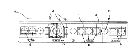
Figures la and lb show repectively plan and side views of aSOG planarization apparatus for carrying out the process
according to the present invention; and
-- 7 --
Figure 2 is a plot of the stress in a SOG film plotted
against relative humidity.
SOG processing equipment for coating and in-line curing of
the SOG film is relatively new. Prior art SOG processors do
not allow wafer manipulations, SOG coating, in-line curing,
cooling and storage under continuously controlled ambient
stations.
These now essential in-line ambient controlled stations are
provided in the SOG processor shown in Figure 1. Referring
now to Figure 1, the SOG processor comprises a main unit 1
defining a pularity of processing stations. The unit
includes sending cassettes 4, transport mechAnisms 2, in-line
cure plates 6 (up to 9), and receiving cassettes 7. The unit
1 further has a coating area 5 and cooling area 3.
More particualrly , the SOG processor comprises the following
elements:
1) One or more sending cassettes 4 to store the wafers to be
processed.
2) Transport mech~nism 2 to transfer, one by one, the wafers
from the sending cassette to the coating area.
3) Coating area 5 where the SOG coating and wafer spinning
is done.
4) Transport m~c-hAnism 2 to transfer the coated wafer from
the coating area to the first in-line temperature controlled
hot plate.
5) A first in-line hot plate area 6.
6) Transport mechAnism 2 to transfer the wafer from the one
in-line hot plate to the next.
7) A last in-line hot plate area 9.
8) A transport mec-h~ni~m to transfer the wafer from the last
in-line hot plate to a wafer cooling area.
9) A wafer cooling area 3.
10) A transport mec~hAnism to transfer the wafer from the
~,~
~0~7719
'.~.,
wafer cooling area to a receiving cassette area.
11) One or more receiving cassettes 7 to store the wafers
that received the first SOG coat.
The entire processor is provided in an inert environment.
The inert gas ambient protects the wafer at locations 1 to
11. The inert gas is typically nitrogen, but can be argon or
any other noble gas or any other non-reactive moisture-free
gas. This gas prevents reverse hydrolysis and permits the
production of films with considerably improved properties.
In order to determine the effects of moisture on film
properties, various SOG films were prepared using the
apparatus shown in Figure 1. The results are shown in Figure
2. Film stress was monitored for films processed under
uncontrolled atmospheric ambient and correlated with relative
humidity to show its effect on film properties.
Moisture pick-up and reverse hydrolysis pushes SOG film
stress toward compression (less tensile) because of an
internal volumetric expansion due to the formation of
silanol, Si-oH~ pairs from more compact si-o-si bonds.
The water pick-up effect is shown in Figure 2, which shows
that the equilibrium SOG mechanical stress is mainly
controlled by relative humidity. The compressive stress
effect due to the formation of silanol pairs is effectively
observed; the higher the relative humidity, the lower the
tensile stress.
Since the ambient conditions such as dew point, relative
humidity, and duration of the ambient exposure are not
constant from wafer to wafer and day to day, the resulting
films properties fluctuate and manufacturing is difficult.
While the invention is mainly applicable to inorganic SOGs,
it can be applied with success to quasi-inorganic SOGs.
~ ~ ~ 7 7 ~ ~
Either type can be alloyed or not with phosphorus, boron,
arsenic or lead. The benefits of the invention are more
noticeable with alloyed SOGs, but, since a non-alloyed SOG is
also extremely hygroscopic, the technique also apply to
unalloyed SOGs.
The number of coats can vary. Generally speaking, the hig~er
the number of coats, the better the end results.
The in-line high temperature hot plates can be replaced by an
in-line oven, an in-line plasma cure device, an in-line
microwave device, or an in-line ozone device, or an in-line
UV-ozone device, to permit cure in a moisture-free gas.
This inert gas it typically nitrogen, but can be argon or
another noble gas, any other moisture free gas, or a mixture
thereof. It can be heated or at room temperature.
The inert gas ambient can also be replaced by vacuum which is
also a moisture-free environment. The gas can be ionized
(plasma) or not.
The equipment described is an in-line one-wafer-at-a- time
processor but the invention also extends to single wafer or
batch systems where the SOG can be applied by spin coating,
immersion, spraying or other t~hniques that can be used to
apply the SOG film to a substrate in which the environment is
controlled.
-- 1 0
~.,