Note: Descriptions are shown in the official language in which they were submitted.
2~179~4
.~
HIGH FREQUENCY AMP~IFIER CIRCUIT CAPAB~E
OF OPTIMIZING A TOTA~ POWER CO~SUMPTION
. Background of the Invention~
_ _ .
j This invention relates to a high frequency
amplifier circuit for producing an amplified output
signal with automatic level control ~ALC). The
5 amplifier circuit is typically a radio frequency
~ amplifier circuit and is particularly useful in a
;~ portable radio communication deviae.
The amplifier circuit comprises a high frequency
output amplifier supplied with a bias voltage for
10 amplifying an amplifier input signal into a circuit
, output signal which is the above-mentioned amplified
output signal and is automatic level controlled in the
~3 manner which will presently be described. A high
frequency input amplifier device is connected to the
; 15 output amplifier and is for amplifying a circuit input
signal into an intermediate amplified signal to deliver
the intermediate amplified signal to the output
amplifier as the amplifier input signal. Supplied with
.,
j ..
;~
.:
.~ .
'' '
`.,~
20~7~a~
the circuit output signal back from the output
amplifier, the input amplifier device makes the circuit
output signal have a predetermined output level. In
this manner, the automatic level control i5 carried out
5 in the amplifier circuit comprising the input amplifier
- device and the output amplifier.
It is to be noted here that the circuit input
, signal has a variable input level. The amplifier input
; signal of the output amplifier has a gain controlled
10 level. The input amplifier device may consist of a
single high frequency input amplifier for producing the
, .,
-~ intermediate amplified signal. Alternatively, the input
amplifier device may additionally comprise at least one
high requency intermediate amplifier connected to the
15 input amplifier to produce the intermediate amplified
signal for delivery to the output ampliier.
The ampliier clrcuit 1~ naturally put into
, operation by electric power. When used in a portable
` radio communication device, the amplifier circuit is
20 ~upplied with the electric power usually from a battery
unit. The input amplifier device is supplied with a
` portion of the electric power as an input amplifier
power. The output amplifier is supplied with another
portion of the electric power as an output amplifier
- 25 power. The amplifier circuit is kept in operation with
a total power consumption of the electric power and is
supplied with the electric power with a certain supply
current value.
~ ,
~:-
$
, ,
201790~
The power consumption should be kept as littleas possible. It is therefore desirable to make the
total power consumption have an optimum value. This can
, be achieved by making each of the input amplifier device
`^ S and the output amplifier include a bias voltage control
circuit. Use of such bias control circuits is, however,
objectionable because the ampliier cirauit becomes
expensive.
Summar~ of the Invention:
It is therefore an object of this invention to
~, provide a high fre~uency amplifier circuit which is
capable of optimizing a total power consumption.
It is another object of this invention to
provide a high frequency amplifier circuit of the type
15 described which is not expensive.
Other objects of this invention will become
~i clear as the description proceed~.
On describing the gist of this invention, it is
possible to understand that a high frequency amplifier
20 circuit comprises an output amplifier supplied with an
' output amplifier power and with a bias voltage for
amplifying an amplifier input signal into a circuit
output signal having an output level, input amplifier
" means connected to the output amplifier and supplied
25 with an input amplifier power for amplifying a circuit
input signal into an intermediate amplified signal to
' deliver the intermediate amplified signal to the output
, amplifier as the amplifier input signal and supplied
:,
.,
. .
. ,
r
2~17904
with the circuit output signal for making the circuit
~, output signal have a predetermined level. The input and
, the output amplifier power is herein collectively called
' a total electric power with a supply current value
5 variable dependent on a total power consumption in the
input amplifier means and the output amplifier.
s Accordlng to thls invention, the above understood hlgh
frequency amplifier circuit is characterized by a
; current detection circuit supplied with the total
' 10 electric power for detecting the supply current value to
produce a current detection signal representative of the
supply current value, and a bia~ voltage control circuit
connected to the current detection circuit and the
output amplifier for controlling the bias voltage in
15 response to the current detection signal to make the
total power consumption have an optimum value.
Brief Description of the Drawing~
Fig. 1 is a block diagram of a conventional high
fre~uency amplifier circuit;
Fig. 2 is a block diagram of a high frequency
amplifier circuit according to a first embodiment of
this invention;
Fig. 3 is a graphical representation for use in
' describing first and second supply current values in an
25 input amplifier device and an output amplifier shown in
Fig. 2;
Fig. 4 is a graphical representation for use in
describing a current characteristic of a supply current
~j
`:
.,. .
. ' .
~.~
,:
2~179~
s
.,
value in the high frequency amplifier circuit shown in
Fig. 2;
Fig. 5 is a graphical representation for use in
describing another current characteristic of a supply
5 current value in the high frequency amplifier circuit
', shown in Fig. 2;
Fig, 6 is a block diagram of a high frequency
amplifier circuit acaording to a seaond embodiment of
thi~ invention
; 10 Fig. 7 is a block diagram of a high frequency
amplifier circuit according to a third embodiment of
7 this invention;
~' Fig. 8 shows a partial circuit arrangement which
is suitable for the high frequency amplifier circuit
lS illustrated in Fig. 7;
Fig. 9 illustrates signal waveforms for use in
describing operation of the circuit arrangement
illustrated in Fig. 8 ~ and
Fig. 10 illu~trates signal waveforms for use in
20 describing operation of the circuit arrangement
illustrated in Fig. 8.
' Description of the Preferred Embodiment:
Referring to Fig. 1, a conventional high
frequency amplifier circuit will be described at first
~'5 25 in order to facilitate an understanding of the present
s invention. The amplifier circuit is typically a radio
' frequency amplifier circuit and is particularly useful
in a portable radio communication device. The amplifier
`s
, .,~ ,
;
..... .
,
...
2~79~4
; circuit amplifies a circuit input signal IN into an
amplified output signal having an output level.
The amplifier circuit comprises a high frequency
output amplifier 21 which comprises an output FET (field
S effect transistor) 21a supplied with a bias voltage Vgc
of a constant level from a bias voltage supply unit (not
shown). The output amplifier 21 further comprises first
and second coupling capaaltors 21b and 21c and a choke
coil 21d. The output amplifier 21 is for amplifying an
10 amplifier input signal into a circuit output signal
which is the above-mentioned amplified output signal and
which is automatic level controlled in the manner which
will shortly be described. A high frequency input
amplifier unit 22 i~ connected to the output amplifier
15 21 through the first coupling capacitor 21b and
comprises a high frequency input amplifier device 23
which comprises an input FET (not shown). As will later
be described, the input amplifier unit 22 servas as an
automatic level control IA~C~ circuit.
The input amplifier device 23 may consist of a
single high frequency input amplifier for amplifying the
circuit input signal IN into an intermediate amplified
signal to daliver the intermediate amplified signal to
the output amplifier 21 as the amplifier input signal.
25 Alternatively, the input amplifier device 23 may
additionally comprise at least one high frequency
intermediate amplifier connected to the input amplifier
.
.
2017~04
to produce the intermediate amplified signal for
delivery to the output amplifier 21.
The input amplifier unit 22 further comprises an
output level detection circuit 24 supplied with the
5 circuit output signal from the output amplifier 21. The
output level detection circuit 24 detects the circuit
output signal to produce a d.c. voltage as a level
detection signal repre9entative of the output level.
~' The level de~ection signal is sent to a comparator 25
10 which is supplied with a reference voltage signal of a
~? d.c. reference voltage Vs from a reference voltage
generator (not shown). The reference voltage signal is
~ used in giving a predetermined output level to the
'; circuit output signal. The comparator 25 compares the
15 level detection signal with the reference voltage signal
to produce a supply voltage control signal
representative of a result of comparison between the
level detection ~ignal and the reference voltage signal.
The supply voltage control signal has a control signal
;, 20 level. The supply voltage control signal is supplied to
a supply voltage controller 26 which is given a supply
voltage from a power supply unit (not shown). The
supply voltage is controlled by the supply voltage
control signal. The input amplifier device 23 is
~? 25 supplied with a controlled supply voltage from the
supply voltage controller 26 and makes the circuit
. output signal have the predetermined output level.
,
.
.
,, .
` 2~730~
,
' 8
It is to be noted here that the circuit input
signal has a variable input level. The amplifier input
' signal of the output amplifier 21 has a gain controlled
level.
The amplifier circuit is naturally put into
operation by electric power. When used in the portable
radio communication device, the ampllfier circuit is
~upplie~d with the electric power from a battery unit
used as the power supply unit. The input amplifier
10 device 23 i9 supplied with a portion of the electric
power as an input amplifier power through the supply
voltage controller 26. The output amplifier 21 is
supplied with another portion of the electric power as
an output amplifier power through the choke coil 21d.
15 The amplifier circuit is kept in operation with a total
-~ power consumption or the electric power and is supplied
with the electric power with a certain 9upply current
value. The total power con~umptian should be kept as
little as possible. It is therefore desirable to make
~ 20 the total power consumption have an optimum value.
.`r It is to be noted in this connection that the
x~ total power consumption is influenced by fluctuation of
....
the gain controlled level. However, no consideration is
si made about compensating for the fluctuation of the gain
25 controlled level. In other words, the output amplifier
21 can not compensate the fluctuation of the gain
controlled level because the output FET 21a is supplied
, with the bias voltage Vgc of the constant level. This
";
. .
, .
.
.
., .
~ 2917904
. ~ g
.~,
means that the output amplifier 21 wastes the output
amplifier power. Such a defect also applies to the
input amplifier device 23. Consequently, the amplifier
,~i circuit has a degraded power consumption efficiency.
. 5 The input FET and the output FET 21a have
transistor characteristics which are different from each
other. The power consumption efficiency of the
amplifier circuit i~ influencQd by the tran~istor
characteristics. In order to optimize the power
10 consumption efficiency, each of the input amplifier
device and the output amplifier should include a bias
voltage control circuit. Use of such bias control
circuit~ is, however, objectionable because the
amplifier circuit becomes expensive.
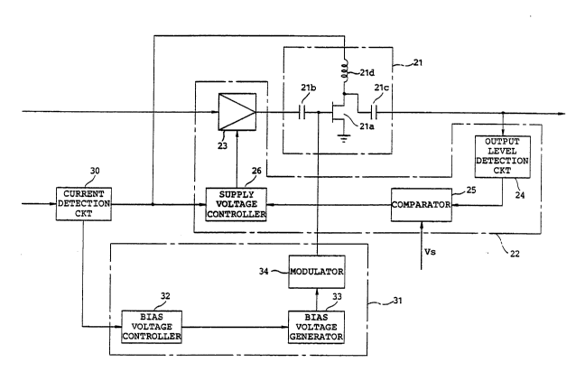
Referring to Pig. 2, the description will
proceed to a high frequency amplifier circuit according
to a first embodiment of this invention. The amplifier
circuit comprise~ similar parts de~ignated by like
reference numerals and additionally a current detection
20 circuit 30 and a bias voltage control circuit 31.
In Fig. 2, the amplifier circuit is kept in
operation with the total power consumption and is
supplied from the power supply unit with the electric
power with supply current having a certain phase
25 relative to the supply voltage and a certain supply
current value IS through the current detection circuit
30. The input amplifier device 23 is supplied with a
portion of the electric power as an input amplifier
.
~, , .
.
.. .
2Q17~0~
~ 10
,
power with a first supply current value ISl through the
supply voltage controller 26. The output amplifier 21
is supplied with another portion of the electric power
as an output amplifier power with a second supply
5 current value IS2. Supplied with electric power, the
current detection circuit 30 detects the supply current
to produce a current detection signal representative of
the pha~e of the supply ¢urrent and the supply current
value IS. A~ will presently be described more in
10 detail, the bias voltage control circuit 31 is for
r, controlling a bias voltage Vg in response to the current
~ detection signal to make the total power consumption
j have an optimum value.
Referring to Fig. 3, let the output level of the
15 circuit output signal is kept at the predetermined
output level by the automatic level control circuit a~
mentioned before. In the example being illustrated, the
first supply current value ISl decrea~e~ as the bias
voltage Vg increa8es. The second supply current value
~ 20 IS2 increases as the bias voltage Vg increases. The
'~J supply current value IS is a sum of the first and the
second supply current values ISl and IS2 and is defined
by a current characteristic CC shown by a dashed-line
curve. In this case, if the bias voltage Vg decreases,
~ 25 the output amplifier ~1 amplifies the intermediate
i~ amplified signal with a low gain because the second
supply current value IS2 decreases. However, the
; circuit input signal is amplified by the input amplifier
.
,11,, ~
., . - .
.,
,.
,
.; I
2~17~0~
, 11
device 23 with a high gain because the first supply
current value ISl is increased by the automatic level
control circuit. Namely, the first supply current value
ISl increases when the second supply current value IS2
5 decreases. It is to be noted here that the supply
current value IS becomes equal to a minimum value when
the output amplifier 21 is supplied with a speaific bias
voltage Vgl even though the output level is kept at the
predetermined output level. The specific bias voltage
10 Vgl is defined by the first and the second supply
current values ISl and IS2 which are equal to each
other. Under the circumstances, the bias voltage Vg
should be controlled by the bias voltage control circuit
' 31 in accordance with the current characteristic CC.
Referring to Fig. 4, the current characteristic
CC has a portion depicted in a left half of the current
characteristic CC and decreases with an increase in the
bias voltage Vg of the output amplifler 21. Another
portion is depicted in a right half of the current
20 characteristic CC and increases with the increase in the
bias voltage Vg. An extremum point is present between
the decreasing and the increasing portions. Let the
, bias voltage Vg be modulated into a modulated bias
voltage by amplitude modulation. In this event, the
25 supply current value IS varies dependent upon variation
of the modulated blas voltage~ For example, when the
output amplifier 21 is supplied with the modulated bias
voltage which i~ depicted at Vml and which i~ lower th~n
, '
12 2~7~0~
the specific bias voltage Vgl, the supply current is
i depicted at Il and has a first supply current value and
a first phase. Similarly, when the output amplifier 21
is supplied with the modulated bias voltage which is
5 depicted at Vm2 and which is higher than the specific
' bias voltage Vgl, the supply current is depicted at I2
: and has a -~econd supply current value and a second
phase. It is to be noted here that the ir~t phase
~ leads ~ radian relative to the second phase. The
; 10 current detection signal indicates leading and lagging
phases when the supply current has the supply current
values Il and I2. The supply current depicted at I3 has
a third supply current value which i9 much smaller than
the first and the second supply current values when the
15 output amplifier 21 is supplied with the modulated bias
voltage which is depicted at Vm3 and which is
~, substantially equal to the specific bias voltage Vgl.
~ Under the circum~tances, it will be under~tood that the
; total power consumption has the optimum value when the
20 output amplifier 21 is supplied with the modulated bias
voltage Vm3 because the third supply current value
becomes equal to a minimum value.
Turning back to Fig. 2, the bias voltage control
circuit 31 comprises a bias voltage controller 32, a
- 25 bias voltage generator 33, and a modulator 34. The bias
voltage controller 32 is supplied with the current
detection signal from the current detection circuit 30
and produces a bias voltage control signal having a bias
.
,
'
13 2a 17 9Q~
voltage control level dependent on the supply current
value IS. The bias voltage controller 32 comprises a
phase detector (not shown) for detecting the phase
,~ .
represented by the current detection signal. Operation
5 of the bias voltage controller 32 will now be described
strictly. By detecting the phase represented by the
aurrent detection signal, the bias voltage controller 32
decides whether the supply current value IS is in the
~' decreasing or the increasing portions of the current
, .......................................................................... .
4. 10 characteristic CC (Fig. 4). When the supply current
, value is in the decreasing portion, the bias voltage
controller 32 produces the bias voltage control signal
which serves to increase the bias voltage Vg up to the
specific bias voltage Vgl. On the contrary, the bias
15 voltage controller 32 produces the bias voltage control
signal which serves to decrease the bias voltage Vg down
~ to the specific voltage Vgl, when the supply current
;, value IS i9 in the increasing portion. In this manner,
the bias voltage controller 32 produces the bias voltage
20 control signal so that the supply current value IS
becomes equal to the minimum value.
` The bias voltage generator 33 generates a
` control voltage which is controlled by the bias voltage
control signal. The control voltage is supplied to the
25 modulator 34. As will later be described more in
detail, the modulator 34 comprises a pulse generator
(not shown) for generating a pulse signal and modulates
,~,
~ the control voltage into a modulated voltage by using
. .
.~
.
....
',
2~17~0~
14
the pulse signal. The modulator 34 supplies the
~ modulated voltage for use as the bias voltage to the
-~ output amplifier 21. Thus, the total power consumption
is kept at the optimum value.
A gallium-arsenide type FET may be used as the
output FET 21a. When the supply voltage is 6 volts
high, the input amplifier device 23 i8 given a constant
bias voltage of minu8 4 volts. The blas voltage Vg iR
, controlled between minus 1.5 volts and minus 4 voltR.
; 10 When the circuit input signal of 5 milliwatts reaches
the amplifier circuit, the circuit output signal should
be 30 dBm.
It should be noted in general that the battery
unit has a restricted voltage. The first supply current
15 value ISl is restricted to a predetermined value when
the output level of the circuit output signal should
keep a high level.
Referring to Fig. 5, let the irst supply
current value be restricted to the predetermined value
20 as exemplified at ISl'. The current characteristic
becomes different from that depicted in Fig. 3 and is
depicted as a different current characteristic CC'. The
current characteristic CC' represents the supply current
value which is a sum of the first and the second supply
25 current values ISl' and IS2. The current characteristic
~, CC' has a restricted portion deviated from a
corresponding portion of the current characteristic CC
thst ia shown ~y a d~shed line. en the first s~pply
..
.
: 2~1790~
current value ISl' is restricted, it is difficult to
keep the output level at the predetermined output level.
Moreover, if the bias voltage Vg is reduced down to a
prescribed bias voltage Vg2 which corresponds to a
supply current value Iva located between the restricted
portion and the decreasing portion of the current
characteristic CC', the bias voltage control circuit 31
may serve so as to reduce the bias voltage Vg. This
means that the bias voltage control circuit 31 falls
~,
10 into an uncontrollable state. This is because the bias
voltage control circuit 31 fails to discriminate the
-~ supply current value Iva in the restricted portian from
a supply current value Ivb in the increasing portion.
$~ Under the circumstances, the bias voltage Vg should be
15 kept at the prescribed voltage Vg2 when the first supply
` current value ISl' is restricted at the predetermined
value.
Referring to Fig~ 6~ the degcription Will
proceed to a high frequency amplifier circuit acaording
20 to a second embodiment of this invention. The amplifier
circuit is similar to the amplifier circuit illustrated
in Fig. 2 except that a bias voltage control circuit 40
,~ is used instead of the bias voltage control circuit 31.
The bias voltage control circuit 40 comprises a signal
25 level detection circuit 41 and a subsidiary control
circuit 42 in addition to the bias voltage controller
' 32, the bias voltage generator 33, and the modulator 34.
The bias voltage control circuit 40 keeps the bias
. '
..
. .
. ~ ., .
`
.
.'.~ `
2~179~
16
-~ voltage Vg at the prescribed bias voltage Vg2 when the
first supply current value ISl' is restricted to the
- predetermined value~. When the first supply current
value ISl' is restricted to the predetermined value, the
.J 5 comparator 25 produces the supply voltage control signal
having the control qignal level which is higher than a
predetermined control level to make the supply voltage
controller 26 supply the input amplifier device 23 with
the supply voltage of a maximum level.
10The signal level detection circuit 41 de~tects
-~ whether or not the control signal level is lower than
the predetermined control level. The signal level
detection circuit 41 delivers a detection signal to the
subsidiary control circuit 42 when the control signal
`, 15 level is not lower than the predetermined control level.
Supplied with the detection signal, the subsidiary
control circuit 42 stops supply of the bias voltage
control signal to the bias voltage generator 33 to keep
the bias voltage Vg at the prescribed bias voltage Vg2.
20 Namely, the bias voltage generator 33 supplies the
~ control voltage to the modulator 34 with a predetermined
r voltage on stop of the bias voltage control signal. The
modulator 34 modulates the control voltage into the
` modulated voltage for ~se as the prescribed bias voltage
25 Vg2. The detection signal may be supplied to the
modulator 34. In this event, the modulator 34 stops
modulation of the control voltage on reception of the
detection signal and produces the control voltage as it
.,
~,
.
, .
.,
2017~
17
stands for use as the prescribed bias voltage Vg2. If
the first supply current value ISl' is lower than the
predetermined value, namely, if the control signal level
is lower than the predetermined control level, operation
5 of the bias voltage control circuit 40 is similar to
that of the bias voltage control circuit 31.
Referring to Fig. 7, the descrlption will be
made as regard~ a high requency amplifier cirauit
according to a third embodiment of this invention. The
10 amplifier circuit is similar to the amplifier circuit
illustrated in Fig. 6 except that a bias voltage control
circuit 50 i8 used instead of the bias voltage control
circuit 40. The bias voltage control circuit 50
comprises a ratio detection circuit 51 instead of the
15 signal level detection circuit 41 illustrated in Fig. 6.
The ratio detection circuit 51 is supplied with the
supply voltage and the reference voltage.
It is to be noted here that the irst ~upply
current value ISl' is restricted when the comparator 25
20 is supplied with a high reference voltage in order to
increase the first supply current ISl', namely, in order
to keep the output level at a high level, although the
supply voltage is low. By detecting a ratio of the
reference voltage to the supply voltage, it is possible
25 to detect whether or not the first supply current value
ISl' is restricted.
Supplied with the supply voltage and the
reference voltage, the ratio detection circuit 51
., .
2017~0-4
18
I detects the ratio of the reference voltage to the supply
} voltage. The ratio detection circuit 51 delivers a
-' ratio detection signal to the su~sidiary control circuit
42 when the ratio is not higher than a predetermined
; 5 ratio. Supplied with the ratio detection signal, the
subsidiary control circuit 42 stops supply of the bias
voltage control signal to the bias voltage generator 33
to keep the bias voltagQ Vg at th0 pre~cribed bias
voltage Vg2. The bias voltage generator 33 supplies the
10 control voltage to the modulator 34 with the
predetermined voltage on stop of the bias voltage
control signal. The modulator 34 modulates the
predetermined voltage into the modulated voltage for use
as the prescribed bias voltage Vg2. If the ratio is
', 15 higher than the predetermined ratio, operation of the
bias voltage control circuit 50 is similar to that of
the bias voltage control circuit 40 illustrated in
Fig. 6.
Referring to Figs. 8, 9, and 10, the description
20 will proceed to a circuit arrangement which is suitable
for the high frequency amplifier circuit illustrated
with reference to Fig. 7.
In Fig. 8, the supply voltage controller 26
comprises a first operational amplifier OPl supplied
25 with the supply voltage control signal from the
comparator 25 through a non-inverting input terminal. A
first transistor TRl is connected to an output terminal
, of the first operational amplifier OPl. A second
,':
:.
.'~
., .
"~:
19 2~7~0~
-, transistor TR2 is supplied with the supply voltage
through the current detection circuit 30. In the manner
~, known in the art, the supply voltage controller 26
controls the supply voltage by the use of the supply
5 voltage control signal and supplies a controlled supply
voltage to the input amplifier device 23.
~ he current detection circuit 30 is supplied
with the eleatric power through a irst resistor Rl.
The first resistor Rl is u~ed in detecting a variation
10 which occurs in the supply voltage dependent on
variation of the supply current value IS. The supply
current value IS varies as illustrated in Fig. 9(a) when
the supply current value IS i9 in the decreasing portion
. of the current characteristic CC' shown in Fig. 5. The
15 supply current value IS varies as illustrated in Fig.
¦ 10~a) when the supply current value IS i9 in the
~ increasing portion of the current characteristic CC'.
s; It is to be noted here that the supply current value IS
shown in Fig. 9~a) has the phase which is different from
20 the phase of the supply current value IS shown in Fig.
~ 10~a).
r~ In Fig. 8, the variation of the supply voltage
, is detected at a point P1 through a first capacitor C1.
~ The first capacitor C1 i5 for detecting the variation of
`3~ 25 the supply current value IS as variation of a charged
~ voltage. sy the use of a second operational àmplifier
.~ .
~- OP2 connected to the first capacitor Cl through a second
resistor R2, the variation of the charged voltage is
~'
~.
:'
,'.~`
,.,
2~17~0~
amplified into an amplified voltage. The amplified
voltage is generated at a point P2 and is illustrated in
Figs. 9(b) and 10(b) to be supplied, as the current
detection signal, to the bias voltage controller 32.
5 The amplified voltage has an inverse phase relative to
the phase of the supply current value IS because the
j phase of the supply current 1~ inverted by the second
operational amplifier OP2. Thus, the current detection
circuit 30 detects the variation of the supply current
10 value in the form of the variation of the supply
voltage.
The bias voltage controller 32 comprises an
inverting amplifier AMl, first and second switching
circuits SWl and SW2, and an integrating amplifier AM2.
15 The inverting amplifier AMl is supplied with the
amplified voltage through a third resistor R3 and is
connected to the first switching circuit SWl. The
inverting amplifier AMl has an amplification actor
Y equal to unity and proauces an inverted voltage having
20 an inverted phase relative to the phase of the amplified
voltage. The inverted voltage is generated at a point
P3 and is illustrated in Figs. 9(c) and 10(c). The
, first switching circuit SWl is connected to the
inverting amplifier AMl and the integrating amplifier
25 AM2 and is control~ed by the pulse signal supplied from
the modulator 34 which will later be described. The
second switching circuit SW2 is connected to the second
operational amplifier OP2 and the integrating amplifier
.
.
~,:
.
,
21 2 ~ 1 7 ~ O L~
AM2 and is controlled by the pulse signal through a
first inverter IVl. As a result, the first switching
circuit SWl is turned on and turned off in synchronism
with the pulse signal when the supply current value IS
5 is in the decreasing portion of the current
characteristic CC'. The first switching circuit SWl
serves to qupply a positive-going full wave rectified
- waveorm o the amplifi~d voltage to the lntegrating
g amplifier AM2. The positive-going full wave rectified
10 waveform is generated at a point P4 and is illustrated
in Fig. 9(d).
The second switching circuit SW2 is turned on
:~ and turned off in synchronism with the pulse signal when
the supply current value IS is in the increasing portion
. 15 of the current characteristic CC'. The second switching
~3 circuit SW2 serves to supply a negative-going full wave
rectified waveform of the amplified voltage to the
integrating amplifier AM2. The negative-going full wave
^~ rectified waveform i9 generated at the point P4 is
20 illustrated in Fig. lO(d). The inverting amplifier AMl
and the first and the second switching circuits SWl and
SW2 may be collectively called a phase detector because
'~ the positive-going and the negative-going full wave
rectified waveforms are delivered in accordance with the
, 25 phase of the supply current.
~: When the supply current value IS is in the
. decreasing portion of the current characteristic CC',
the integrating amplifier AM2 integrates the
.
,~ .
:
- .
2~17~
22
positive-going full wave rectified waveform. The
integrating amplifier A~12 produces an integrated voltage
signal, as the bias voltage control signal. In the
manner depicted at Fig. 9(e), this integrated voltage
5 signal grows from a reference level Vr indicated by a
', dashed horizontal line and may herein be referred to as
an increasing voltage ~ignal. The lncreasing voltage
signal is generated at a point P5 and serves to raise
the bias voltage Vg up to the specific bias voltage Vgl.
10 On the other hand, the integrating amplifier AM2
integrates the negative-going full wave rectified
, waveform when the supply current value IS is in the
increasing portion of the current characteristic CC'.
The integrating amplifier AM2 produces another
15 integrated voltage signal, as the bias voltage control
signal. In the manner depicted at Fig. 10(e), later
integrated voltage signal decrea~es from the reference
level and may herein be reerred to as a decreasing
voltage signal. The decreasing voltage signal is
20 generated at the point P5 and serves to decrease the
~ bias voltage Vg down to the specific bias voltage Vgl.
i The ratio detection circuit 51 comprises a third
operational amplifier OP3 and a first voltage dividing
circuit 51a supplied with the supply voltage. The third
25 operational amplifier oP3 is supplied with the reference
voltage Vs and a divided supply voltage divided by the
first voltage dividing circuit 51a. As described
before, the ratio detection circuit 51 detects the ratio
23 2017~0~
of the reference voltage to the supply voltage and
delivers the ratio detection signal to the subsidiary
control circuit 42 when the ratio is not higher than the
predetermined ratio, namely, when the high reference
j 5 voltage is supplied to the comparator 25, although the
supply voltage is low.
The ~ubsidiary control circuit 42 comprises a
third switchin~ circult SW3 supplied with the bias
! voltage control signal and a second voltage dividing
10 circuit 42a supplied with a driving voltage Vdd.
i Supplied with the ratio detection signal, the third
~ switching circuit SW3 stops supply of the bias voltage
`j control signal to the bias voltage generator 33.
otherwise, the third switching circuit SW3 supplies a
15 divided driving voltage dlvided by the second voltage
dividing circuit 42a.
The bias voltage generator 33 comprises a fourth
operational amplifier OP4. The fourth operatlonal
ampliier OP4 converts one of the blas voltage control
20 signal and the divided driving voltage into a converted
voltage dependent on operation of the third switching
~ circuit SW3. The converted voltage is used as the
- control voltage.
The modulator 34 comprises a pulse generator 34a
25 and a differentiation circuit 34b comprising a fifth
~ operational amplifier OP5 supplied with the control
s voltage from the bias voltage generator 33. The pulse
generator 34a generates the pulse signal illustrate~ in
-
; .
.~ ~
2~7~0~
24
Figs. 9(f) and 10(f). The pulse signal is supplied to
an inverting input terminal of the differentiation
circuit 34b through a second inverter IV2. The
differentiation circuit 34b modulates the control
5 voltage with the pulse signal into the modulated signal
for use as the bias voltage Vg. At a point P6, the
modulated signal rises up to the speclfic bias voltage
Vgl rom the state shown in Flg. 9~g) when the supply
current value IS is in the decreasing portion of the
10 current characteristic CC'. On the other hand, the
modulated signal is decreased down to the specific bias
voltage Vgl from the state shown in Fig. 10(g) when the
supply current value IS is in the increasing portion of
the current characteristic CC'.
The pulse signal should have a frequency which
~ is lower than that of an information signal carried by
s the circuit input signal. When an audio 9ignal i9
carried by the circuit lnput signal, the pulse signal
should preferably have a frequency selected between 50
, 20 and 60 Hz.
s While this invention has thus far been described
~ in conjunction with a few embodiments thereof, it will
;~` readily possible for those skilled in the art to put
~ this invention into practice in various other manners.
-~ 25 For example, the pulse generator 34a may be placed in
-.:
the bias voltage controller 32 rather than in the
modulator 34. In this event, the pulse signal is
. . .
.
~ 25 2~17~0~
. supplied to the modulator 34 from the bias voltage
controller 32.
.'
'
"`' ' '