Note: Descriptions are shown in the official language in which they were submitted.
20179Z6
,,
SECOND ORDER ACTIVE FILT~R~
This invention relates to second order active filters.
It is well known to provide circuits with various filter characteristics for filtering
~ and phase correc~ng signals. With increasing complexity of electronic circuits, the design
-, 5 requiren~nts for filters are becoming increasingly stringent, and the filters can become
;, increasingly complex, costly, and diffieult to adjust or tune to achieve the particular desired
filter t~ansfer characteristic.
In addition, it is desirable to faeilitate the manufaeture of filters at low eost, by
;5 using to the largest possible extent eomponents whieh have standardized values and
; ,, 1 0 reladvely low toleranees, and by being able to follow a tuning praeedure whieh involves
5' only a single adjustment of eaeh parameter, rather than repeated and reeursive adjustments.
An objeet of this invendon, therefore, is to provide a seeond order aetive filter
, whieh ean have various types of filtereharaeteristie and whieh ean be tuned easily to meet
partieular requirernents.
1 5 According to one aspeet of this invention there is provided a filter comprising: an
input terminal, an output terrninal, and a cornmon terminal; a first reactance and a resistance
coupled in series between the input and common tesminals; a first amplifier having an input
.'5 coupled to a conneetion point between the first reactance and the resistanee and having an
output eoupled to the output terminal; a potendal divider eoupled between the output
-. 2 0 terminal and one of the input and co~on temlinals; a seeond amp}ifier having an input
, eoupled to a tapping point of the potential divider and having an output; and a seeond
reaetanee eoupled between the output of the seeond amplifier and the connection point;
wherein one of the reaetanees is induedve and the other is eapaeidve.
The invention pro~rides a family of f~lters with sueh a eonfiguration, different filter
2 5 eharaeterisdes being provided by different arrangements of the eomponents of the filter.
- In a ftrst form of the filter, the potenda1 divideris eoupled between the output
ter~mna1 and the common terminaL With such a form, the second reactance can complise a
capaeitanee. A low-pass filter is then provided if the ftrst reaetanoe eomprises an
induetanoe eoupled between the input terminal and the eonneelion point, and a band-pass
3 o filter is provided if the first reactanoe eompIises an induetance coupled between the
~:~ conneetion point and the common tenninaL Alternatively, the second reactanoe ean
comprise an inductance. A high-pass filter is then provided if the first reactance compIises
a capacitance coupled between the input tenninal and the connection point, and a band-pass
- filter is provided if the first reactanoe cornprises a capacitance coupled between the
3 5 connection point and the common terrninal. The filter can be made panicularly accurate by
including a capacitance coupled in series with the resistance of the potendal divider for
compensating for a resistance of the inductance which constitutes the second reactance.
.~.'` ~
, . .
;~-
,i
20179Z6
.
-, In ano~her fo rn of the fil~er, the potential divider is coupled between the inpu~
~- terminal and the oulput terminal. With such a forrn, a band-stop filter is provided if the first
reac~ance comprises an induc~ance or a capacitance coupled between the input terminal and
s the connec~ion point.
.~ .
According to another aspect this invention provides a filter comprising: an input
~, terrninal, an output terminal, and a common terminal; a first reactance and a resis~ance
coupled in series between the input and common terminals; a first amplifier having an inpu~
coupled to a connection point between the first reactance and the resistance and having an
output coupled îo the output tertninal; a first potendal divider coupled between the input
1 0 terminal and one of the output and common terminals; a second amplifier having an input
coupled to a tapping point of the first potential divider and having an output; a second
reactance coupled between the output of the second amplifier and the connection point; a
-' second potential divider coupled between the output terminal and the common terminal; a
, third amplifier having an inpu~ coupled to a tapping point of the second potential divider and
1 5 having an output; and a third reactance coupled between the output of the third amplifier and
A the connection point; wherein at least one of the reactances is inductive and at least one
other is capacitive.
A low-pass notch filter is provided if the first reactance comprises an inductance
coupled between the input terminal and the connection point, and the second and third
2 0 reactances comprise capacitances, or if the first reactance comprises a capacitance coup1ed
.- between the input terminal and the connection point, the second reactance comprises an
inductance, and the third reactance comprise a capacitance. A high-pass notch filter is
provided if the fLrst reactance comprises a capacitance coupled between ~he input terminal
and the connection point, and the second and third reactances comprise inductances. A
2 5 high-pass notch filter has a notch or band-stop characteristic with attenuation of lower
frequencies below the notch frequency, and conversely a low-pass no~ch fil~er has a no~ch
. or band-s~op charac~eristic wi~h attenuation of higher frequencies above the notch
frequency.
According to a further aspect of this invention there is provided a filter comprising:
3 0 an input terrninal, an output terminal, and a common tenninal; a first reactance and a
-:. resistance coupled in series between the input and common terrninals; a first amplifier
having an input coupled to a connection point between the first reactance and the resistance
, and having an output coupled to the output terminal; and at least one of: (i) a first potential
divider coupled between ~he input terrninal and one of ~he ou~put and common ~erminals, a
3 5 second amplifier having an input coupled to a tapping poin~ of ~he firs~ potential divider and
. having an OUtpltt, and a second reactance coupled between the output of the second
amplifier and the connection point; and (ii) a second potential divider coupled between the
output tem ina and the common terminal, a thrrd amplifier having an input coupltd to a
' , ' - .
.
,~ .
,.
.
20179Z6
, 3
, ~apping point of the second potential divider and having an output; and a third reactance
coupled between the output of the third amplifier and the connection point; wherein at least
-~ one of the reactances is inductive and at least one other is capacitive.
Any of the above filters may include an amplifier via which the potential divider is
t 5 coupled to the input terminal, the amplifier having an input coupled to the input terrninal and
an output coupled to the potential divider.
The invention will be further understood from the following description with
' reference to the accompanying drawings, in which:
Fig. I schematically illustrates a general form of filter in accordance with the, 10 invention;
Figs. 2 ;Ind 3 schematically illus~rate alternative forms of low-pass no~ch filter in
. accordance wi~h the invention;
Fig. 4 schematically illustrates a low-pass filter in accordance wi~h ~he invention;
Fig. S schematically illustrates a high-pass notch filter in accordance with the1 5 invention;
Fig. 6 schematically illustrates a high-pass filter in accordance with the inven~ion;
Figs. 7 and 8 schematically illustrate alternative forms of band-pass filter in
accordance with the invention;
Figs. 9 and 10 schematically illustra~e alternative forms of band-stop (notch) filter
2 0 in accordance with the invention; and
Figs. I l and 12 schematically illustrate alternative forms of all-~ass fil~er in
accordance with the invention.
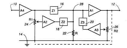
Referring to Fig. 1, there is illustrated therein a general form of filter in accordance
with this invention, the filter comprising an input terminal 10 for a signal to be filtered, an
2 5 output terminal 12 for a filtered signal, a common terminal 14 which is shown as being
grounded, amplifiers Al to A4, reactances 16, 18, and 20 having impedances Zl to Z3
,` respectively, a resistor 22 having a resistance R, and resistive potential dividers 24 and 26
having resistances Rl and R2 respectively. The amplifiers Al to A4 are conveniently unity
gain (over the entire bandwidth of the signal to be filtered) buffer amplifiers having a high
3 0 input impedance and a low output impedance. The amplifier A4 is not an essential part of
the filter itself but serves to isolate the remainder of the filter from preceding circuitry which
is connected to the input terminal 10; accordingly this amplifier is not discussed further
below.
.~ The reactance 16 and the resistor 22 are coupled in series between the input
.~ 35 terminal lO(viatheamplifierA4)andthecommonterminal 14. AsshowninFig. I,the
resistor 22 is closest to the common terminal 14, but as described further below the
positions of the reactar.ce 16 and the resistor 22 can be interchanged. The amplifier A I has
;
,.~
~.:
... .
20179Z6
an input connected to a connection point 28 between the reactance l 6 and the resistor 22
and an output connected to the output terminal 12.
As shown by solid line connections, the potential divider 24 is coupled between the
input terminal 10 (via the amplifier A4) and the cornmon terminal 14, and the amplifier A2
has an input connected to a tapping point of this potential divider 24 and an output coupled
via the reactance 18 to the connection point 28. Similarly, the potential divider 26 is
coupled between the output terminal 12 and the cotnmon terminal 14, and the amplifier A3
', has an input connected to a tapping point of this potential divider 26 and an output coupled
via the reactance 20 to the connection point 28. As described in futther detail below, either
1 0 the components 24, A2, and 18 or the components 26, A3, and 20 may be omitted to form
different configurations of the filter. In addition, as shown in Fig. I by a broken line, the
~` potential divider ~4 can be connected lo the output terminal 12 instead of to the common
tet~ninal 14, so that it is then couple between the input terminal 10 (via the amplifter A4)
and the output terminal 12.
1 5 The reactances 16, 18, and 20 can be inductive or capacitive, provided that at least
e one of them is inductive and at least another of them is capacitive, When ~he reactance 18 is
. present, its impedance Z2 is generally of the opposite nature to the impedance Zl of the
reactance 16, i.e. Z2 is inductive if Zl is capacitive, and Z1 is capacitive if Zl is inductive.
Although not shown in the drawings, it should be appreciated that the reactance 18
2 0 having the impedance Z2 can be constituted partly by a reactive component 18 connecled as
shown and partly by another reactive component of the sarne type (i.e. inductive if the
reactance 18 is inductive, or capacitive if the reactance 18 is capacitive) which is connected
in parallel with the reactance 16. Similarly, the reaclance 20 having the impedance Z3 can
be constitu~ed pattly by a reactive component 20 connected as shown and partly by another
, 2 5 reactive component of the same type which is connected in parallel with the resistor 22.
, Referring to Fig. 2, a low-pass notch filter is illustrated in which the impedances
Zl, Z2, and Z3 of Fig. 1 are constituted by an inductance L1, a capacitance Cl, and a
capacitance C2 respectively. In Fig. 2, tapping ratios m and n are also shown for the
potential dividers 24 and 26 respectively. For example, in the solid line configuMtion of
3 o Fig. 2, the resistance between the comrnon terminal 14 and the input of the amplifier A2 is
mR 1 and the resistance between the output of the amplifier A4 and the input of the amplifier
A2 is ( 1 - m)R 1 .
' The filter of Fig. 2, which can conveniently be used for an elliptic (Cauer) or an
inverted Chebyshev filter, has a transfer characteristic T(s) of the form
3 5 T(s) = (S2 + z2)/(s2 + (sp/Q) + p2), and thus is controlled by the three parameters z,
p, and Q. The parameter z is a zero fre~uency which is determined by the values Ll, Cl,
`~ and m. Thus in designing the filter of Fig. 2 the values L1 and Cl can be chosen as
standard values and the value of m adjusted or tuned to provide an exact desued value of
'
'
'.,~
20~7926
the notch frequency. The parameter p is a pole frequency which is deterrnined by the
values Ll, Cl, m in the case of the broken line configuration. and n. Thus having tuned m
as described above, the value of n can be adjusted or tuned to provide a desired pole
frequency p, without changing the zero frequency z. The pararneter Q is the quality factor
5 of the filter, which is determined by the above values and by the resistance R. Thus after
tuning m and n as described above, the value of the resistance R can be adjusted to provide
a desired value of Q, without changing the frequencies z and p.
The filter of Fig. 2 can, therefore, be easily tuned to provide a desired
characteris~ic.
1 0 The transfer charac~eristie of the filter ~f Fi~,. 2 ean be expressed b~/ the equation
T(s) = k(s2 + z2)/(s2 + (sp/Q) ~ p2), where z2 = I/(mLlCI). For the solid line
configuration of Fig. 2, p2 = I/(LI(CI + nC2)), Q = R~l((CI + nC2)/LI), and
k = mCI/(CI + nC2). For ~he broken line configuration of Fig. 2,
p2 = I/(LI(mCI + nC2)), Q = Rl((mC1 + nC2)/L1), and k = mCI/(mCl + nC2).
1 S Fig. 3 illustrates an altemative form of low-pass notch filter with a similar transfer
characteristic, again controlled by the three parameters z, p, and Q. In the filter of Fig. 3
the impedances Z1, Z2, and Z3 of Fig. 1 are consdtuted by a capacitance C1, an inductance
L1, and a capacitance C2 respectively, and the fapping ratios m and n are shown as in Fig.
2. As in the case of the fflter of Fig. 2, in designing the filter of Fig. 3 the values L1 and
2 0 C1 can be chosen as standard values and the value of m adjusted or tuned to provide an
exact dcsired value of the notch or zero frequency z, the value of n can the be adjusted or
tuned to provide a desired pole frequency p, without changing the zero frequency z, and the
value of the resistance R can then be adjusted to provide a desir~ed value of Q, without
changing the frequencies z and p. The filter of Fig. 3 can, therefore, also be easily tuned ~o
S provide a desired characteristic.
The transfer characteristic of the filter of Fig. 3 can also be expressed by theequation T(s) = k(s2 + z2)/(s2 + (sp/Q) + p2), where in this case z2 = rnJ(LlCl) and
k = Cl/(C1 + nC2). For the solid line configuration of Fig. 3, p2 = I/(Ll(C1 + nC2))
and Q - R~l((Cl + nC2)/L1). For the broken line configuration of Fig. 3,
3 0 p2 = m/(L1(C1 + nC2)) and Q = R~l(m(C1 + nC2)/L1).
Fig. 4 illustrates a low-pass filter. in which the components 24, A2, and 1~ of
Fig. 1 are omitted and the impedances Z1 and Z3 of Fig. 1 are constituted by an inductance
L and a capacitance C respectively. The transfer cha~.~cteristic of the filter of Fig. 4 can be
expressed ~y the equation T(s) = p2/(s2 + (sp/Q) + p2), where p2 = l/(nLC) and
3 5 Q = R~(nC/L). Thus this filter is also easily tuned by firstly selecting standard values of
L and C and adjusting n to provide a desired pole frequency p, and then adjusting the
resistance R to provide a desired quality factor Q without changing the value of p.
-~- 20179Z6
Referring to Fig. 5. a high-pass notch filter is illustrated in which the impedances
Zl, Z2, and Z3 of Fig. I are constituted by a capacitance C1, an inductance L1, and an
inductance L2 respectively. Fig. 5 also shows the tapping ratios m and n for the potential
dividers 24 and 26 respectively. The filter of Fig. 5 has the transfer characteristic
S T(s) = (S2 + z2)/(s2 + (sp/Q) + p2), where as discussed above the three parameters z,
p, and Q are respectively the zero frequency, pole frequency, and quality factor of the filter.
The values Ll and Cl can be chosen as standard values and the value of m adjusted or
tuned to provide an exact desired value of the notch or zero frequency z. The value of n can
then be adjusted or tuned to provide the desired pole frequency p, without changing the
1 0 zero frequency z. The value of the resistance R c~n then be adjus~ed to plovide a desired
value of Q, without changing the frequencies z and p. Thus the filter of Fig. S can also be
easily tuned to provide ~ desired characteristic. In the above equation for the transfer
characteristic of the filter ot Fig. 5, z2 = n~/(LlCI), p2 = (L2 + nLI)/(ClLlL2), and
Q = R'l(C1(L2 + nLl)/(LlL2)).
1 5 Fig. 6 illustrates a high-pass filter, in which the components 24, A2, and 18 of
Fig. I are omitted and the impedances Z1 and Z3 of Fig. l are constituted by a capacitance
C and an inductance L respectively. l he transfer characteristic of the filter of Fig. 6 can be
expressed by the equation T(s) = s2/(s2 + (sp/Q) + p2), where p2 = n/(LC) and
Q = R~l(nC/L). Thus this filter is also easily tuned by firstly selecting standard va1ues of
2 0 L and C and adjusting n to provide a desired pole fre~quency p, and then adjusting the
resistance R to provide a desired quality factor Q without changing the value of p.
Figs. 7 and 8 illustrate altemative forms of band-pass filter, in which the
components 24, A2, and 18 of Fig. 1 are omitted, and the posidons of the reactance 16
(Zl ) and the resistor 22 (R) are interchanged from those shown in Fi~. I . In Fig. 7, the
2 5 impedances Z1 and Z3 are constituted by an inductance L and a capacitance C respectively,
and the center frequency p of the pass band of the filter is given by the equation
p2 = 1/(nLC). In Fig. 8, the impedances Z1 and Z3 are constituted by a capacitance C and
an inductance L respectively, and the center frequency p of the pass band of the filter is
given by the equation p2 = n/(LC). In each case the transfer characteristic of the filter is
3 0 expressed by the equation T(s) = (splQ)/(s2 + (sp/Q) + p2), and (ignoring the capacitor
Cs in Fig. 8 and discussed below) the quality factor is expressed by the equation
Q = R~(nC/L). Thus this filter is also easily tuned by firstly selecting standard values of
L and C and adjusting n to provide a desired center frequency p, and then adjusting the
resistance R to provide a desired quality factor Q without changing the value of p.
3 5 Fig. 8 also illustrates a modification of the band-pass filter, in which compensation
is provided for the parasitic resistance of the inductance L and the output impedance of the
amplifier A3, which are assumed to have a combined resistance r. The compensation is
provided in the filter of Fig. 8 by an additional capacitance Cs, shown in dotted lines,
2017926
which is connecled in series with the resistance R and has a value given by the equation
Cs = L/(rR~. This modification enables a higher degree of accuracy to be achieved and/or
a lower quality factor, and hence cheaper, inductance to be used, without changing the
tuning procedure. However, in this modified arrangement the quality factor of the filter is
5 expressed by the modified equation Q = R~l(nC/L)/(l + rRC/L).
Figs. 9 and 10 illustrate alternat ve forms of band-stop or notch filter, in which the
components 26, A3, and 20 of Fig. I are omitted. In Fig. 9, the impedances Zl and Z2 of
Fig. 1 are constituted by an inductance L and a capacitance C respectively, and the zero
frequency ~ of the notch (or the center frequency of the stop band of the filter) is given by
1 0 ~he equadon z2 = I/(mL~). In Fig. 10, the impedances Zl and Z2 of Fig. 1 are
consti~uted by a capaci~ance C and an inductance L respectively, and the zero frequency z i~
given by the equation z2 = m/(LC). In each case the transfer characteristic of the filter is
expressed by the equation T(s) = (S2 + z2)/(s2 + (sz/Q) + z2), and the quality factor is
expressed by the equation Q = R~l(mC/L). Thus this filter is also easily tuned by firstly
1 5 selecting standard values of L and C and adjusting m to provide a desired zero frequency z,
and then adjusting the resistance R to provide a desired quality factor Q without changing
the value of z.
Although in the above filter arrangernents the potential dividers 24 and 26 are
described and illustrated as being constituted by variable ;esistors, it should of course be
2 0 appreciated that they may alternadvely be constituted by fixed resisto~;s having values to
provide the desired filter characteristics. In addition, although each of Figs. I to 10 shows
the buffer amplifier A4 as being present, as already mentioned this is not an essential part of
the filter itself and may be omitted in particular circumstances.
Fies. I l and 12 illustrate alternative fortns of all-pass filter circui~, which may be
2 5 used as frequency-dependen~ phase correction circuits. Each circuit includes a band-pass or
band~stop filter as described above, a potential divider comprising two resistors 34 having
the same resistance, and a differential amplifier 32 with a gain of 2 over the entire
bandwidth of the circuit. Each of hgs. 11 and 12 shows the buffer amplifier A4 separately
from the filter; again this buffer amplifier is opdonal and need not be present, and of course
3 0 in these circuit arrangements no buffer amplifier would be present in the filter itself.
In each all-pass filter circuit the above-mentioned potential divider is coupledbetween the input terminal 10 (via the buffer arnplifier A4 if it is present) and the common
terrninal 14, and has a tapping point connected to one input of the differential amplifier 32.
The filter has its output terminal 12 connected to the other input of the differential amplifier
3 5 32, whose output constitutes an output of the all-pass filter circuit. In the case of Fig. 11,
the filter is a band-pass filter as described above with reference to Fig. 7 or Fig. 8, and its
output terminal 12 is connected to the inverdng (-) input of the differential amplifier 32, the
potential divider tapping point being connected to the non-inverting (+) input of the
2~)17926
amplifier 32. In the case of Fig. 12, the filter is a band-stop filter as described above with
reference to Fig. 9 or Fig. 10, and its output tern~inal 12 is connected to the non-inverting
(+) input of the differential amplifier 32, the potential divider tapping point being connected
to ~he inverting (-) input of the amplifier 32. In each case the transfer characteristic of the
5 all-pass filter circuit is given by the equation
T(s) = (S2 (st/Q) + t2)/(s2 + (st/Q) + t2), where t is the center frequency p of the
band-pass filter or the zero frequency z of the band-stop or notch filter, and Q is the quality
factor of the filter.
Numerous modifications, variations, and adaptations may be made to the panicular1 0 embodiments of the invention described above without departing from the scope of the
invention as defined in the claims.