Note: Descriptions are shown in the official language in which they were submitted.
20~7929~
-
-- 1 --
RADIATION METER
FI~T-n OF '1'~; lNV~ LlON
This invention relates to the measurement of beta dose rate,
and more particularly to the measurement of beta dose rate
using silicon PIN diode detectors.
It is known to use silicon PIN ~io~s as radiation detectors
for X and/or gamma radiation, but such det~Lo s are not at
present used for the mea~..enL of beta radiation in the
presence of X and/or gamma radiation of comparable dose
rate. The existing proce~llre and apparatus used for X or
gamma dosimetry are not suitable for beta radiation
dosimetry.
SUMM~RY OF TED~ lNV~;N'l'lON
The main object of the invention is to provide an iL~ oved
radiation meter which is capable of measuring a beta
radiation dose rate in the presence of extremely short
wavelength electromagnetic radiation such as X and/or gamma
radiation.
The present invention in a preferred form is a radiation
meter comprising first and second radiation detectors, a
shield for each detector, the shield for the first detector
being constituted by a thin layer of con~n~ting material,
and the shield for the s~cond detector being constituted by
either a thin layer of conducting material and a relatively
thick layer of dielectric mat~ri~l or a thick layer of low
atomic nllmh~n conducting material. The thin conducting layer
over one detector shields that detector from electro~-~netic
interference while rinir-l ly shiel~in~ it from beta
radiation, while the thick layer over the second detector
. ~
2!~179Z9
..
also has at least one conducting component which shields it
from electromagnetic interference, but, in addition, the
greater total thickness significantly attenuates beta
radiation. ~he thick layer should be composed of low atomic
number materials. The responses of the two detectors will
be found to be virtually i~nticAl for X and gamma radiation
above, typically, approximately 50keV but will differ
significantly for beta radiation. In this ~ay beta
radiation dose rate can be measured in the presence of X and
gamma radiation.
Other objects and features of the invention will become
apparent from the description which follows by way of
example.
BRIEF DESCRIPTION OF THE DRAWINGS
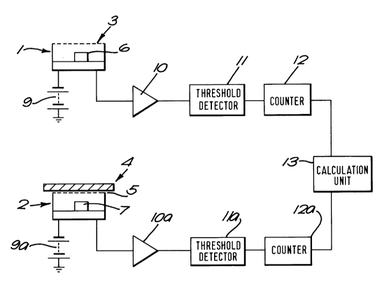
: Figure 1- shows schematicA lly the arrangement of twodetectors in a circuit suitable for implementing this
invention; and
Figure 2 shows one embodiment of a radiation meter
implementing the two detectors of the present invention.
DE~ATT~n DESCRIPTION
The particular embodiment described hereinafter is csn~ern~A
with measuring beta dose rate over an energy range of 0.5MeV
Emax to 2.27MeV Emax.
- As shown in Figure 1, two silicon PIN diodes 6 and 7,
operated in the reverse biased, non-conducting mode may be
used as the detecting elements in detectors 1 and 2
respectively. The detector 1 is csnn~cted to an ~mrlifi~r
10. The OULpuL of the amplifier is fed to a threshold
-
Z~)~79Z9
.
-- 3 --
detector 11 which provides an ouL~L pulse when the output
of the A~rl i fi~r ~re~c a threshold. The amplifier and
threshold detector may be adjusted for the purpose of
cAlihration. Output pulses from threshold detector 11 pass
S in turn to a counter 12 which is connected to one input of a
calculation unit 13. A battery 9 provides the Leve.-e bias
for the diode or the like in the detector 1 and the circuit
is completed by a supply rail (not shown).
The detector 2 is connected to an amplifier 10a. The output
of amplifier 10a is fed to a threshold detector lla which
operates in a si~ilAr-way to threshold detector 11 described
above. Output pulses from the threshold detector lla pass
in turn to a counter 12a which is connected to a second
lS input of the calculation unit 13. A battery 9a provides the
reverse bias for the diode or the like in the detector 2.
When mounted-for operation in an instrument neither detector
1 or 2 should be cove7ed by a significAnt thickness of high
atomic ntl~r materials in the casing or elsewhere; nor
should the sensitive layer in either of the detectors be
covered by glass.
One of the detectors 1 has the sensitive layer coveLed only
by a thin layer of electrically con~llctive material 3, which
is adequate to provide electrical scre~ning and which may be
for example, a copper-coated synthetic plastic. The
co~tlcting material shields the detector from
electromagnetic interference. The layer should be
sufficiently thin so as not to si~nifirAntly attenuate beta
radiation. A typical thickness may be of the order of
0.02mm.
201792g
-- 4 --
The other detector 2 is si~ rly covered with a thin layer
of electric~lly con~llctive material S (5imil~r to the layer
3) and is additionally covered with a substantially thick~r
layer of low atomic nllm~Pr material 4, which acts (as
described later) as an absorber and may, for example, be
plastic of the order of 2mm thick or magnesiur.. of the order
of l~m.. thick. Magnesium is one example of a metal which has
an atomic number less than 20.
The thic~ layer 4 should not be a complete attenuator of
beta radiation, but should allow some tr~ncmiicsion at high
el~e gies of beta radiation.
If a high energy source of beta radiation is considered, and
the response of a totally uncovered detector is defined as
F, where F is the count rate per unit dose rate, then the
re~onse of the detector 1 covered by the thin conducting
layer 3 will be kF, where k is the trAn-micsion of the
layer, and k will be close to unity: for example, O.9<k<1.
The response of detector 2 will be mF, where m is the
tr~ncmiicsion of the combined cover of the thin conducting
layer 5 plus the thicker layer 4, and m may be
a~ ~imately 0.5. The difference in response between the
two detectors in a high energy beta dose rate field will
thus be:
- kF - ~mF = (k-m)F, which may be of the order of 0.5F.
If a medium energy source of beta radiation is considered,
the response of a totally uncovered detector may be defined
as S, which will be less than F. The response of detector 1
cove~ed by this co~tlcting layer 3 will be nS, where n is
the tr~n micsion of the layer and is of the order of 0.5,
deter~in~ by the attenuation of the covering material,
which is itself det~rmine~ by the degree of i~mnnity to
2017929
-
-- 5 --
electric and magnetic fields which is required. Comparing
the two cases, n is not equal to k hecAll~e the elecLlon
energy is different in each case and hence the tr~ncmi~sion
is different. The response of detector 2 covered by the
conducting layer 5 and the layer 4 will be close to zero.
In this case the difference in count rate between the two
detectors will be:
nS - 0 = nS
The thic~n~-s of the layer 4 is selected to compensate for
the attenuation of -the necessary thin conducting cover at
medium energies of beta radiation, and to provide a
difference in response between the two detectors at high
energies of beta radiation which is a~plo~imately equal to
the difference in response between the two detectors at
medium energies of beta radiation. In other words, the
: difference in count rate obt~in~ should be the same
irrespective of actual electron energy. That being so the
following result should hold:
(k-m)F ~ nS
The value of m can be calculated, for example, ~y measuring
the values of k and F for 90Sr/90Y beta radiation (Emax =
2.27MeV), and the values of n and S for 204Tl beta
radiation. This can then be collverLed into a value for the
thickness of the layer 4.
It will be found that the response of the two detectors will
be substantially identical for X and gamma radiation under
conditions of secondary electron eqllilihrium~ and therefore
it is possible to measure beta radiation dose rate for
medium and high energy beta emitters even though the
20179Z9
-
-- 6 --
radiation detectors might be in X and gamma radiation
fields, the sig~ific~nt factor being the difference between
the two count rates as a result of the attenuation of the
beta radiation.
Accordingly, the calculation unit shown in Figure 1, which
may be a mi~loprocessor for example, subtracts the value in
the counter for detector 2 from the value in the counter for
detector 1, and divides the results by the a~ iate
factor, either (k-m) or n, to generate a value of beta dose,
which is approximately indepPn~nt of energy for high and
~c~ m energy beta radiation. The values of (k-m) and of n
are known for the particular arrangement of detectors used.
In a possible embodiment of an ins~.~uent for use as a
radiation meter, such as shown in Figure 2, the two
detectors and the circuitry of Figure 1 may be con~in~
- within a case 20. The case itself may be arranged to be a
suitable absorber, such that a gap s provided in the case
to accommodate the detector 1 which is covered only by the
thin co~ncting layer 3, as shown.
The second detector 2 is posi~ion~ within the case such
that the case forms part of the layer 4 protecting the
diode. The diodes 6 and 7 on he~rs 8 may be type BPX65
with the glass window removed.
The amplifi~r~ threshold de~tector and counter for the full
response beta ch~nnel (i.e. the detector having only the
co~llctive shield) are located inside the case as in~icAted
sch~tic~lly at 21. The A~rlifier, threshold detector and
counter for the half response beta ch~nnel are also located
inside the case at 22, and a mic.opsocessor 23 is similarly
supported inside the case. A battery 24 provides the
~eve?se bias for the diodes within the radiation meter, and
2~7929
,.
a liquid crystal display 25 in~ic~tes the measured beta
radiation dose.
A clip 26 may be pro~ided on the case for att~c~-nt of the
meter to a coveLall pocket, for example, for ease of
carrying.