Note: Descriptions are shown in the official language in which they were submitted.
Z~18398
This invention relates to an additional signal
multiplexing device for multiplexing an additional
signal in a vertical overscanning area of a main signal,
for example, and an additional signal separation device
for separating the additional signal from the maln
signal on which the additional signal is superposed.
As ls well known in the art, in commercially
available television receivers, an overscanning area is
generally provided. That is, in a case where the whole
size of the display image plane created by television
signals is indicated by broken lines in Fig. 1, the
actual dlsplay area of the television receiver is set to
a slightly smaller size as shown by a solid line in
Fig. 1. Therefore, an image on the peripheral portion
of the entire display image plane area is omitted by the
overscanning operatlon.
The reason why the overscanning area is provlded ls
to prevent that the lmage plane is partly cut out by
variation in the television signal receiving condition
or the performance of the television receiver, thus
making the vlewers unpleasant.
However, in recent years, the performance of tele-
vislon receivers is enhanced and the operation thereof
becomes stable, and the overscanning rate of 8 % whlch
is normally set can be satlsfactorily attained with some
margin. As a result, it has been proposed to transmit
an additional signal by use of the overscanning area
:,
,;
. . ~ . , :
~ . , ':-,' . ~
201~3398
(refer to "STUDY ON TRANSMISSION SYSTEM FOR WIDE ASPECT
IMAGE" in the technical report of television instltute
on Nov. 29, 1988, for example).
That is, a televislon signal includes 482 effective
scanning lines for each frame in the vertical dlrection
(in practice, 483 scanning lines are provided, but since
one of them is used for multlplexed text broadcastlng,
482 scannlng lines can be effectively used), and 482 x
(8/100) = 38 of the scanning lines are used for
multlplexing new additional signals. Therefore, not the
televislon signal but the additional signal is super-
posed on 19 (=38/2) of the 38 scanning lines which lie
on each of the upper and lower portions of the lmage
plane.
The above additlonal signal may lnclude side panel
components for lncreasing the width of the lmage plane
(refer to "A Wide Screen EDTV" IEEE Transaction on
Consumer Electronics, Vol. 35, No. 3, P.133-P.141,
AUGUST 1989), high-definition components of the lumi-
nance signal Y and chrominance signal C (refer to
"Extended Deflnltlon TV Fully Compatible with Exlstlng
Standard" IEEE Transactions on Communications, Vol.
COM-32, No. 8, P.948-P.953, AUGUST 1984), and helper
signals for sequential scanning/conversion (refer to
"Encodlng for Compatibility and Recoverability in the
ACTV System" IEEE Transactions on Broadcasting,
Vol. BC-33, No. 4, P.116-P.123, DECEMBER 1987).
- . " ~.
:~ :
. , . : : .
.
-` 2018398
However, when the addltional signals are superposed
on all of the 19 scanning lines on each of the upper and
lower portlons of the image plane, no margln can be
taken for the overscanning in the vertical directlon.
As a result, when the central value in the vertical
deflection is deviated, the image plane may be partly
cut out as shown by a hatched portion in Flg. 2. In
this case, the partial cut~out of the lmage plane also
occurs when the vertical deflection amplitude is lowered
and the raster is slightly narrowed in the vertical
direction.
In view of the above fact, the number of scanning
lines on which the additional signals are multiplexed on
each of the upper and lower portions is limlted to about
7 ln the prior art so as to prevent the image plane from
being partly cut out even when the vertical deflection
center is deviated or the vertical deflection amplitude
is lowered.
This lnvention has been made by taking the above
fact into consideratlon, and an ob~ect of this inventlon
is to provlde an additlonal slgnal separatlon device and
an addltlonal slgnal multlplexlng slgnal ln whlch addl-
tlonal signals can be multlplexed on the entlre portlon
of the vertlcal overscanning area without incurring the
partial cut-out of the image plane due to deviation of
the vertical deflect~on center or reduction in the ver-
tical deflection amplltude.
.. ~ . . . .. .
. . .: , . ~ .. .. - :
-~ . :, . .
. " : . , ,. -~ .. ~ - .
. : ,.
~, . . , :~., : :
znls3s~
According to one aspect of the present invention,
there ls provided an additional signal multiplexing
device for multiplexing an additional signal on a tele-
vlsion main signal, comprising a main slgnal outputting
circuit for outputting a television main signal at a
field repetition rate; an additional signal outputting
circuit for inverting an additional slgnal for every
other field and outputting the addltional signal at the
fleld repetition rate; and multiplexing circuit for
multiplexing the television main signal output from the
main slgnal outputting circuit on the additional signal
output from the additional signal outputting circuit.
Another aspect of the present invention, there is
provided an additional signal separatlon devlce for
separatlng an additional signal from a multiplexed
signal which is constructed by the televislon main
slgnal obtained at a field repetltion rate and the addl-
tional signal whose phase is inverted for every other
field and which is obtained at the field repetltion
rate, comprlslng delay clrcult for delaylng the
multiplexed signal by one fleld; and addlng clrcult for
separatlng the additional signal by addlng lnput and
output slgnals of the delay clrcult together.
Thls lnventlon can be more fully understood from
the followlng detailed descrlptlon when taken ln con-
~unction wlth the accompanying drawlngs, in which:
Fig. 1 is a diagram illustrating the overscanning
.: :
-
: ~. :: :,,
-` 20183~8
area;
Fig. 2 is a diagram illustrating the partial cut-
out of an image plane occurring when the central value
of the vertical deflection is deviated;
Fig. 3 is a block diagram showing the construction
of one embodiment of an additlonal signal multiplexing
device according to this invention;
Fig. 4 is a block diagram showing the construction
of one embodiment of an additional signal separation
device according to thls inventlon;
Flgs. 5 to 7A and 7B are diagrams for illustration
of the operation of the addltional slgnal multiplexing
device shown in Fig. 3;
Fig. 8 ls a flowchart for illustration of the addi-
tional signal separation devlce shown ln Fig. 4;
Fig. 9 is a block diagram showing the construction
of another embodiment of an additional signal
multiplexlng device according to thls lnventlon;
Flg. 10 ls a block dlagram showing the construction
of another embodiment of an addltlonal slgnal separation
device accordlng to this lnvention; and
Flg. 11 is a diagram for illustration of the opera-
tion of the additional signal multiplexing davice shown
in Fig. 9.
There will now be described an embodiment of this
invention with reference to the accompanylng drawings.
Flg. 3 shows the constructlon of one embodlment of
:,, :,, :,
. . , . , , , - , - . . ~ .
-- ~. :,~ . . -, ,
-. , , ! , ... .
.. : . ~ ' : '' ' '~'' . . ., ''
- : - ', . : '
,~, ' : ' ' ''. ' ' ~ . , , ,'' ' :`
. ' ~
2018398
-- 6 --
an addltional signal multiplexing device according to
this invention. Likewise, Flg. 4 shows the construction
of one embodiment of an additlonal signal separation
devlce according to thls invention.
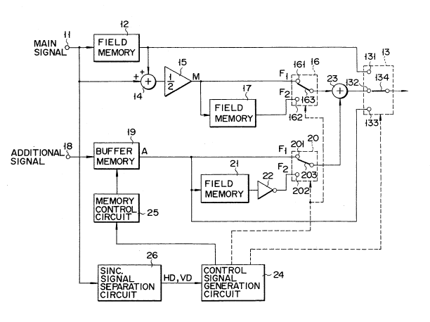
First, the additional slgnal multiplexing devlce
shown in Fig. 3 is explained. In Fig. 3, a reference
numeral 11 denotes an input terminal to which a main
signal is input. The main signal input to the input
terminal 11 is delayed by one field by means of a field
memory 12 and then supplied to a fixed terminal 131 of a
switch 13.
Input/output signals of the field memory 12 are
added together by an adder circuit 14 and the output of
the adder circuit 14 is multlplied by 1/2 by means of a
constant multipller circuit 15. As a result, an intra-
frame average of the main signal or the average value of
the main signal in the frame can be obtained. The main
signal M thus averaged in the frame is supplied to the
fixed terminal 161 of a switching circuit 16 and delayed
by one fleld by means of a field memory 17. The output
of the field memory 17 is supplied to a fixed terminal
162 of the switching circuit 16. A movable contact 163
of the switching circuit 16 is connected to the fixed
termlnal 161 in the first field Fl in the frame and to
the fixed terminal 162 in the second field F2.
A reference numeral 18 denotes an input terminal to
which an addltlonal signal ls lnput. The additional
. .
:. ` ': ,:` ~,. .
-:~ ' ` ' : : .:'
': ,.,
: . :
: ' ' ' ` ' :
:. , :
-- 2~1839~
-- 7
slgnal input to the input terminal 18 is written into a
buffer memory 19 and then read out at a preset timing.
The additional signal A read out from the buffer memory
19 is supplied to the flxed terminal 2~1 of a switching
circuit 20 and delayed by one field by means of a field
memory 21. The delayed output is phase-inverted by a
phase-inverting circuit 22 and then supplied to a fixed
terminal 202 of the switchlng circuit 20. A movable
contact 203 of the switching circuit 20 is connected to
the fixed terminal 201 in the first field Fl in the
frame and to the fixed terminal 202 in the second field
F2-
The selected output from the switching circuit 20
is added to the selected output from the switching cir-
cuit 16 by an adder circuit 23 and the output of the
adder clrcult 2~ is supplied to the fixed terminal 132
of a switching circult 13. A fixed terminal 133 of the
switching circuit 13 is supplied with the additional
signal A read out from the buffer memory 19.
Connection of a movable contact 134 of the
switching circuit 13 is controlled as described below.
Assume now that the effectlve scanning period i9
expressed by line numbers. Then, as shown by solld
lines in Fig. 5, the first field Fl ranges from 22 to
262, and as shown by broken lines in Fig. 5, the second
field F2 ranges from 285 to 525. Likewise, the
overscanning area ranges from 22 to 31 in the upper
.. ... ~ .
znls3ss
-- 8 --
portion of an image plane of the first field F1 and from
;'54 to 262 in the lower portlon of the image plane.
Further, the overscanning area ranges from 285 to 293 in
the upper portion of an image plane of the second field
F2 and from 516 to 525 in the lower portion of the image
plane.
With the above format, the movable contact 134 of
the switching circuit 13 is connected to the fixed ter-
minal 133 in the range from the top line of the lmage
plane to the seventh line (the llne numbers from 22 to
25 and from 285 to 287) for each frame and in the range
from the bottom line to the seventh line (the line num-
bers from 260 to 262 and from 522 to 525). Further, the
movable contact 134 of the swltching clrcuit 13 is con-
nected to the fixed terminal 132 ln the range from the
elghth llne from the upper end of the image plane to the
nineteenth line (the llne numbers from 26 to 31 and from
288 to 293) for each frame and in the range from the
eighth line from the lower end of the image plane to the
nineteenth llne (the line numbers from 254 to 259 and
from 516 to 521). The movable contact 134 of the
switching circuit 13 is connected to the fixed terminal
131 in the other range, that is, in a range other than
the overscanning area.
A control signal for controlling the switching
positlons of the switching circuits 13, 16 and 20 is
output from a control signal generation circuit 24. The
,, .. ~ :
~.:.
znls3ss
control slgnal generatlon clrcuit 24 also generates a
control slgnal for accesslng the buffer memory 19. The
operation of writing or reading the additional signal A
wlth respect to the buffer memory 19 ls controlled by a
memory control clrcuit 25 which ls driven by the above
control slgnal. Further, the control signal generatlon
clrcult 24 generates varlous control slgnals accordlng
to a horlzontal sync. slgnal HD or vertlcal sync. slgnal
VD separated from the maln slgnal by a sync. slgnal
separatlon circuit 26.
Now, the operation of the circuit with the above
constructlon is explalned with reference to Figs. 6, 7A
and 7B. Flg. 6 is a flowchart showlng the control
operatlon of the control slgnal generatlon clrcult 24
for controlllng the swltchlng clrcults 13, 16 and 20 and
the buffer memory 19. Further, Flgs. 7A and 7B are
dlagrams showlng an output of the switching clrcult 13.
As shown ln Flg. 6, it is checked ln the step Sl whether
the fleld ls the first fleld Fl or second fleld F2. If
it is determined that the field is the first field Fl,
the movable contacts 163 and 203 of the swltchlng clr-
cuits 16 and 20 are respectively connected to the fixed
terminals 161 and 201 in the step S2.
In the next step S3, it is checked whether or not
the llne number lies in the range of 22 to 31 or 254 to
262. If it ls determined that the line number lies ln
the above range, the additlonal signal A is read out
. .
;
- 2~)18398
-- 10 --
from the buffer memory 18 in the step S4. In the next
step S5, it is checked whether or not the line number
.Lies in the range of 22 to 25 or 260 to 262. If it is
determined that the line number lies in the above range,
S the movable contact 134 of the switching circuit 13 is
connected to the fixed terminal 133 in the next step S6.
As a result, as shown ln Flgs. 7A and 7B, the additional
signal A read out from the buffer memory 19 is output
from the switching circuit 13.
Further, lf lt is determined in the step S5 that
the line number does not lie in the above range, that
is, lf lt ls determlned that the llne number lles in the
range of 26 to 31 or 254 to 259, the movable contact 134
of the switching circuit 13 is connected to the flxed
15 termlnal 132 ln the step S7. In this case, as shown in
Figs. 7A and 7B, the sum signal of the main signal M and
addltional slgnal A ls output from the switchlng circuit
13.
Further, if it is determined in the step S 3 that
the line number does not lie ln the above range, that
is, if the llne number lies outside the vertical oversc-
anning area, the movable contact 134 of the switching
clrcult 13 is connected to the fixed terminal 131 in the
step Sg after the buffer memory 19 is set into the
wrlte-ln mode ln the step Sg. As a result, ln thls
case, the main slgnal supplled from the field memory 12
is output ~rom the switching circuit 13. The content of
... j, - , , - ~- -
. : . - .: . . - -
Z018398
the buffer memory 19 is re-written in the vertical blan-
king period, for example.
When it is determined in the step Sl that the field
is the second F2, the process is effected accordlng to
the steps Slo to S13. The process effected according to
the steps Slo to S13 is substantially the same as that
effected for the first field P1 according to the steps
S2 to Ss, and the explanatlon therefor is omitted.
As ls clearly understood from the above-
description, the addltlonal signal A read out from the
buffer memory 19 ls output from the switching circuit 16
in the range from the upper end of the image plane to
the seventh llne and from the lower end to the seventh
l~ne of each frame lrrespectlve that the field ls the
first field Fl or second field F2 as shown in Flgs. 7A
and 7B. Further, since the main signal M ls output at
the field repetition rate in the range from the eighth
line from the upper end to the nineteenth line and from
the eighth line from the lower end to the nineteenth
line for each frame and the additlonal slgnal A ls out-
put at the fleld repetltlon rate after the phase of the
additional signal A ls inverted in every other fleld, a
sum signal (M+Aj is output in the first fleld Fl and
a difference slgnal (M-A) ls output in the second field
F2. In a range other than the above range, that is, ln
an area other than the overscanning area, the maln
signal output from the field memory 12 is output.
. ~, . . .
. ,. ~ . .
' : : ' . : ,, .
~.. -. . ; `
-- Z018398
- 12 -
Next, the additional signal separation device shown
in Flg. 4 is explained. In Flg. 4, a reference numeral
31 denotes an input terminal to which a multiplexed
slgnal is input. The multiplexed signal input to the
S lnput terminal 31 is supplied to an output termlnal 33
via a switching circuit 32 when the movable contact 321
of the swltchlng clrcuit 32 is connected to a fixed ter-
mlnal 322. On the other hand, the multiplexed signal ls
supplled to the fixed termlnal 361 of a swltching cir-
cuit 36 after an inter-field difference or a dlfference
between the fields ls derlved by means of an inter-field
difference circult constructed by a field memory 34 and
an addltlon clrcult 35 when the movable contact 321 is
connected to the flxed termlnal 323. Further, when the
movable contact 321 ls connected to a flxed termlnal
324, the multiplexed signal is supplled to the fixed
terminal 362 of a swltchlng clrcuit 36 via the switching
circuit 32. The selected output of the swltching clr-
cult 36 is supplied to a buffer memory 37 via the
movable contact 363, stored therein output from the out-
put terminal 38.
Further, a reference numeral 39 denotes a sync.
signal reproducing clrcult for reproducing a horizontal
sync. signal HD and vertical sync. signal V~ in synchro-
nism wlth the multiplexed signal supplled to the inputtermlnal 31. A reference numeral 40 denotes a control
slgnal generatlon circuit for generating control signals
- . . .. ... ~ ,. ...
.,
. .
,
.
. -.
; .
Z0183~8
~or controlling the swltching positions of the switching
circults 32 and 36 and a control siynal for controlling
the access to the buffer memory 37 according to the
reproduced output from the sync. signal reproducing clr-
S cult 39. Further, a reference numeral 41 denotes amemory control circuit for controlling the
write-in/readout operation of the buffer memory 37
according to a control signal output from the control
slgnal generation circuit 40.
The operatlon of the circuit with the above
construction is explained with reference to Fig. 8.
Fig. 8 is a flowchart showing the control operation of
the control signal generation circuit 40 for controlling
the switching circuits 32 and 36 and buffer memory 37.
That is, it is checked in the step S21 whether or not
the llne number lles ln the range of 22 to 31, 254 to
262, 285 to 293 or 516 to 525. When the line number
lies in the above range, the buffer memory 37 is set
into the wrlte-in mode in the step S22. After this, it
is checked in the step S23 whether or not the line
number lies in the range of 22 to 25, 260 to 262, 285 to
287 or 522 to 525. When the line number lies in the
above range, the movable contacts 321 and 363 of the
swltching circuits 32 and 36 are respectively connected
to the flxed termlnals 324 and 362 ln the step S24. As
a result, as shown ln Figs. 7A and 7B, the additional
signal A lylng in the range from the upper end of the
- Z(~ 398
- 14 -
image plane to the seventh line and from the lower end
to the seventh llne for each frame is written into the
buffer memory 37.
If it is determined in the step S23 that the line
number does not lie in the above range, that is, if the
line number lies in the range of 26 to 31, 254 to 259,
288 to 293 or 516 to 521, the step S25 is effected to
connect the movable contacts 321 and 363 of the
switching circuits 32 and 36 to the fixed terminals 323
and 361. As a result, a difference between the sum
signal (M+A) in the flrst field Fl and the difference
signal (M-A) in the second field F2 shown in Figs. 7A
and 7B is derived by means of the field memory 34 and
addition circuit 35, thus reproducing the additional
signal A. The reproduced additional signal A is written
lnto the buffer memory 37 via the switching circuit 36.
If it is determined in the step S21 that the line
numbsr does not lie in the above range, the buffer
memory 37 is set into the readout mode in the step S26.
After this, in the step S27, the movable contact 321
of the switching circuit 32 is connected to the fixed
termlnal 322. As a result, the main signal lylng in an
area other than the vertical overscanning area is output
from the output terminal 33 via the switching circuit
32.
As described above, in this embodiment, the main
signal M is output at the field repetition rate and the
..
.. . .
` - 2~18398
additional signal A ls output at the field repetition
rate after the phase thereof is inverted in every other
field. Unlike the conventional case in which only the
main signal M is superposed in an area of the image
plane from the seventh line from the upper end to the
nlneteenth line and from the seventh line from the lower
end to the nineteenth line, the additional signal A is
also superposed in this embodiment. Therefore,
according to this embodiment, the additional signal A
can be multiplexed in the entire range of the vertical
scanning area wlthout incurring the partial cut-out of
the image plane due to deviation in the center of the
vertical deflection or reduction in the vertical deflec-
tlon amplltude. Further, ln this embodlment, slnce the
main signal M is output at the field repetltion rate and
the additional slgnal A ls output at the field repeti-
tlon rate after the phase of the additional signal A is
inverted in every other field, it is possible to easily
separate the additional signal A by taklng an inter-
field difference.
Further, in this embodiment, since the average ofthe main slgnal ln the frame derlved by means of a low~
pa99 filter constltuted by the fleld memory 12 and adder
circuit 14 ls used as the maln signal M, occurrence of
an unnatural image due to the fleld repetition ln the
moblle area Gan be prevented.
Flg. 9 shows the construction of another embodiment
,
..- .
,. . ~ .
- Z~1~33~8
- 16 -
of an additional signal multiplexing device according to
this invention. Likewise, Fig. 10 shows the construc-
tion of another embodiment of an additional slgnal
separatlon devlce accordlng to this inventlon.
In Flgs. 9 and 10, portlons whlch are the same as those
shown in Figs. 3 and 4 are denoted by the same refexence
numerals.
First, the additional signal multiplexlng devlce
shown in Fig. 9 ls explained. In the embodiment shown
in Flg. 3, the additional signal A read out from the
buffer memory 19 is multiplexed as it is. In contrast,
in this embodiment of Fig. 9, a line-difference deriving
circuit 51 and a line-sum deriving circuit 52 are con-
nected at the output stage of the buffer memory 19. As
shown in Fig. 11, the line-sum average output
(A2n_l+A2n)/2 output from the line-sum deriving clrcult
52 is multiplexed in the range from the upper end to the
sixth llne for each frame, the additlonal slgnal A13 of
the thirteenth line is multiplexed as it is via the
line-sum deriving circuit 52 in the seventh llne, and
the line-difference average output (A2n_l-A2n)/2 output
from the line-difference derlving circuit 51 is
multiplexed at the field repetition rate ln the range
from the eighth llne to the nlneteenth llne. In this
case, the readout operation of the buffer memory 19 is
effected so that the line-difference outputs for signals
on those lines which are the same as the lines
' . .
- 17 -
multiplexed on the first to the sixth llnes can be
multiplexed at the field repetition rate in the range
from the eighth line to the nineteenth line.
In the case of effectlng the above multiplexing
operation, the additional signals A2n_1 and A2n can be
reproduced by effecting the addition and subtraction
operations in a period of 8 H (1 H is one horizontal
scanning period).
That is, the additional signals A2n_l and A2n can
be reproduced by connecting a sum/difference deriving
circuit 61 at the output stage of the buffer memory 37
as shown in Fig. 10 and deriving the sum of and dif-
ference between two outputs which are read out from the
buffer memory 37 and are separated from each other by
8 H. However, the addltlonal signal A13 can be obtained
by outputting a readout output on the seventh line as it
ls .
Substantially the same multiplexing operation can
be effected for the lower portion of the image plane
although not explained in detail.
Wlth the above construction, the same effect as
that obtalned in the former embodlment can be obtained.
Further, since the line-difference outputs of the
addltional signals A are multiplexed in the range from
the eighth line from the upper end of the image plane to
the nlneteenth line and from the eighth line from the
lower end to the nineteenth line, the average power of
~ .. .
.
-
.
~n~3ss
- 18 -
the additional signals A to be multiplexed can be
reduced lf the additional signals A have the vertical
correlation. As a result, even if the image plane from
the eighth line to the nineteenth line is dlsplayed as
the result of deviation in the vertical deflection
center, visual influence by the additional signals A can
be suppressed.
Further, since addltional signals A for 13 lines
can be multiplexed on each of the upper and lower por-
tions of the image plane for each frame when the above-
described multiplexlng operation is effected, additional
signals A of the same amount as that in the former embo-
diment can be multiplexed.
Two embodlments of this invention have been
explained in detail. However, this invention is not
limited to the above two embodiments. For example, in
the embodiment of Fig. 3, the additional signals A are
multlplexed on the elghth line to the nineteenth line
from each of the upper end and lower end of the image
plane for each frame. However, the range in whlch the
additional signals A are multlplexed 19 not llmited to
the above range, and lt ls posslble to multiplex the
addltional slgnal A in the range in whlch the main
signal is superposed. Further, in the embodlment of
Fig. 3, the average slgnal M of the main signal ln the
frame ls multlplexed at the fleld repetltlon rate.
However, lt ls possible to multlplex the main slgnal as
,
,, , . . ': ' ' :: '.
': ' ` ' ' ' ~. ':` . :'
~0~839~3
-- 19 --
it is at the field repetltlon rate.
. . .
.- .
. ~ .. ..~ .
- ~: : - :, . ~ .... . .
. . :