Note: Descriptions are shown in the official language in which they were submitted.
\
\
SZ9-89-011 ~ ; 201~01
~OD FOR MIRROR PASSIVATION OF
SEMICOh~lOR LASER DIODES
TECHNICAL FIELD
The invention concerns a method for passivating
mirrors of semiconductor laser diodes to avoid
degradation of device performance due to mirror
contamination. According to the inventive method, which
is applicable to both, cleaved and etched mirror
devices., a passivation layer of suitable material is
deposited "in-situ" on contamination-free mirror facets.
BACKGROUND OF THE INVENTION
Semiconductor laser diodes have found applications
in a wide variety of information handling systems because
of their compact size and because their technology is
compatible with that of the associated electronic
circuitry. They are being employed in areas such as data
commurlications, optical storage and optical printing.
Most commonly used are group III/V compound materials.
Particularly AlGaAs lasers have found extensive usage.
Historically, the mirror facets have been obtained
by cleaving the laser bars, i.e.,layered structures
forming the active waveguide of the device. Cleaving
usually provides single, often high quality devices which
require, however, further individual processing and
testing. More recently, there is a strong trend to
increase the scale of integration which requires the
replacement of at least one cleaved mirror facet of the
, ~a
.;~-
- ~; 2018~01
SZ9-89-011 - 2 -
laser diodes by an etched mirror. Since substantial
progress has been made in obtaining good quality etched
mirrors, this technology appears to be very promising. It
allows processes like mirror coating and testing to be
performed on the wafer level - with the benefit of
reduced handling, increased yield, and decreased
fabrication and testing costs.
For both types of lasers, i.e., those with cleaved
and those with etched mirrors, one of the most important
and critical device criteria is the reliability and thus
the maximum lifetime of the device at the output power
levels required for the various applications. Reliability
and device lifetime are heavily affected by mirror
contamination and degradation which lead to device
heating and finally to device destruction.
Over a long period of time, in fact for more than a
decade, proposals and attempts have been made trying to
solve these problems. Most successful has been the
coating of the mirror facets with passivation layers
which are applied to protect the mirror surfaces against
contamination during the lifetime of the device.
Some of these approaches, illustrating the
development of the passivation techniques and
representing the present state of the art, are described
in the following publications :
- Article "Effects of facet coatings on the
degradation characteristics of GaAs-GaAlAs DH
lasers" by Y.Shima et al (Appl.Phys.Lett., Vol.31,
No.9, 1 November 1977, pp 625-627), probably
contains the first discussion of the influence of
facet coating on AlGaAs laser degradation. The
authors achieved drastic improvements of the slow
degradation rates and of the maximum power output by
covering cleaved mirrors with SiO2 or A1203. For
- 2018~01
SZ9-89-011 - 3 -
A1203, an optimum degradation rate of about
-0.001/hour at 2 mW/~m light output was obtained.
Article "Insulating carbon coating on (AlGa)As DH
laser facets" by T.Furuse et al (Appl.Phys.Lett.,
Vol.44, No.~, 15 August 1978, pp 317-318), reports
on a further improvement of the degradation rate by
applying a carbon coating. The authors obtained
stable lasing operations at 4 mW for over 6000
hours.
Article "High-power-density single-mode operation of
GaAs-GaAlAs TJS lasers utilizing Si3N4 plasma
deposition for facet coating" by H.Namizaki et al
(J.Appl.Phys. 50(5), May 1979, pp 3743-3745),
describes a method of laser diode facet coating
involving plasma deposition of Si3N4 onto the mirror
surface. It was found that, after 1000 hours of
operation at 4 mW/~m, there is little change in the
operating current. Actual figures are not reported.
Article "Pulsed-power performance and stability of
800 nm GaAlAs/GaAs oxide-stripe lasers" by
F.Kappeler et al (IEE Proc., Vol.129 pt.l, No.6,
December 1082, pp 256-261), reports on experimental
results and theoretical investigations of
AlGaAs/GaAs lasers under pulsed power conditions.
The authors used A1203 coated mirrors and applied an
argon ion sputter process for precleaning of the
mirror facets prior to the deposition of the
passivation. This apparently did not result in any
substantial improvement of the maximum obtainable
output; in fact, high-energy sputtering, causing
surface defects, seems to have had a negative
effect.
Article "Reactive outdiffusion of contaminants from
(AlGa)As laser facets" by P.Tihanyi et al
(Appl.Phys.Lett., Vol.42, No.4, 15 February 1983, pp
201~501
SZ9-89-011 - 4 -
313-315), describes a different approach for
precleaning the mirror surface. The authors
deposited a thin, metallic Al film directly onto the
air-cleaved facet and claim that this process
eliminates a large part of surface contaminations
due to the gettering effect of the Al. Data on laser
performance are not given.
- Article "High-power 0.87 micron Channel Substrate
Planar Lasers for Spacaborne Communications" by
J.C.Connolly et al (SPIE 885 Free-Space Laser
Communication Technologies, 1988, pp 124-130),
represents the present state of the art of high
performance AlGaAs lasers. It is a report on one of
the best lasers so far known. Passivation was
obtained with optimized A1203 deposition techniques,
and the device allowed single mode operation up to
around 200 mW where immediate catastrophic optical
damage occurred. In lifetests at 50 mW (50%
duty-cycle) and room temperature, devices have
operated over 5000 hours with little or no change in
drive current. Eor higher power levels (but below
200 mW), no lifetime data are reported.
To the best of our knowledge, high performance lasers so
far built or reported, still suffer from a number of
deficiencies :
- Continuous operation output powers of above 200 mW
are still not possible for an extended period of
time;
- For operation at about 50 mW continuous output
power, the lowest degradation rates achieved are
between 10-5 and 10-6 per hour, i.e., device
lifetimes are still rather limited, and
- The devices undergo a "burn-in" phase during which
the output power shows a substantial decrease until
~ 2018501
SZ9-89-011 - 5 -
the slow degradation phase is reached after about
100 hours operating time.
As demonstrated by the above cited publications, a
number of different processes have been suggested for the
passivation of the mirror surfaces. However, no reference
is known to disclose or suggest an in-situ deposition of
the passivation layer onto a contamination-free mirror
surface, a process that has now been found to provide
superior results and that is being used in the process
described hereinafter.
Also, a variety of materials has been suggested for
mirror passivation but no publication is known to make
reference to the use of Si, Ge or Sb that lead to the
improvements achieved with the present invention. This is
surprising in that the use of Si in the fabrication and
design of other GaAs technology devices has been
suggested before. An example is a MOS transistor
fabrication process disclosed in the article "Unpinned
GaAs MOS Capacitors and Transistors" by S.Tiwary et al
(IEEE Electron Device Letters, Vol.9, No.9, September
1988, pp 488-490) where, in an intermediate process step,
an extremely thin MBE-grown Si terminating layer is
applied to the GaAs transistor channel surface; in a
subse~lent chemical SiO2 deposition process, the Si layer
is consumed into the oxide film, as required for the
proper operation of the MOS device.
It is a main object of the present invention to
provide a method for the fabrication of high-power, long
lifetime, high performance diode lasers.
Another object is to provide a method for the
deposition of passivation layers for the effective
protection of laser mirrors against contamination,
thereby avoiding early device deterioration.
2018501
SZ9-89-011 - 6 -
A further object is to provide a diode laser
structure with a passivation layer applied to the mirror
facets effectively preventing mirror degradation and thus
providing a high-power, high-reliability device.
SUMMARY OF THE INVENTION
The invention as claimed is intended to meet these
objectives and to remedy the deficiencies of known laser
diode fabrication techniques. The inventive method solves
the problems hitherto encountered in that a
contamination-free mirror facet is provided onto which a
continuous, insulating or low conductive passivation
layer is applied "in-situ", the passivation layer being
formed of a material that prevents diffusion of species
capable of reacting with the mirror facet interface, that
does not react itself with the mirror material, and that
does not contain oxygen. In a preferred embodiment, Si is
used. Other suitable materials are Ge and Sb.
The main advantages offered by the invention are
that semiconductor laser diodes fabricated in accordance
with the inventive process, exhibit a substantially
improved degradation behavior, resulting in very high
power lasers of superior reliability and thus increased
lifetime; in addition, these lasers, when in operation,
don t undergo an initial, fast degradation "burn-in"
phase.
DESCRIPTION OF THE DRAWINGS
The invention is described in detail below with
reference to drawings which illustrate a specific
embodiment as well as performance characteristics of
devices fabricated in accordance with the teaching of the
invention, and in which
Eig. 1 is a perspective view of a laser bar consisting
of a ridge GRINSCH structure to which the
2018S01
SZ9-89-011 - 7 -
inventive method of forming contamination-free
mirrors, followed by in-situ passivation, can
be applied.
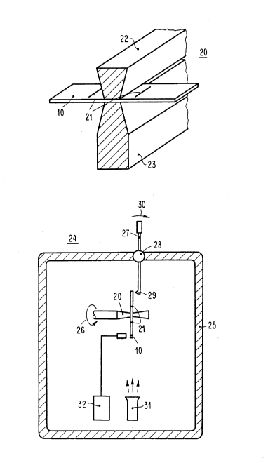
Fig. 2.A is a perspective view of a carrier device for
supporting the laser bar when processed in a
vacuum chamber.
Fig. 2.B is a schematic representation of a vacuum
chamber in which the contamination-free laser
mirror facets are formed and passivated.
Fig. 3 shows laser current degradation curves of
cleaved mirror lasers with (1) a 20 nm Si
passivation, and (2) a conventional A1203
coating.
Fig. 4 shows a light power/operating time (at a power
level of about 300 mW) diagram of a cleaved
mirror laser with a 1 nm Si passivation and an
additional Si3N4 protective coating; it is
compared with diagrams of conventional, Si3N4
-coated devices (operated and destroyed at
lower power levels).
DETAILED DESCRIPTION
Before describing the invention in greater detail,
the purpose and the basic concept underlying the
invention will be briefly outlined by referring to the
experiences and problems encountered with hitherto known
processes and devices.
Important steps in the fabrication process of AlGaAs
(or other III/V compound) laser diodes are the
preparation of the mirrors, conventionally by cleaving,
nowadays also by etching, and their subsequent
passivation. The standard procedure has been to cleave
the laser bar (i.e., the layered structure forming the
~ 2018501
5Z9-89-011 - 8 -
laser waveguide) in air, and to quickly transfer it to a
vacuum system where a protective passivation layer is
deposited onto the mirror facets. The role of this layer
is twofold : (1) it should protect the mirror surfaces
against corrosion, and (2) it should reduce the number of
electrical surface traps resulting from crystal defects.
Both these effects are considered to be responsible for
the energy dissipation during laser operation which
results in mirror degradation and, finally, in excessive
heating of the facets and irreversible catastrophic
damage of the device. Despite the application of
passivation layers, the lifetime of presently known
lasers is still limited by these degradation mechanisms.
Typical light output versus operating time diagrams,
recorded at constant current applied to the laser, show
an initial fast decrease - the so-called "burn-in" phase
- and a normally long phase of smaller degradation rate
with nearly constant slope.
As stated above, the role of the passivation layer
is to prevent any interaction between the surrounding
atmosphere and the AlGaAs while the laser is in
operation. But there exists no such protection against
species that are already present at the mirror surface
when the passivation layer is applied because the mirror
has been exposed to air. Contamination at the AlGaAs -
coating interface is then unavoidable. This is what can
be pre~ented by the present invention.
A first key point of the present invention is,
therefore, to provide a contamination-free mirror facet
and to apply the passivation layer while the laser is
still in the same atmosphere which, of course, must not
lead to surface contamination.
For cleave~ mirror devices, this can be accomplished
by performing the cleaving and the subsequent deposition
of the protective layer "in-situ", e.g., in a vacuum
system with sufficiently low base pressure.
- 2018501
SZ9-89-011 - 9 -
In the case of etched laser devices, the same
principle can be applied. The etched mirror facets are,
when necessary after a cleaning process to obtain a
contamination-free surface, in-situ-coated with the
protective layer.
The applied protective layer can be either the final
passivation layer or a thin layer which has to protect
the AlGaAs surface only until an additional thicker film
is deposited, possibly in a different environment.
The second key point is the choice of a proper
material for the passivation. For different, partly
unknown reasons, the materials used today, mainly SiO2
and A1203, do not result in the desired performance of
the lasers. This aspect required some fundamental
consideration and extensive probing.
The passivation layer must act as a diffusion
barrier for those species capable of reacting with AlGaAs
and, of course, must not react itself with the mirror
material. Since Al, Ga and As do form stable oxides,
oxygen as well as OH or H20 should not be contained in
the material near the laser mirror. So, oxides are
disregarded. Another requirement is that the conductivity
of the passivation layer has to be sufficiently low to
avoid significant currents across the mirror facet. This
eliminates highly conductive materials, such as metals,
unless the layers are made very thin. On the other hand,
the material must form a continuous layer without
pinholes and pores.
In the tests made, best results have been obtained
using Si, but first experiments have shown that Ge and Sb
can also be suitable passivation materials.
Following is a detailed description of an example of
the inventive method where the passivation layer is
deposited on a cleaved mirror facet.
~ 2018501
-
SZ9-89-011 - 10 -
First, a laser bar is produced, i.e., an epitaxially
grown layered structure forming a waveguide which, when
both its ends are terminated with a mirror facet, serves
as the laser cavity. Such bar structure is schematically
shown in Fig.l. It can be the same and fabricated using
the same process as that described in an article by
C.Harder et al, entitied "High-Power Ridge-Waveguide
AlGaAs GRINSCH Laser Diode", published in Electronics
Letters, 25th September 1986, Vol.22, No.20, pp
1081-1082.
Briefly, the sequence of steps for producing the
layered structure 10 is as follows :
The layers are grown on an n + -doped GaAs substrate
11 by, e.g., molecular beam epitaxy (MBE). First, an
n-doped GaAs buffer layer 12 is grown on the substrate.
Next is a lower, n-type cladding layer 13 (0.2 ~m
Alo 45GaO 55As). The core of the laser consists of a
graded n-type region 14 (0.2 ~m Alo 45GaO 55As graded
s Alo.l8GaO 82As), an undoped region 15 forming a
quantum well (7 nm GaAs), and a graded p-type region 16
(0-2 ~m Alo 18GaO 82As graded towards Alo 45GaO 55As)-
Next is the top cladding layer 17 (Alo 45GaO 55As),
followed by a p+ -GaAs contact layer 18 with a doping
density that is high enough for a titanium-platinum-gold
electrode l9A to make good ohmic contact. Another ohmic
contact l9B, at the bottom of the n-type substrate 11, is
obtained by alloying germanium, gold and nickel.
When needed for lateral waveguiding, a ridge, about
5 ~m wide, can be formed on top of the structure (as
shown in Fig.1) prior to applying the metal contact
electrodes. The ridge is obtained by first applying a
photoresist mask to define the ridge. Subsequently, 1 or
2 Aim of the exposed top layers are etched, etching being
stopped 0.2 ~m above the graded-index part of the the top
cladding layer.
2 0 l Y ~ O 1
SZ9-89-011 - 11 -
The further processing of the laser bar 10 will now
be described with the aid of the schematic illustrations
of Fig.2 showing an experimental arrangement. Bar 10,
having a length of several millimeters, is scratched to
provide two scribe lines 21, 750 ~m apart, defining the
position where cleaving and mirror formation is to take
place. It is mounted in a carrier 20 as shown in Fig. 2A.
Bar 10 is held between an upper (22) and a lower (23)
member which apply (through a mechanism not shown) a
gentle pressure to keep the bar in place during
subsequent process steps.
The carrier 20, with the laser bar mounted, is then
placed into a vacuum system 24 as illustrated in Fig.2B.
System 24 comprises an UHV chamber 25 of which only the
outer walls are shown, omitting, for simplicity reasons,
inlets and outlets, electrical connections, etc. In the
chamber, carrier 20 is arranged such that it can be
mechanically manipulated from outside the chamber. For
instance, it can be turned around its horizontal axis as
indicated by arrow 26. The chamber is also equipped with
a lever or "wobble stick" 27, entering the chamber
through a metal bellow 28 allowing for mechanical
movement of the tip 29 within the vacuum chamber. With
the relative position between the lever 27 and bar 10 as
shown, moving the outer arm of the lever to the right, as
indicated by arrow 30, allows tip 29 to apply a force
upon the upper end of the laser bar 10.
In the chamber 25, there is furthermore provided an
e-beam evaporation source 31 for Si deposition as well as
a quartz-crystal oscillator 32 suitable for monitoring
the thickness of the deposited layer during e-beam
evaporation. The vacuum system, the evaporation source
and the crystal oscillator operation are not described in
detail since they are well known in the art. Reference is
made to a "Handbook of Thin Film Technology", edited by
L.I.Maissel and R.Glang (McGraw-Hill, 1970).
~ 2018~01
SZ9-89-011 - 12 -
With the system illustrated in Fig.2B, the sequence
of the required process steps for cleaving and
passivating is as follows :
- After placing the carrier 20 with the laser bar 10
into chamber 25, chamber pressure is reduced to no
more than 1 x 10_6 Pa, preferably about 5 x 10⁻⁸ Pa.
The following process steps can be carried out at
room temperature.
- Moving the end of lever 27 extending outside the
chamber to the right, causes tip 29, located near
the upper end of the laser bar 10, to move to the
left and to break off that end of the bar at the
respective scribe line 21, thereby forming the first
mirror facet.
- After turning carrier 20 by 180 degrees about its
horizontal axis, the same process is repeated,
resulting in breaking off the second laser bar end
at the respective scribe line, thus forming the
second mirror facet.
- Activation of the e-beam evaporation source 31 then
causes the deposition of an amorphous silicon layer
onto the exposed mirror facet facing the source. The
evaporation process is terminated when the thickness
of the layer, monitored by crystal oscillator 32,
reaches the desired value, e.g., 20 nm. By adjusting
the electron acceleration voltage, the evaporation
rate can be set so that the deposition process takes
about one minute.
- After turning carrier 20 again by 180 degrees, the
same evaporation process is repeated, resulting in
the deposition of a silicon layer on the second
mirror facet.
2018501
SZ9-89-011 - 13 -
With this last process step, the passivation coating
is completed and, after packaging, the laser element is
ready for use.
The diagram of Fig.3 illustrates, for a laser
produced with the just described process (curve 35),
i.e., a laser with a 20 nm thick Si passivation layer,
and for a conventional, A1203 -coated laser (curve 36j,
representing the current state of the art, how the laser
power degrades with device operating time.
Curve 35 shows, for the Si-passivated laser, the
output power obtained when applying a constant laser
current (168 mA) over a period of 500 hours at room
temperature. Curve 36, in the same diagram, represents
the corresponding measurement of a virtually identical
laser, except that a conventional A1203 coating had been
applied instead of the Si passivation.
The diagram shows the device behavior during the
first 500 hours of continuous operation. The superior
performance of the Si-coated device, represented by curve
35, is evident : (1) there is virtually no burn-in phase,
i.e., the laser is ready for use immediately after its
fabrication, and (2) the degradation rate has been
determined to be as low as 8.4 x 10⁻⁷ /hour. Testing of
the device has been continued for more than 5000 hours
operating time and has proven that the degradation rate
remained at practically the same low level.
Particularly for high power devices, it proved to be
useful to reduce the Si-film thickness to, e.g., 1 nm, in
which case, however, an additional thick protective
coating is required which may consist of Si3N4.
For such lasers, extremely high light output powers
have been achieved as can be seen from the light-power
versus operating time diagram of Fig.4. Curve 41
represents the performance of a 5 ~m ridge GRINSCH laser
- 2018~01
SZ9-89-011 - 14 -
(as described in the C.Harder et al article cited above)
with a 1 nm Si / 140 nm Si3N4 passivation coating. A 300
mW output beam has been maintained for over 300 hours
without any measurable degradation.
In the same diagram, curves 42 and 43 represent two
laser devices, fabricated on the same wafer and identical
to that of curve 41, except that their passivation did
not contain the in-situ-applied Si. They have been
operated applying laser currents initially resulting in a
light output power of 220 and 180 mW, respectively, but
quickly deteriorated and catastrophic optical damage
occurred after a short operating time.
This comparison illustrates the superior
"power-capabilities" of the in-situ Si-passivated devices
: they allow continuous, long lasting operation at 300 mW
and more, whereas the upper power limit for conventional
devices is far below 150 mW.
First experiences have proven that lasers with
mirrors protected by Ge or Sb layers, instead of Si, also
exhibit a degradation behavior comparable to that of Si
passivated devices if the layers are deposited onto
uncontaminated mirror facets.
The application of the new Si-passivation concept is
not limited to cleaved mirror devices. Any uncontaminated
and stoichiometric mirror face can be protected. An
example are dry etched mirror lasers which are expected
to become increasingly important because they allow full
wafer processing and testing, i.e., passivation coatings
can be applied simultaneously to all devices formed on a
wafer.
A process for fabricating high power etched mirror
lasers with a Si passivation coating in accordance with
the present invention can comprise the following process
steps :
- - 2018501
SZ9-89-011 - 15 -
- Fabrication of the basic layered laser structure (as
described in the C.Harder et al article cited
above);
- Dry etching to produce the etched mirror facets (as
described in European patent application
88.810613.5, filed on September 12, 1988 and
assigned to the present applicant~;
- Sputter cleaning of the etched facets to remove
residuals of the etching process, e.g., with
nitrogen/hydrogen ions, at 800 V and a pressure of
0.4 Pa, followed by annealing to remove surface
defects;
- In-situ e-beam evaporation, i.e., without breaking
vacuum in the system, of a 1 nm Si passivation film,
and
- Sputter deposition of Si3N4 films of different
thickness onto the mirrors at both ends of the laser
waveguide, providing coatings of high and low
reflectivity, respectively.
The invention has been described in detail as
applied to the fabrication of specific AlGaAs ridge diode
lasers with either cleaved or etched mirrors. It should,
however, be understood that it is likewise applicable to
other laser diode structures, and to devices consisting
of compound semiconductors other than AlGaAs. Also,
processes and device parameters may be different from
those indicated herein above. For instance, the Si layers
may be epitaxially grown using a MBE process, then being
crystalline rather than amorphous, and further or
different (other than Si3N4) coatings may be deposited
onto the Si (or Ge, Sb) layer first applied to the mirror
surface.
- 2018501
SZ9-89-011 - 16 -
The key aspects of the invention can be summarized
as follows :
The process of forming a contamination-free mirror
surface, either by cleaving or by cleaning of etched
mirror surfaces, and the subsequent mirror
passivation are executed in-situ in an environment
not causing mirror contamination.
The passivation layer must be continuous, either
insulating or of low conductivity, and of a material
that acts as a diffusion barrier for species capable
of reacting with the mirror surface and that does
not react itself with the mirror material. Suitable
passivation materials are Si, Ge and Sb.
Laser diode devices fabricated in accordance with
the described method are less affected by the
"burn-in" phase, show a significant improvement of
the extrapolated lifetime, and, for a number of
applications most important, allow continuous
operation at drastically increased output power
levels of above 300 mW at room temperature.