Note: Descriptions are shown in the official language in which they were submitted.
'~~~.~~~9
-1- RCA 85,381
METHOD AND APPARATUS FOR CORRECTING TIMING
ERRORS AS FOR A MULTI-PICTURE DISPLAY
This invention relates to apparatus and a method
for reducing the visibility of timing errors in for
example, the inset image of a picture-~in-a-picture
(pix-in-pix) television display system.
In a pix-in-pix system, two images from possibly
unrelated sources are displayed simultaneously as one
image. The compound image includes a full size main image
with an inset compressed auxiliary image. The subjective
quality of the inset image may be affected by timing errors
in either the main signal or the auxiliary signal.
Timing errors relevant to the present invention
may occur, for example, when either the main or auxiliary
signal is a nonstandard signal. As used herein, the term
nonstandard signal means a video signal having a horizontal
line period which rnay vary in length relative to the
horizontal line period set by the signal standard to which
the video signal nominally conforms (e.g. NTSC, PAL or
SECAri~). A noisy but otherwise standard signal may appear
to be a nonstandard signal if the noise is of sufficient
amplitude to mask transitions of the horizontal l~.ne
synchronization (horizontal sync) signal.
To understand how these timing errors may affect
the inset image, it is helpful to know how the auxiliary
signal is processed and displayed. In a conventional
pix-in-pix.display system, the auxiliary signal is sampled
at instants determined by a sampling clock signal which,
desirably, bears a fixed relationship to the horizontal
line scanning frequency of the auxiliary signal. To aid
demodulation of the chrominance signal components of color
television signals, the sampling clock signal desirably has
a frequency that is a multiple of the chrominance
subcarrier frequency. If the multiple is an even number,
e.g., ~, for standard signals, this is a suitable sampling
signal since, under all major video signal standards, it
produces an integer number of samples per line interval.
Under the NTSC system, this sampling clock signal may be
~~~8a~~
-2- RCA 85,381
developed, for example, by a phase locked loop which
produces a sampling signal having a frequency of 4fc, four
times the frequency, fc, of the color subcarrier signal,
and which is locked in phase to color reference burst
component of the auxiliary composite video signal.
The auxiliary video signal is separated into its
component parts, generally a luminance signal and two color
difference signals. These component :signals are then
subsampled both horizontally and vertically to develap
signals that represent a compressed image. The lines of
samples taken during one field of the auxiliary signal are
stored in a memory. These samples are read from the memory
for display using a clock signal that is desirably related
to the horizontal line scanning frequency of the main video
signal.
When the auxiliary signal originates from a noisy
source or from a nonstandard source such as a video tape
recorder (VTR) or a video game, the frequency of the
horizontal sync signal may appear to vary significantly
from line to line while the frequency of the color
subcarrier signal, and thus of the color reference burst
signal, may seem relatively stable. This variation can be
caused by pickup head misalignment or by stretched tape in
a VTR or by inaccuracies in the frequencies used by video
game circuitry. Since, in the example set forth above, the
sampling clock signal is locked in phase to the color
reference burst signal, corresponding samples on successive
lines may be shifted or skewed relative to each other.
When these lines of samples are displayed in synchronism
with the main signal, the pixels produced by these
corresponding samples may not line up vertically.
Consequently, any vertical lines in the inset image may
appear jagged (if the period of the horizontal sync signal
changes randomly) or tilted (if there is a fixed error in
the relative frequencies of the horizontal sync and color
burst signals). The frequency and phase variations which
cause this type of image distortion are known as timing
errors or, alternatively, as skew errors.
-3- ~2CA 85,381
One type of timing error, which is relevant to
the present invention, results from frequency or phase
variations between the main horizontal sync signal and a
video display clock signal that is phase locked to the
color reference burst component of the main signal. Errors
of this type may randomly change the distance between the
left side edge of the main image (defined by the horizontal
sync pulses) and the beginning of lines of 'the inset image
(defined by the display clock signal). Main signal timing
errors of integral numbers of sampling clock periods may be
compensated for in the phase locked loop circuitry which
generates the horizontal sync signal. Skew errors which
are a fraction of a sampling cloak period may be more
difficult to correct.
One method of correcting these 'types of timing
errors is to use interpolation to develop sample values
that axe matched to the clock signal used to store or
display them. Another method is to shift the phase of the
clock signal used to display the sample values so that it
is properly aligned to the horizontal sync signal. These
methods are described in U.S. Patent No. 4,638,360 entitled
'tTiming Correction for a Picture-In-Picture Television
System".
Skew errors may also be corrected by generating
samples that represent component video signals in
synchronism with a skew shifted line locked clock sa.gnal.
These samples are then applied to clock transfer circuitry
which aligns the samples with a line-locked clock signal
that is not skew shifted. U.S. Patent No. 4,782,391
entitled "Multiple Input Digital Video Features Processor
for TV Signals, " relates to a system of this type.
The first two methods described above use two
substantially independent clock signals. Aside from the
extra circuitry used to generate an additional clock
signal, systems which use multiple clock signals may need
to be carefully shielded to prevent radio-frequency
interference between the signals.
-~° RCA 85,381
In the third method described above, the
luminance and color difference signal components of the
auxiliary signal are separated by analog circuitry and 'then
digitized. A system using this method may be more complex
than a system which digitizes the composite video signal
and then separates it into its component parts. In
addition this second method uses line-locked clock signals,
so it may be difficult to encode the color information
signals of the compressed video signal so that the two
signals may be time-division multiplexed for display.
The present invention is embodied in a system
which compensates for timing errors in a first video signal
relative to a second stored video signal. This system
includes a first clock signal .far retrieving samples of the
second stored video signal from memory. A signal phase
alignment circuit shifts the phase of the first clock
signal to generate a second clock signal that is
synchronized to the horizontal scanning signal derived from
the first video signal. A clock transfer circuit,
responsive to the second clock signal, aligns retrieved
samplessynchronous with the first clock signal, to a
predetermined phase relationship with the phase shifted
clock signal.
Brief Descrii~tion of the Drawings
FIGURE 1 is a block diagram of a television
receiver which includes an embodiment of the present
invention..
FIGURE la is a block diagram of exemplary
circuitry for generating a subsampling clock signal used in
the television receiver shown in FIGURE 1.
FIGURE 2 is a block diagram of a clock phase
shifter suitable for use in the television receiver shown
in FIGURE 1.
FIGURE 3 is a block diagram of circuitry which
illustrates the operation of the signal phase alignment
circuitry shown in FIGURE 2.
-5- RCA 85,381
FIGURE 4 is a block diagram of clock transfer
circuitry suitable for use in the television receiver shown
in FIGURE 1.
FIGURE 5 is a timing diagram which is useful for
describing the operation of the clock phase shifter
circuitry shown in FIGURE 2.
The present invention is de.acribed in the context
of digital circuitry which implements, for example, a
pix-in-pix feature for a consumer television receiver. It
is contemplated, however, that this invention has broader
application. It may be used in other systems where two
images or portions of two images are displayed concurrently
(e.g., side by side or one over the other) and it may
employ analog circuitry, such as charge-coupled devices, in
place of the digital memory circuitry.
In the television system described below, a main
video signal is processed by conventional analog circuitry
to produce a full-size image. An auxiliary signal is
received, digitized and processed by digital circuitry to
produce a luminance signal and two quadrature phase related
color difference signals. These separated signals are
subsampled to develop signals representing a compressed
image. The subsampled signals are stored in a memory which
holds one field interval of the compressed signal. When
the compressed image is to be displayed, the stored signals
are retrieved from the memory and encoded into a composite
video signal. This composite video signal is substituted
for a portion of the main composite video signal to
generate a compound signal which is processed by the analog
circuitry to display a compound image. This compound image
includes a full-size main image with a compressed auxiliary
image displayed as an inset.
A composite videa signal includes three component
signals, a luminance signal, Y, and two color difference
signals, for example, (R-Y) and (~-Y). The two color
difference signals modulate respective c~.xadrature phase
~~~~~29
-6- RCA 85,381
related color subcarrier signals to produce a chrominance
signal which is additively combined with the baseband
luminance signal to generate the composite video signal.
Conventional analog techniques for decoding a composite
video signal include low-pass filtering to recover the
luminance signal, Y, and band-pass filtering to recover the
chrominance band signals. The chrominance band signals are
then synchronously demodulated using a regenerated color
subcarrier signal.
zn general, when digital processing techniques
axe used, a composite video signal is first sampled and
digitised. The sampling clock signal used to develop these
samples is typically lacked in phase to the color burst
signal of the composite video signal. This sampling signal
may aid in the demodulation of the Chrominance signal. E'or
example, if the selected sampling clock signal has a
frequency of 4fc, four times the frequency, fc, of the
color subcarrier signal, successive samples of the
separated chraminance signal may be represented by the
SeqllenCe (R-Y), (B-Y), -(R-Y), -(B-Y), (R-Y)r etC. where
the minus signs indicate sampling phase and not necessarily
sample polarity. The (R-Y) and (B-Y) color difference
signals may be recovered from this sequence by a process of
demultiplexing and selective polarity inversion.
Thus, if these conventional techniques are used
to decode the chrominance signal components of two
independent Composite video signals, it is desirable to
generate two oscillatory signals related to the respective
Color subcarrier signals of the two composite video
signals. Using two clock signals may complicate the design
of the receiver, since electromagnetic shielding may be
needed, to limit interference between the two signals.
An alternative method far demodulating two video
signals is to generate only one oscillatory signal, for
example, the main signal color subcarrier signal. This
signal is then used to generate a sampling Clock signal for
digital Circuitry which processes the auxiliary signal.
However, since the Chrominance signal phases of the main
-7- ~tCA 85, 381
and auxiliary signals may be different, it may be desirable
to include circuitry which corrects the phase of the
digitized decoded Color difference samples based on the
color reference burst component of the auxiliary signal.
The choice of a sampling clock signal is also a
factor in determining what type of skew-error compensation
circuitry is to be used in the system. Since a clock
signal that is locked to the main burst signal may be less
closely aligned to the auxiliary horizontal sync signal
than a clock signal that is locked to the auxiliary burst,
the possibility of skew errors when the compressed
auxiliary signal is stored in the memory is increased.
Moreover, if the sampling clock signal is locked to the
main signal burst, skew errors caused by noise in the main
Z5 signal or by variations in the relative frequencies of the
main signal horizontal sync and color subcarrier signals
are not reduced. A sampling clock signal that is locked to
the horizontal synchronizing component of the auxiliary
signal may also be used.
Tn the television receiver described below, skew
errors of the first type are reduced to a maximum of
one-third of one clock period (e.g. to a maximum of 23 ns
for a sampled data NTSC signal having a sampling frequency
of ~fc) and skew errors of the second type are
substawtially eliminated.
In the system described below, the luminance
signal component of each horizowtal line interval of the
auxiliary video signal is subsampled in a six to one ratio
and then displayed at a sample rate that is one-half of the
4fc sannpling clock signal derived from the main signal
burst. This results in an effective sampling ratio of
three to one. Thus, the effective subsampling clock signal
has a frequency that is one-third of the frequency of the
clock signal used to display the samples. When the
subsampling clock signal is generated, signals having six
different evenly spaced phases are provided. Skew errors
of the first type are reduced by selecting the best one of
these six possible subsampling clock signal phases at the
°
8- RBA 85,381
start of each horizontal line of the auxiliary video
signal. The selected phase is determined by the relative
timing of each phase to the auxiliary horizontal sync
signal.
Skew errors of the second type are substantially
eliminated by using phase alignment circuitry to generate,
from the main clock signal, a display clock signal that is
aligned to signals which control the horizontal scanning of
the display. A clock transfer circuit is then used to
translate samples that are provided in synchronism with the
main clock signals into samples that are synchronous with
the display clock signal. Since The display clock signal
is derived from the main clock signals, there is no
distortion of the output samples caused by frequency
differences between the two clock signals.
In the drawings, broad arrows represent signal
paths for conveying multi-bit digital signals. Line arrows
represent connections for conveying analog signals or
single-bit digital signals., Depending on the processing
speed of the devices, compensating delays may be required
in certain of the signal paths. One skilled in the art of
digital signal processing circuit design will know where
such delays are needed in a particular system.
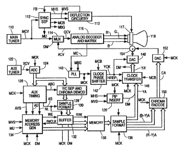
FIGURE 1 is a block diagram of a television
receiver having a pix-in-pix feature which includes an
embodiment of the present invention. In FIGURE 1, a main
composite video signal, MCV, provided by a main tuner 110
is applied to conventional synchronization signal
separation circuitry 112. The circuitry 112 generates
signals MEiS and Mt7S representing, respectively, the
horizontal line and vertical field synchronizing signal
components of the signal MCV. The circuitry 112 also
provides a main burst-gate signal, NtEG, a signal i~ItT which
indicates when the signal MCV is the upper field of an
image and a main composite blanking signal, Id3C8. The
signal MCP as generated by phase locked loop circuitry
which uses a horizontal fly-back signal, FE, generated by
-9- FICA 85, 381
deflection circuitry 113, as a reference signal.
Consequently, the signal MCB is locked to the horizontal
line scanning signals used to produce 'the video display.
Tt is relatively independent of noise in the signal MCV and
tends to track variations in the scanning frequency .related
to the loading of the high-voltage supply.
The signal MCV is also appliaed to one input
terminal of a multiplexes 114. Another input terminal of
the multiplexes 114 is coupled to receive a composite video
signal ACV representing a compressed auxiliary image. The
multiplexes 114 is controlled by a signal, DM', to
substitute the signal ACV for the signal MCV in a portion
of each field. The signal DM' is generated by pix-in-pix
insertion circuitry 120 and clock transfer circuitry 146 as
described below. The compressed signal, ACV, is
substituted for the main signal, MCV, when the signal DM'
is logic-zero. The output signal of the multiplexes 114 is
a compound composite video signal, CCV, representing the
main image with an inset auxiliary image.
The pix-in-pix insertion circuitry 120 is
responsive to the main horizontal and vertical
synchronizing signals, MVS and MISS, and to a clock signal
MCK to generate the signal DM. The signal DM is applied,
as set forth below, to the clock transfer circuitry 146 to
produce the signal DM' which is aligned to the horizontal
scanning signal used to produce the compound display. In
the present embodiment of the invention, the compressed
auxiliary image is displayed during 69 successive line
inteZwals during each field of the main signal. Each
displayed compressed line occupies approximately
one-quarter of the corresponding main signal horizontal
line interval.
The output terminal of the multiplexes 114 is
coupled to conventional analog decoder and matrix circuitry
7.16 which, for example, separates the luminance and
chrominance signal components of the signal CCV,
demodulates the chrominance signal component into
quadrature phase related color difference signal components
~~~~ i~9
-10- RCA 85,381
and generates, from the luminance and color difference
signals, red (R), green (G) and blue (B) primary color
signals for application to a cathode-ray tube (CRT) 118.
The image represented by the signal CCV is reproduced on
the CRT 118 under control of deflection signals generated
by -the~deflection circuitry 113.
An auxiliary composite video signal, XCV, from
which the signal ACV is generated, is provided by a
conventional television tuner 122. The signal XCV is
ZO applied to an analog-to-digital conve:cter 124 which is
clocked by the sampling clock signal I~tCK. The signal MCK
is generated by phase locked loop (PLL) circuitry 140. The
circuitry 140, which may include a conventional
burst-locked PLL is responsive to the main chrominance
signal component, NiC, provided, for example, by the analog
decoder and matrix circuitry 116, and to the main
burst-gate signal, EKBG, to generate the clock signal MCK
which has a frequency, 4fc, four times the frequency, fc,
of the color subcarrier signal component of the signal MCV.
The signal l~iCK is locked in phase to the color
synchronizing burst signal component of the main signal
IYlCV .
The color burst signal is a reference signal
having a predetermined phase relationship with the color
subcarrier signal component of a composite video signal.
Thus, the ADC 124 produces samples of the auxiliary signal,
XCV, that are synchronized to the chrominance subcarrier
signal component of the main signal, MCV.
The samples provided by the ADC 124 are applied
to auxiliary timing circuitry 126 which, responsive to the
signal MCK, generates sa.gnals AVS, ABG, Atl, AS and NL. The
signal AVS is the vertical field synchronizing signal for
the auxiliary video signal. The signal ABG is the
auxiliary burst-gate signal. The signal AU indicates when
the auxiliary samples are from an upper field or from a
lower field. The signals AS and NL are pulse signals that .
indicate which gixels and lines, respectively, of the
auxiliary signal may be used to form the compressed image.
-11- ~~~~~~~ RCA 85,381
These signals eliminate several lines on the top and bottom
of the image and several pixel positions on the left and
right sides of the image. These portions of the image are
eliminated to reduce the amount of memory used to store the
image and to reduce the size of the inset in which the
auxiliary image is displayed.
As set forth above, the subssampling signal AS is
adjusted in phase at the start of each horizontal line
period of the auxiliary signal. This phase adjustment
effectively selects one of six phase shifted subsampling
signals generated from the signal MCK. Using this
adjustment, skew errors in the display caused by
differences in the relative 'times of occurrence of the
auxiliary horizontal sync pulse and the first stored pixel
are limited to 23 ns [1/(l2fc)]
FIGURE la shows exemplary circuitry for
generating the subsampling signal AS. This circuitry is a
part of the auxiliary timing circuitry 126. In FIGURE la,
the signal MCK is applied to a frequency divider 160 which
is xeset by the auxiliary horizontal sync signal, AHS. The
output signal of the frequency divider 160, which has a
frequency of 2fc/3, is applied to a seven-bit counter 162
which is reset by the signal AHS. The output signal of the
counter 162 is coupled to first and second decoders 164 and
166. The decoders 164 and 166 produce logic-one output
pulses when the value provided by the counter 162 is equal
to 19 and 127, respectively. The values provided by the
decoders 164 and 166 are used to set respective RS
flip-flops 168 and 170. These flip-flops are reset by the
signal AHS. The output signal of the flip-flop 168 and the
inverted output signal of the flip-flog 170 enable an AND
gate 1?4 to pass the signal provided by the frequency
divider 160 during the central portion of each auxiliary
line. Since the frequency divider 160 is reset at the
start of each horizontal line period, the phase of the
subsampling clock signal AS may vary from line to line to
track the phase of the signal AFIS.
-12- RCA 85,381
The samples generated by the ADC 124 are applied
to a luminance-chrominance (Y/C) separator and chrominance
signal demodulator 128, which is also coupled to receive
the signal ABG provided by the auxiliary timing circuitry
126. The Y/C separator portion of the circuitry 128 uses a
standard low-pass and band-pass filter arrangement to
separate luminance signal and chromina.nce-band signals from
the auxiliary composite video signal. The chrominance
signal demodulator portion of this circuitry separates the
chrominance band signal into two quadrature phase related
color difference signals. for example, (R-Y) and (~-Y).
Since the signal XCV is sampled synchronous with
the color subcarrier signal of the main signal, the color
difference samples provided by the circuitry 128 may need
to be shifted in phase to correct for phase differences
between the color subcarrier signals of the main and
auxiliary video signals. To this end, the circuitry 128 is
coupled to receive the auxiliary burst-gate signal, AEG,
provided by the timing circuitry 126. Responsive to this
signal, the circuitry 128 monitors the color burst signal
component of the sampled data auxiliary signal and corrects
the phase of the demodulated color difference signals on a
line-by-line basis. Exemplary circuitry for performing
this function is described in U.S. Patent ~to. 4,558,348.
The output signal from the Y/C separator and
ehrominanee demodulator 128 is applied to a sample
formatter 130. The formatter 130 is responsive to the
signal AS.to horizontally subsample the sampled data
luminance signal in a six to one ratio and to subsample
each of the sampled data color difference signals to
produce respective compressed color difference signals
having a sampling frequency of fc/9 (4fc/36). This
horizontal subsampling compresses the auxiliary image in a
three-to-one ratio when the luminance signal is displayed
at a sample rate of 2fc and the color difference signals
are displayed at an effective sampling rate of fe/3.
Using this subsampling scheme. one pair of
samples, representing the two color difference signals, is
-13- ~~ ~~~ RCA 85,381
produced for each six luminance samples. The formatter 130
reduces each of the luminance and color difference samples
to six bits of significance and combines the luminance and
color difference samples such that six bits of each
eight-bit output sample represent luminance information and
the remaining two bits represent one bit each of two
corresponding color difference signal samples. This
technique spreads each pair of color difference samples
across six consecutive luminance samples. The sample
formatter 130 provides these eight-bit samples to a buffer
132.
Samples provided to the buffer 132 are stored in
a first-in-first-out (FIFO) memory (not shown) which is
internal to the buffer 132. The stored samples are
transferred from the buffer 132 to a memory 136 under
control of memory address generation circuitry 134. The
circuitry~134 also controls the reading of samples from the
memory 136 for display. In writing samples into the memory
136, the circuitry 134 vertically subsamples the
horizontally subsampled auxiliary signal to generate
samples representing a vertically and horizontally
compressed image. The memory 136 used in this embodiment
of the invention includes a sufficient number of storage
cells to hold one field of samples of the compressed image.
Samples are read from the memory 136 at a 2fc
rate responsive to the address signals provided by the
memory address generator 134. These samples are processed
by the cirEUitry described below to generate the composite
video signal ACV which is combined with the signal MCV, as
set forth above, to generate the compound pix-in-pix image.
The samples read from the memory 136 are applied
to a sample formatter 138. The Formatter 138 reverses the
process performed by the formatter 130, to provide a
separate luminance signal and two separate color difference
signals, each occurring at a 4fc sample rate. However, in
this embodimewt of the invention, the luminance samples
change value at a maximum rate of 2fc and the color
difference samples change at a rate of fc/3. The sampled
-14- ~~~~~~~RCA ~5,s81
data (R-Y) and (B-Y) color difference signals are applied
to a chrominance signal encoder 150 which interleaves,
interpolates and selectively inverts the color difference
samples to generate a sampled data chrominance signal. The
effective color subcarrier signal of this sampled data
chrominance signal has the same frequency and phase as the
color subcarrier of the signal MCV sine:e the clock signal,
MCK, used by the encoder 150 is burst-:Locked to 'the main
signal.
The sampled data luminance signal, YA, provided
by the formatter 138 and the signal DM provided by the
pix-in-pix insertion circuitry 120 are applied to the clock
transfer circuitry 146. The circuitry 146, described below
in reference to FIGURE 4, changes the timing of its input
signals to generate signals YA° and DM' which are
synchronous with the clock signal YCK. ,
The signal YCK is phase aligned to horizontal
synchronizing signal components of the main composite
signal. Clock phase shifting circuitry 142, described
below in reference to FIGURES 2 and 3, generates the clock
signal YCK by providing multiple phases of the signal MCK
and the selecting one of these phases as the signal YCK.
The selected phase is the one most closely aligned to a
horizontal line scanning reference signal derived from the
signal MCB.
The signal CA, provided by the chrominance signal
encoder 150, is not aligned to the signal YCK. This
preserves.the alignment of the chrominance signals of the
compressed and main video signals. While the lack of
alignment may cause skew errors in the color signals used
in the compressed image, these errors are not noticeable
since the human eye is less sensitive to changes in color
than to changes in luminance and since the minimum rise
time of a chrominance signal is much longer than for a
luminance signal.
The signals YA' and CA are applied 'to respective
digital-to-analog converters 148 and 152 which generate
analog signals corresponding to the respective sampled data
~~~.8~2~
-15- RCA e5,3s1
digital signals. These analog signals are combined in
summing circuitry 154 to generate the analog composite
video signal ACV which is substituted for.a portion of the
main signal MCV to generate the compound composite video
signal, CCV.
Instead of multiplexing the signals MCV and ACV
to develop signals representing the compound image, it is
contemplated that circuitry may be inserted in the analog
decoder 116 to multiplex the signals Y,A.' and CR with
respective separated main luminance and chrominance
signals. Moreover, it is contemplated that other component
signals such as YA° and (R-Y)A and (B-Y)A or auxiliary R,
G, and B primary color signals may be multiplexed with
corresponding signals derived from the main video signal to
generate signals representing the compound image.
FIGURE 2 is a block diagram of circuitry suitable
for use as the clock phase shifter 142. In FIGURE 2, the
main clock signal MCK is applied to a set of 13
cascade-connected buffer gates 212. In this embodiment of
the invention, each of the gates 212 is realized as a pair
of logical inverters. Each of the buffer gates 212 delays
the signal applied to its input port by a fixed amount of
time. Thus, the output signals provided by the inverters
212 represent respectively different phases of the signal
MCK. Ideally, the total delay through all of the serially
connected buffer gates 212 is substantially equal to one
period of the signal MCK. However, due to process
variations~in the manufacture of integrated circuits
containing the clock phase shifter 142, variations in the
so total delay may ~rary by as much as -50~ to øloo~.
The signals representing 14 different phases of
the signal MCK, provided by the buffers 212, are applied to
signal phase alignment circuitry 210. The circuitry 210
selects one of these signals as being the most closely
aligned in phase to the horizontal scanning component of '
the main composite blanking signal MCB. The signal MCB is
applied as a reference signal 'to the circuitry 210.
~~~~ ;~.~2,
-16- RCA 85,381
FIGURE 3 is a block diagram of simplified phase
alignment circuitry which illustrates the operation of the
circuitry 210. This circuitry includes only four stages
instead of the 14 stages of the circuitry 210. To add
additional stages to this signal phase alignment circuitry,
the elements delimited by the broken lines 335 are
replicated as many times as desired. The circuitry shown
in FIGURE 3 is similar to circuitry described in U.S.
Patent 4,824,879 entitled, '°Signal Phase Alignment
Circuitry, " . The
present circuitry differs from the referenced circuitry
only in the addition of a pseudo-stage 355 which includes
A~dD gates 354 and 358, an inverter 356 and an OR gate 357.
The circuitry shown in FIGURE 3 operates as
follows. Responsive to a positive-going transition of the
signal MCB, instantaneous samples of each of the different
phases of the signal MCK are stored in respective n-type
flip-flops 310, 320, 330 and 340. Since the total delay
provided by the buffer gates 212 approximates one period of
the clock signal MCK, the values stored in these flip-flops
represent a '°snapshot°' of all of the phases of the signal
MCK at the different taps, taken at the transition of the '
signal MCB.
If this "snapshot" includes a positive-going
transition of the signal MCK (which appears as a
negative-going transition of the samples from the delay
line when read from left to right), one of the flip-flops,
for example, 320 will have a logic-one output signal and
the next successive flip-flop, 330 will have a logic-zero
output signal. In this instance, all of the input signals
to an At3D gate 334 will be logic-one. In this instance,
the output signal of the A1~1D gate 334 will enable the clack
phase signal provided by a buffer gate 212b to pass through
an AtdD gate 338 and an OR gate 360 as the output signal of
the phase alignment circuitry.
i~hen the "snapshot" stored in the flip-flops 310,
320, 330 and 340 includes more than one transition,
inhibiting circuitry which includes inverters 316, 336, 346
-1?- RCA 85,381
and 356 as well as OR gates 337, 347 and 357 allows only
the clock signal phase corresponding to the first
transition to be selected as the signal YCK. When the
"snapshot" includes only a negative-going 'transition, or
when the sample values held in the flip-flops are all
logic-one, indicating no captured transition, the clock
signal phase provided by the buffer gate 212c is selected
as the ghase aligned output signal YCK. This selection is
accomplished by the pseudo-stage 355. Finally, when the
"snapshot°' does not include any transi~tians but the values
held in the various flip-flops are all logic-zero, the
signal MCK is selected as the phase aligned output signal,
YCK, by the action of AND gates 314 and 318 and an inverter
316.
Referring to FIGURE 2, the signal YCK is applied
to the clock input terminals of three serially connected
delay elements 216, 218 and 220. The data input signal to
the first of these delay stages, 216, is the signal MCB as
delayed by six buffer gates 214. The buffer gates 214
delay the signal MCB by an amount of time equal to the
propagation delay through the signal phase alignment
circuitry 210 plus an amount of time needed for the output
signal of the circuitry 210 to become stable. This
stabilizing time may be equal, for example, to the maximum
signal propagation delay through the inhibiting circuitry.
The six buffer gates 214 shown in FIGURE 2 are exemplary.
The exact number used depends on the number of stages in
the alignment circuitry 210 as well as the technolocly in
which it is implemented.
The delay elemewts 216, 218 and 220 each delay
the signals applied to their respective input ports by one
period of the signal YCK. The output signal of the delay
element 218 and an inverted version of the output signal of
the delay element 220 are applied to respective input
terminals of an AND gate 224. The AND gate 224 provides an
output signal HREF which is syxzchronized to the signal YCK
but is delayed with respect to the signal MCB by an amount
of time that is fixed to within the resolwtion of the
-18-- ~~~~~~~ I2CA 85,381
signal phase alignment circuitry 210. That is to say,
transitions of the signal Ht~EF occur with a substantially
fixed delay with respect to corresponding transitions of
the signal MCB. The maximum error in this delay is the
signal propagation delay time through one of the buffer
gates 212.
As shown in FIGURE 1, the signals YCK and I3REF
are applied to clock transfer circuitry 146 to align the
signal DM and the samples of the signal YA to the
horizontal line scanning signals that are used to display
the compound signal. FIGURE 4 is a block diagram of
exemplary clack transfer circuitry 146. In overview, the
circuitry shown in FIGURE 4 operates as follows. Samples
of the signal YA are transferred from a register 47.0 into
registers 418, 416, 414, and 412 on a rotating basis
synchronous with the main clock signal, MCK. Sample values
are read~from the registers 418, 416, 414 and 47.2, also on
a rotating basis, synchronous with the signal YCK. These
sample values constitute the signals DM' and YA°.
The following is a more detailed description of
the circuitry shown in FIGURE 4. The signal MCB is applied
to an edge detector 425 which includes clocked delay
elements 424 and 426, an inverter 428 and an AND gate 430.
The output signal of the edge detector 425 is a pulse
signal, Wit, that is synchronized with a positive-going
transition of the signal MCB. The signal HI~t is applied to
the reset input terminal of a modulo-four counter 432. The
clock input terminal of the counter 432 is coupled to
receive the main clock signal, MCK. The output signal of
the counter 432 is applied to a decoder 434. The decoder
434 produces a logic-one output signal when the value
provided by the counter 432 is zero and a logic-zero output
signal otherwise.
The output signal of the decoder 434 is a pulse
which occurs once every four periods of the signal MCK and
has a pulse width substantially equal to one period of the
signal MCK. This signal is applied to three ser~.ally
connected delay elements 436, 438 and 440. Each of these
-19~ " """"°A'CA 85,381
delay elements delays the signals applied to its input port
by one period of its clock signal MCK. The output signals
of the decoder 434 and the delay elements 436, 438, and 440
are applied to respective load input terminals of the
registers 418, 416, 414, and 412.
Responsive to the pulse signal provided by the
decoder 434, the register 418 is conditioned to load a
sample value of the combined signals YA and DM from the
register 410. During the next period of the signal MCK,
the pulse signal propagates to the output terminal of the
delay element 436. Responsive to this signal, the register
416 is conditioned to load the next subsequent sample of
the signals YA and DM from the register 410. In the same
way, the registers 414 and 412 are conditioned to load the
next two respective samples of the combined signal YA and
DM.
Sample values are read from the registers 412,
414, 416 and 418 under control of a modulo four counter
422. The counter 422 is reset by the signal HREF' and
clocked by the signal YCK. The output values provided by
the counter 422 are applied to a multiplexer 420 to
sequentially gate the values held in the registers 418,
416, 414 and 412 to the input port of a register 442. The
register 442 is responsive to the signal YCK to load a new
value. The output signal provided by the register 442 is
the aligned and compressed luminance signal, YAp. Although
this signal is provided for each horizontal line interval -
in each field of the main video signal, it is only valid
during the portion of the 69 line intervals in which the
compressed image is displayed.
FIGURE 5 is a timing diagram which illustrates
the operation of the clock phase shiftier 142 and the clock
transfer circuitry 146. The signals MCK and MCB are
applied to the clock phase shifter 142. The skew error
between the exemplary signals MCK and MCB is illustrated as
the time interval T1. In this embodiment of the invewtion,
the time interval T1 may have values ranging from 0 ns to
70 ns.
-20- ~~~~~~~RCA 85,381
Responsive to the signals MCK and MCB, the clock
phase shifter 142 generates the clock signal YCK that is
aligned to the signal MCB and thus to 'the horizontal line
scanning signals used to display the compound image on the
CRT 118. The negative-going transition 510 of the signal
YCK is in a substantially fixed time relationship with the
positive going transition of the signal MCB. The time
interval between these two transitions may vary, from line
to line, by the propagation delay through one of the buffer
gates 212. The transition 508 of the signal YCK is
nominally aligned with the positive-going transition of the
signal MCB, but, due to propagation delays through the
gating circuitry of the phase alignment circuitry 142 and
through the inhibiting circuitry of the signal phase
alignment circuitry 210, the transition 508 may not occur
in the same time relationship with the signal MCB from line
to line.
The buffer gates 214 are included in the phase
shifter 142 to compensate for this instability in the
transition 508. These gates prevent the signal MCB from
propagating to the delay element 216 until the clack signal
YCK has stabilized. The signal HREF, which is generated by
the clock phase shifter 142 from the delayed signal MCB,
and the clock signal YCK also have substantially fixed
timing relationships with the signal MCB. The time
interval T2 between the positive going transitions of the
signals MCB and HREF varies by. at most, the propagation
delay through one of the buffer gates 232. In this
embodiment of the invention, that propagation delay is
approximately 5 ns.
The signals i~tCK, MCB, YCK, HREF and YA are
applied to the clock transfer circuitry 146, The output
signal of the circuitry 146 is the phase aligned luminance
signal YA' and the phase aligned control signal for the
multiplexer 114, DM'. The signal HI~i is generated internal
to the clock transfer circuitry 146. This signal begins
the storage of sample values of the signal YA into the
registers 412. 414, 416 and 418. The signal I1REF begins
-21- ~~~~~~~RCA 85,381
the retrieval of sample values from these registers. As
shown in FIGURE 5. the signal HREF is delayed by more than
one period of the signal MCK relative to the signal AIM.
This delay ensures that the sample values stored in the
registers 412, 414, 416 and 418 are v<~lid when 'they are
read under control of the counter 422.. In this embodiment
of the invention this one clock period delay between the
signals HI2EF and R'M is provided by the delay element 436 of
the clock transfer circuitry shown in FIGURE 4.
to since the signals HREF and YCK are aligned with
the horizontal scanning signals used to produce the
compound display, vertical lines in the inset image,
including the image borders, are displayed with
significantly less skew error than if the signals HM and
MCK were used. The skew errors related to the sampling of
the auxiliary signal sgnchronous with the signal MCK are
apparent only on vertical or near-vertical lines in the
image. These errors are generally less noticeable than
skew errors in the border of the compressed image which are
caused, primarily, by instantaneous phase differences
between the system clock signal and the horizontal scanning
signals.
while the invention has been described in terms
of an exemplary embodiment, it is contemplated that it may
be practiced as outlined above with modifications within
the spirit and scope of the appended claims. For example
if the invention is practiced in the environment of a video
cassette recorder (VCR), blanking signals are nominally
unavailable. In this instance signals derived from the
vertical and horizontal synchronizing signals MHS and MVS
will be utilized instead of the signal MCP. It is also
contemplated that auxiliary input signal may be in
componewt form obviating thv circuitry 128. Further, a
system may be arranged to combine main and auxiliary
baseband luminance and chrominance components at
multiplexer 114 in which case the main clock signal may be
derived from a source other than the main video color
reference burst signal, i.e., from the color reference
-22-~ ~~~~~~~ RcA s5,3s1
signal of the auxiliary signal or the auxiliary horizontal
synchronizing signal, etc. In a system for displaying two
images side-by-side, the subsampling and interpolation
elements of the exemplary system may be eliminated, and/or
the sample formatting elements may be eliminated with the
component signals stored in separate portions of the
memory.
It should also be appreciated that in an
arrangement where the auxiliary image is not compressed for
display, but possibly only cropped, as for a sidembymside
display, the auxiliary signal may be sampled and stored in
memory in composite form. After the signal is retrieved
from memory it may thereafter be separated into component
form for realignment of the luminance component and
synchronization of the auxiliary chrominance subcarrier
with the main video chrominance subcarrier.