Note: Descriptions are shown in the official language in which they were submitted.
. 20~8~3~ ~
~, ~.` . ` .
. C . POWER. CON'rROLLER WITH SEIORT CIRCUIT }\_V OVEJ~LOl\D PROTEC'I'IOI`l
sackgl-ound of The Invention
The present invention rel~tes to power control circuits
and more particularly relates to circui~ bre~kers providinq o~tel~
load and short circuit protection.
Presently available circuit breclkers oE the electr.o~
magnetic or thermal type are known to llave turn o~f times in the
range of 10 milliseconds or more. This l0 millisecond turn off
time is dangerously too long in-many critical circuit breaker . .
applications, such as military, flammable or explosive environmen~
~urthermore, in large electrical systems, the tripped c~rcuit
breaker must be located and subsequently re-set manually in order
to.restore the circuit after the fault has been cleared. These
probl~.ms of long turn off times and manual resetting associated
with mechanical circuit breakers may be disadvantageous and very
serious in applications where time is a critical factor.
The Triac is a conventional e.l.ectronic power device ~: .
made of silicon crystal comprising a dual sense silicon control leJ - :
recti~ier (SC~) for receivillg a gate signal for controlling power ~;
through a load, such as in large wattage dimmer devices. One
problem assoclated ~ith SCR or Triac devices in power control. ;~
applications is that once the Triac is turned on, it will not :
turn of unless the supply voltage or current is cut off, or
else turn off will not occur until the next zero crossing of the
A.C. power supply. This time duration required to turn off the
Triac may be as much as one half of the ~.C. cycle, resulting in
damaging the Triac under overload and short circuit conditions. ~:
In the United States Patent No. 4,h33,161 issued to
20~L8~31
. Callahan et al on ~ecember 30, 1986, there is descl-ibed an
3 inductorless phase control c1i~ner power contl-ol~er for couplinq
a l~np to an ~lternating current source. This patent is dlrecl:e~
to the elimination of the filter inductor from the power stage of
the conventional solid state electronic dim~er. i~ere, in thi.s
dimmer controller, the main power is dissip~t:ed in ~he diodes
of a pair of power MosFErr due to the forward voltage drop across
the FET diod~s which are used as the current con~ucting path for
the dimmer load. This results in excessively high power
~ dissipation in the FET devices due to hi~h vc~ltage/l1igh current
I operation in the linear mode. Thus, such i~ductorless dimmer --
power controller may be used in lower power dimmer applications,
but would dissipate too much heat and burn o~it if employed in
the higher power control circuits. This burn out occurs
since the internal clamp diode, being located in tl1e same case
as the MOSFET, increases in temperature, and consequently
i increases the MOSFET's RDS/on, thereby increasinq the
I dis~ipation on the MOSFET itself. Also, the power dissipation ~-
in the patented power control device is increased across the
MoSFET since the l~ad current rise time is increased for the
purpose o eliminating the EMI filter inductor by orcing it ;
1 to operate in the linear mode. Thus, by turning the FETS on
slowly, as occurs when turning on the MOSFET as half cycle in
the linear mode, large heat dissipation in the MOSFET will
result. Furthermore, the absence of thé inductor wi.ll allow
fast current rises in the case of a short circui~ OL^ overload
I condition, faster than the response of the current limit circuiti The only ele~tent that controls the current slew rate is the li.ne
inductance. ~f the fault occurs At lJ4 cycle, where the line~
voltage equals the plus or minus peak value, and the electric
line to the load is short, the efficiency of the current limit
circuit is questionable in view of the maxim~ allowed load
current in the linear mode. This also contributes to the
high heat dissipation in the MOSFET power aontrol ~vice.
2~8~3~
lIn view of the above, it is an ob~ect of the present
Iinventlon to provide an A.C. solid state circuit breaker with
overload and sllort circuit protection. It is another object to
provide an A.C. solid state circuit breaker with a very fast
turn o~f time, in the range of microseconds. It is another
object to provide an A.C. solid state circuit breaker which is
resistant to short circuit destruction which destroys con-
ventional solid state circuit breakers and power controllers,
and which can operate in very high power ranges, such as wlth
currents in excess of 100 amperes. It is another object to
provide an A.C. solid state circuit breaker having very low
power disslpation in the power control device and which
operates at ~ast speeds.
SUMMARY OF THE INVENTION
These and other objects are achieved b~ the present ~
invention which provides an ~.C. solid state power controller -
including a recti~ier with its output connected to a solid state
switch, such as a MOSFET or a bi-polar transistor, that is
respectively g~te or base controlled for controlling power
through a load. The rectifier bridge is connected to an A.C.
source, with the D.C. output of the rectifier bridge being
connected across the solid state switch. The switch gate is
synchronized to the A.C. source and controlled by an over]oad
and short circuit protection circuit, ~hich senses the
overload and short circuit conditions and in turn s~ignals an
optocoupler to turn o~f the gate voltage and the solid state
switch and, consequently, turn off the load current. ~he
overload and short circuit protection circuit includes
comparator and timing means for sensing overload and short
circuit conditions and in turn operating a driver clamp trans-
istor or turning of the solid state switch and, thus, the
load current.
~he A.C. solld state power controller of the present
invention provides a turn off time in the range of a few micro-
~3~
2~8~3~
seconds and may be made to reset as soon as the fault is cleared.
This very fast turn off time, together with t.he rectifier and
solid state gated switch configuration, prov.i.des a power control.l~
which is resistant to short circuit destruction inherent in con-
ventional ~.C. solid state circuit breakers. ~he A.C. solid st:ate
circuit breaker of the present invention also permits operatlon i.~ .
~b- v--y b~gll p~wer _u~r~r~ r~no--, ~rh ~s in ox~
_ 4 _
~ 2018~3~ :
~ BRIBF DESC~IPT~ON OF THE DRAWINGS
Figure l is.a combined functional system block diagram
and circui.t of the A.C. power controller with short circuit and
. overload protection in accordance with the present invention;
~igure 2 is a circuit diagram o~ the A.C. solid state .
switch comprising the rectifier connected to a bi-polar
transistor as an alternate embodiment to the above described
and shown MOSFE~;
Figure 3 is a circuit diagram of the A.C. so].id state .:
switch con1prising the rectifier connected to a power sense F1T
as an alternate embodiment to the above d~scribed and shown
MOSFET; .
~: Figure 4 is a composite of Figures 4.l through 4.8
.respectively showing signa~ waveforms at several signal lines
in the system of the present invention, each signal being
3 synchronized to the A.C. line voltage;
i Figure 5 shows further circuit details of the system :~
shown in Figure l, particularly the-circuitry included in
~ the D.C. re~ulated power supply, the A.C. line sync circuit, ..
¦ ~ the pulse width con.troller, the optocoupler stage, the
¦ integrator and cold state protection circuit, and the diode
bridge and MOSFET circuit as shown in Figure l;
Figure 6 .is a detailed circuit diagram of the overload,
short circuit and low A.C. line voltagé protection circuit
s~own in block form in Figures l and 5;
~ igure 7 is.a circùit and functional block diagram of
the D.C. regulated power supply including the rectifier and
voltage regulator sections; and
Figure 8 is a composite of Figs. 8.1 through 8.8,
respectively, showing signal wave forms at several signal lines .
in the overload, short circuit and low AC line voltage
! protection block shown in Figure 6.
; -5-
2018831
DESCI~IPTION or' THF P]~E',ii'FRRED ~MBODrMENl:~
.
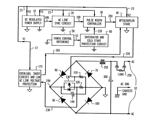
~ ~unct.ional system block diagram and .ircuit incorpor~t~
ing the -transistorized AC power controller is shown in Figure
1, comprising seven functional blocks operating in conjunction
with the AC power control block, shown in detail More ~-
particularly, a dual DC power supply lO provides the necessary
supply voltage for all cir~uitry involved in the process, :
i~cluding a sync signal on line 180 ~or an AC l.lne sync
circuit 20. The AC line sync circuit 20 generates a linear
descendant ramped.voltage in line 190 which is rese~ for each .:
AC line voltage zero crossing. Pulse width controller 30
compares the ramped voltage received on line 190 with a .-~
power control reference signal.received on line 210 from an .
integrator and cold start protection circuit 60. A power
control reference circuit S0 provides a DC reference
signal on line 52 which is processed by the integrator ancl
cold star~ protection circuit 60. Protection circuit 60 ~.
filters the reference voltage. of any spikes or other noise
that may generate errors in the pulse width controller,
thereby providing a usable power control reference signal on
line 210. Protection circuit 60 also-provides a fast zero
output power reset in case o a ~ault condition. The power
control reference signal on line 210 increases amplitude
slowly, to compensate for a slow settling time in applications
such as light dimming. For the same reason, the power
control reference signal's amplitude decrease speed is fast.
.::
At any tim~ when the value of the ramped voltage signal .~..
on line 190 is lower than the power control reference signal
on line 210,a comparator 402, to be described, provides on
6 - .
2 0 1 8 8 3 1
¦ line 200 a current pulse which turns on an optocoupler 40. -,
¦ If this event occurs, a volta~e pulse is applied on line 220 ~;
¦ to the gate of a power MOSFET 130. I.~ the load current sense ~.:
¦ signal on line 230 exceeds a preset value, the overload, short
¦ circuit and low AC line voltage protec~ion circuit 170 will ~-~
¦ turn off the load current and reset signal on line 210 to ;~
a zero value. Protection circuit 170 will perform the same
¦ function in the event of a low AC line voltage, to prevent
¦ the power MOSFE~ ~rom operating in a destructive linear ~:
¦ mode caused by insufficient amplitude of the gate drive pulse
¦ on line 220. :~
I ~ ~ ~
¦ Figure 2 shows the bridge rectifier connected to a bipolar
T I transistor 131 employed as the solid s-tate switch and repl~ces
' I the power MOSFET 130 shown and described with reference to
Figure 1. Here, the base of bipolar transistor 131 is
¦ connected to ~he output line 220 of optocoupler staye 40. ~rhe ~:
bipolar transistor 131 performs the same function 40 as the
power MOSFET 130. .~.
Figure 3 shows another alternate embodiment of the solid .~.
. ¦ s.tate switch wher~in a power sense FET 132 replaces the MOSFET
130 and the current sensing resistor 120 shown.and described
~ . with.reference to Figure 1. The power sense FET 132 is a
¦ conventional device comprising a.power MOSFET with built-in
I . current sensing capability. As shown in Figure 3, the drain
and souxce terminal of power sense FET 132 are connected.across
the direct current output of the.rectifier bridge. The gate
of power,sense FE~ 132 is connected.to.receive the output line
220 from optocoupler 40.
2 o ~ 8 8 3 ~
i ~ Figures 4.1 through 4.8 are electrical slgnal diagrams
for the lines indicated in such figures and described
above, thereby illustrating the operat.ing mode of the ::~
transistorized AC power controller.
:::
Figure 5 shows further details of the sys~ems block
elements described.and shown in con~ection w.i~h Figure l. :~
Dual DC power supply 10 is a conventional DC power supply
having a.transformer ll which receives an AC source via
lines 12 and provides the required voltage vl and v2 for
control circuits and drive, power and protection circuits,
as well as sync signal 180. Each DC power supply section
15 and 16.respectfully receives power from secondary -.
sections 13 and 14 and lS electrically isolated from the
other, by means of.their individual circuit grounds, shown by
respective ground symbols, and by isolated transformer second-
aries, so as not to endanger any external cixcuitry such
as remote control units or the operator. DC power supply j.
section 15 providos.a DC output vl on its output line 21
and, as detailed in Fig. 7, consists of a full wave
Schottkey.rectifier stage.17, and a diode 18 which separates
the output of s.tage 17 fro~ the voltage regulator and r.ipple
filter l9. DC power supply section 16 consists of a full
wave rectifier, a voltage regul:ator and a ripple filter, and ;.
supplies-power v2 on line 23 for the power stage drive
circuitry as well as the protection circuitry.
~:
The sync siqnal on line 180, as shown in Fig. 5, is
applied to the noninVerting input of a comparator 305 through :~
a network consisting of.resistors 300 and 301 and a zener
diode 302. The.role of.this network is to.reguIate the low :~
peak voltage of the full wave rectified voltage sync signal
on line 180. It will also protect the input of the comparator
305 against overvol.tag~. The thxeshold voltage is set by
a voltage divider comprising.resistors 303, 304. If sync
-8- ~-
~.
~l ~ ~
201~3:~
signal on line 180 drops below the threshol~ voltage, the
comparator's output sends a short duration voltage pulse to
the network consisting of a zener diode 306 and a capacitor
309, charging such capacitor 309 to a maximum voltage preset
by zener diode 306. Briclge rectifier stage 17 shown in
Fig. 7 consists of four Schottkey diodes: D~e to their low
I forward voltage drop, and a threshold voltage exceeding the
. low peak sync input voltage 180 by a small amount,there is prov
I a narrow output pulse from comparator 305. If the ~C line ~1
voltage is other than zero, no voltaye is applied on the network
306 and 309 by the comparator 305. There, the integrated
circuit 310, a constant current sink, that is, a discharge
current value set by resistors 311 and 312 and thermo-
compensated by diode 313, will discharge the capacitor 309
in a linear descendant ramp singal on line 190 to a value
above zero, for noise imunity if a remote power control
feature is required. Capacitor 307 will pre~ent any spurious
pulses at the output of comparator 305 due to switching
transients. Resistor 308 sets the optimum charge time and
the optimu~ bias current for zener diode 306.
¦ The linear descendant ramp signal on line 190 is applied
from the AC line sync circuit 30 to th~ pulse width controller
30 through resistor 400 to the noninverting input of
comparator 402~ If the amplitude of signal on line 190 drops
below the power control reference signal on line 210, comparator
402 will turn the internal LED of optocoupler 500 "on" via
line 200 and through the network consisting of resistors 404,
405 and capacitor 406, for a fast turn on/off. Capacitor
403 de-couples the power supply input of comparator 402.
1 ~ 201~31
To fur~her incre~se the output switchin~ spe-~1 of
3 optocoupler 40, resistor 502 is connected between its base an(7
emitter. ~esistor 501 sets the current in the op~ocouple~'s
~, output *ransistor and clamp transistor 504. Transistor 506
will increase the rate of the gate discharge of power MOSFET
130, if the gate is still charged with no input from the
optocoupler device 500. Resistor 110 will prevent excessive
~ate charge due to the capacitance between drain and gate
of MOS~ET 130. ~he actual AC power sw.itch consists of power
diodes 70, 80, 90, 100 in a bridge configuration and the
power MOSFE~. Metal oxide varistor 140 prevents any
destructive overvoltages across the power MOSFET. When the
~3, power MOSFET 130 is turned on, the voltage across it at
point 340 drops to zero or to a very low value, and the
output signal on sensing line 230 across current sense
resistor 120 increases. Resistor 120 has a value in the
range of from 5 to 20 milliohms.
In order to a~oid noise injection in the AC line, an
RFI filter consisting of inductor 150 and capacitor 160 is
provided, as shown in Figures 1, 2, 3 and 5. Inductor
150 is carefully selected, due to its additional function
of limiting the load current slew rate in the case of
an overload or short circuit. Two factors should be taken
into consideration when selecting the inductor 150. First, the
load current speed increase over the specified nonnal
operating range should be lower than the overall overload
. and short circuit protection loop response. This will
compensate for any delays in turning off the load current. This
; is shown by the load voltage increase signal across load 250.
The second factor to be considered is that the sa~uration
point on the BH curve should not occur unless a higher
current value than ~Imaximum before cut off'l is reached.
. .,
' -10-
2~33~ :
I :~ ~he power control reference circuit 50 provides the power
.~, control reference voltage on line 52 to the integrator and
cold start protection circuit 60 consisting of resistor
601 and Zener diode 602 in order.to li~lit its value below
; any destructive levels. The.time constant of.resistor 601,
resistor 603 and capacitor 605 will set the load current
i speed increase, due to larqe differences in the thermal lag
of different loads. If the power control reference voltage
on line 52 is lower than the voltage across the capacitor
605, the voltage at the base of transistor 604 is lower than
: its emitter's voltage, thereby turning the transistor on. ~
As a result, capacitor 605 will discharge rapidly to a :~:
voltage equal to the power control.reference voltage on
line S2. A slow load current turn on avoids any overload
conditions and wil~. not activate the overcu.rrent protection
circuit 170. A fast power control referenc~. voltage on line
52 will force a new slow load current turn on, if the load
current is externally restored.
~ .' . ' ~
~
Due to large differences in the thermal lag, as in the
case of light dimming applications, of different loads, the
decrease time of the control.referance voltage on line ~10
out of protection circuit 60 is much faster than the increase
time. This is designed to compensate for the slow load
settling speed and not activate the overload protection
circuit 170.
:
~ , .~"
201~831 ~
Ref~rring to Figure 6, the load current sense signal
on line 230 is filtered by resistor 800 and ca~acitor 801 of
the overload short circuit and low AC line vol~age protection
circuit 170 and applied to the inverting input of comparator
805. An overload/short circuit current limit.reference line
840 is set by voltage divider resistors 804 and 802. Capacitor
803 will filter this reference of any voltage spikes or other
noise. In the event of a load fault, such as an overload or
short circuit, where ~he load current is higher than a
pre-set value, the load sense signal 230, shown in Fig. 8.1,
will exceed the reference on line 84~, and comparator 805 will
send a "low" pulse 845 (Fig. 8.2) pulse to the trigger input .
pin T of timer 834. Capacitor 806 will decouple the DC - ~.
power supply voltage across comparator 805. The output o
timer 834 will turn high (Fig. 8.3) for a time "T" as set ~:~
by capacitor 809 and resistor 810, turning on clamp transistor
504 as shown in Fig. 5. Clamp transistor 504 is turned on
via resistor 811 by the signal on line 260 and will cut off
the voltage on the output o~ the optocoupler device 500,
(Fig. 8.4), the network consisting of resistors 5~3, 505, .
and .transistor 506 to thereby discharge the gate of the
power MOS~E~ 130 (Fig. 8.5), turning off the load current. "~
After time "T", the output of timer 834 will turn low again, ~.
and the load current will be.restored. ~hen timer 834 is .. :;~
triggered, timer 827 is also .triggered via common connection ~
841 and its output.turns high for amounts larger than (i ~ 1) .:.
"T", turning on.*ransistor 832 throùgh.resistor 833. This
will change the.vol.tage on the reset input of counter 814 to .. ~
zero. The oounter.reset pin is kept high through resistor 822, .:`
Zener diode 821 and.resistor 815. As a result, the resat
function is disabled, and the counter 815 is able to start
counting pulses.
-12- ;
~,
~ . 20~3~ ~
As shown in Figure 6, the output of timer 834 will also
apply high pulses to the clock input (Ck) of counter 814 through
resistor 812 and will turn transistor 818 on through resistor
i819. Transisto~ 818 will simulate a low D.C. power supply
voltage and turn transistor 823 off, and such transistor 823
wi].l turn off the relay 825. Relay 825 consists of its coil
as shown at 825 which activate the contact switches 507 and
607, shown in Figure 5 in the of position. The turning off
of relay 825 (Fig. 8.6) disconnects the power MOSFET's gate
via line 220 and the power control referellce voltage 210.
Relay 825 may be replaced by a dual optocoupler or other
solid state switch, not shown, with ~inor circuit modifications.
.-:.'
After time "T", the output (out) of timer-834 will turn
low, transistors 504 and 818 will be turned off, as shown in
~igures 5 and 6, and the load current will be restored. If the
fault persists, the output o comparator 805 will send a new
low pulse 847 (Fig. 8.2) to timer 834, turning its output
high for another time "T" ~Fig. 8.3). Counter 814 will
receive a new clock pulse, counting it. ~ransistor 818 will
be turned on again, simulating a new D.C. power supply malfunc-
tion or a low A.C. line voltage. As a result, relay 825
will be t~lrned off again (Fig . 8 . 6) by transistor 823 . Timer
827 had been triggered by the first fault cycle, transistor
832 is still on, and the counter reset ~unction is o (Fig. 8.7
:
If, after the~ 1) number of ault cycles, the overload
or short circuit condition still persists, the Qi output of
counter 814 becomes high, thereby turning transistor 817 on.
Transistor 817 will act identically to transistor 818, turning
! transistor 823 and relas~ 825 off. This will not permit an auto-
¦¦ matic restorat of load current, since no new feult oycles are
-13-
;~
.~ , .
li l ~ 2~g~3~
possible. The output state of counter 814 cannot be changed
unless a new pulse is applied to the clock lnput or reset
switch 820 (Fig. 8.8) applies a positive vol~a~e to the
reset input ~ of counter 814 via resistor 831. The manual
reset is possible only after time (i ~ l)T, when transistor
832 is off, thereby allowing the presence o positive
voltage on the reset input R of counter 814. ~3efore time
(i + l)T, the automatic reset function is disabled by
transistor 817 which has been latched on.
If, after time ~i + l)T ~rom a fault event, the load
current stays on, the output of timer 827 becomes low, and
transistor 832 tùrns of, thereby resetting the counter 814.
The circuit values determining the time (i + 1) T are chosen
to reset the counter for non~repetitive faults.
If the A.C. line voltage drops below a certain value,
the D.C. supply voltage V2 becomes too low, forcing the power ~-
~MOSFET 130 to operate in a destructive linear mode. In the
system o the pre~ent invention, as shown in Figure 6, i~ the ~-
~D.C. supply voltage V2 drops below the voltage of Zener diode
824, the transistor 823 will turn off, thereby turning
off the relay 825 and disconnecting the power control reference
voltage 210 via relay contact 607, as shown in Figure`5. In
this manner, the power MOSFET 130 is protected from
destruction.
-14-
~1 20~
I
¦ In general, the operation of the A.C. power controll~r
¦ is summarized as follows. The A.C. line voltage on line 12 cross
¦es the zero crossing 120 times per second. For each crossinq, th,
¦capacitor 309 in the A.C. line sync circuit 20 is charged to a
pre-set voltage, and then discharged to a "V" value, above zero,
¦ for noise immunity, by the constant current sink circuit incluclin~ ~-
¦ ¦capacitor 309, integratec] circuit 310, resistors 311 and 312,
¦ and diode 313 in the ~.~. 'line sync circuit 20. As a result,
¦the output line lg0 is a linear descendant ramp that is reset
or each A.C. line voltage zero crossing. Next, the descendant
, ¦ ramp vo~tage on line 190 is applied to the pulse width controller
30 where it is compared with the po~er reference control signal
¦ on line on line 210'to provide the pulse width control signal
on line200. If the descendant ramp voltage on line 190 becomes
lower than the reference voltage on line 210, the optocoup'ler
¦ `500 is turned on b~ the pulse width signal on line 200 out of
~l the comparator 402.' This latter operation is the primary functio~
of the ~ulse width controller'30.
The output transistor 506 of optocoupler stage 40
wlll charge the gate of the po~er MOSFET 130 up to a voltage of
over 10 volts, turning it on. MOSFET 130 is forward connected
diagonally to to the D.C. output 240 of the rectifier bridge.
The A.C. input of the bridge is similar to a switch terminal.
To avoid any damage due to high voltage transients, the metal
, oxide varistor 140 is connected across the power MOSFET 130.
An RFI LC filter consisting of inductor 150 and
capacitor 160 is connected between the load 250 and rectiier- '~
switch combination to thereby reduce any possible switching noise
in the A.C. line. ~nductor 150'also fùnctions to limlt the load '
current slew rate in case of an overload or short circuit.
'.,
~ -15-
I 2 ~
I . ~.
¦ If, due to large AC voltage varlations, the Vl and
¦ V2 voltages on lines 21 and 23 dro~ below a c~rtain safe
¦ level, which would pu~sh the power MOSF~T 130 into ~ destructive
¦ linear mode, the MOSFET gate is disconnected from the driver
¦ stage and discharged. Also, the control reference voltage on
¦ line 210 is cut off. As stated above, the re~erence
recovery time is much longer than the decay time, if all
¦ faults are clear.
~, I ..
If the load current at 250 exceeds a preset value on ;~
line 840, the comparator 804 in overload circuit 170 will
send a "low" pulse to the timer circuit 834 set for one
second. The output of the timer 834 turns on the driver ~
clamp transistor 504 which turns the MOSFET gate voltage to ~;
zero. ~t the same time, the cornparator 805 sends a pulse to
counter 814. After T seconds, the load current 250 will
reset. If the ~ault still exists, a nsw timing cycle will ~-
begin and a second pulse will be sent to the counter 814.
A~ter "(i+l)" number of attempts to restore the load current, -~
if the fault still exists, the counter 814 output will
permanently shut the optocoupler drive circuit off, requiring
system troubleshooting and manual reset. For example, ~-
if after the second cycle, the fault such a~ a temporary short
circuit caused by a lamp burnout, is terminated, the system
will operate normally since the counter 814 will be automatical]
reset to zero after (i~l)T seconds. Therefore, no permanent
shut of~ will take place.
,,
In the system of the present invention, the load current
shut ofE time is extremely short, in a range of a few micro-
seconds,-protecting the power control devices 130, 131 or 132
against self destruction if maximum load current is exceeded.
. ,.-
. '.. .. '''
-16-
2018831
It also provides~a presentl.~ not.texisting safety feature in
any commercia~l industrial, hazardous and military AC ..
power appl.ications. It provides pro-tection against expensive
self des.truction, expensi.ve bullding repa.ir in case of fire
caused by short circUit. ~ provides protection against
loses of human lives caused by fire, exploc;ion or other
electric xelated accidents.
While the invention has been described above w.ith respect
to its preferred embodiments, it should be understood that
other ~orms and embodimehts may be made without departing
from the spirit and scope of the present invention.