Note: Descriptions are shown in the official language in which they were submitted.
NE-265 20188~5
TITLE OF THE INVENTION
2 "Burst Demodulator For Establishing Carrier and Clock Timing From A
3 Sequence of Alternating Symbols"
4 BACK~;ROUND OF THE INVENTION
s The present invention relates generally to digital communications
6 systems, and more specifically to a technique for recovering carrier and
7 clock timing for burst signaJ demodulation.
8 Synchronous detection technique has been extensively used for
9 demodulating amplitude-phase shift keyed (APSK) signals to take
advantage of its relatively high power efficiency by recovering carrier
11 phase and clock (symbol) timing. When the signal is of a bursty nature,
12 the carrier and bit timing recovery must be accomplished in a short
13 period of time in response to the arrival of each burst. It is the usual
14 practice to append a preamble containing a carrier recovery sequence
and a clock recovery sequence to the header of each burst. The
16 preamble comprises a nonmodulated portion (all 1 's or all -1 's) for carrier17 recovery and a modulated portion which is a sequence of alternating 1's
18 and -1's for clock recovery. Since the preamble is an overhead that
19 tends to decrease the transmission efficiency, or throughput of the digital
20 communication system, it is desired that the length of a preamble be as
21 short as possible.
22 A technique has been proposed to eliminate the need of a preamble
23 as discussed in "Preambleless Demodulator for Satellite Communi-
24 cations", H. Tomita and J. Namiki, 1989, IEEE (CH26S5-9/89/0000-S04).
2S According to the proposed technique, a substantial amount of
26 information symbols is required for symbol timing and carrier recovery.
27 To establish synchronization in as short a period of time, very high-
28 speed computation capability is required. Furthermore, at the present
N E-265
2~188~
- 2 -
state of technology, the proposed system results in costly hardware
2 implementations.
3 SUMMARY OF THE INYENTION
4 It is therefore an object of the present invention to increase the
5 throughput of a digital communications system.
6 Another object of the invention is the use of a preamble which
7 comprises a single sequence-of alternating 1's and -1's for both carrier
8 phase and symbol timing recovery.
9 The present invention provides a burst demodulator which comprises
10 an orthogonal detector for receiving an amplitude-phase shift keyed
11 (APSK) burst signal containing a preamble of alternating "1" and ~_1N
12 symbols, and a data field. The detector quasi-coherently demodulates
13 the received burst signal into a baseband complex signal, which is
14 converted to digital form in such a way that each symbol of the complex
15 signal yields N binary-coded digital samples, where the integer N is
16 selected such that at least one of the N digital samples is closest to a
17 signal point of the received burst signal. A burst detector is provided for
18 detecting the arrival of the burst signal. A clock recovery circuit is
19 responsive to the detection of the arrival of the burst signal for estimating
20 the symbol timing of the burst signal from digital samples of the
21 preamble. A digital sample is extracted from every N samples of the
2 2 preamble in response to the estimated symbol timing so that the
23 extracted sample is most likely to be closest to the signal point. A carrier
24 recovery circuit responds to the estimated symbol timing by estimating
25 the carrier frequency and phase of the burst signal from the extracted
26 digital samples to produce a complex carrier signal, which is multiplied
27 with the extracted digital samples to recover the original signal.
28 In a preferred embodiment, memories are provided to store the
NE-Z~5 20188~5
received burst signal. By repeatedly addressing the memories, clock
2 timing and carrier phase recovery operations are performed in
3 succession on the same symbols of the preamble.
4 It is preferred that the burst detector comprises a preamble generator
for generating a local sequence of alternating "1 " and U-1n symbols. The
6 "1" symbol of the local sequence is multiplied with N samples of first
7 occurrence and the "-1 " symbol of the local sequence is multiplied with N
8 samples of subsequent occurrence. The multiplied samples are split into
9 a sequence of odd-numbered samples and a sequence of even-
numbered samples and low-pass filtered. A first absolute value of the
11 lowpass-filtered odd-numbered samples and a second absolute value of
12 the lowpass-filtered even-numbered samples are determined and
13 respectively lowpass filtered. A combined absolute value of the lowpass
14 filtered odd- and even-numbered samples is determined and compared
15 with a predetermined threshold value. If it exceeds the threshold value, a
16 signal indicating the arrival of a burst signal is generated.
17 BRIEF DESCRIPTION O THE DRAWINGS
18 The present invention will be described in further detail with reference
19 to the accompanying drawings, in which:
Fig. I is a block diagram of an APSK burst demodulator according to
21 a first embodiment of the present invention;
22 Fig. 2 is a timing diagram showing read times of the random access
23 memories of Fig. 1 with respect to the preamble of a received burst
24 signal;
2S Fig. 3 is a block diagram of the burst detector of Fig. 1;
26 Fig. 4 is a waveform diagram associated with the burst detector;
27 Fig. 5 is a block diagram of an example of the clock recovery circuit
28 of Fig. 1 ;
NE-265 2 ~ 1 8 8 ~ ~
- 4 -
Fig. 6 is a block diagram of a preferred clock recovery circuit;
2 Fig. 7 is a block diagram of the carrier recovery circuit of Fig. 1;
3 Fig. 8 is a block diagram of a second embodiment of this invention;
4 and
s Fig. 9 is a block diagram of a third embodiment of this invention.
6 DETAILED DESCRIPTIQN
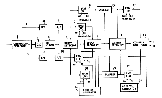
7 Referring now to Fig. 1, there is shown an APSK (amplitude-phase
8 shift keyed) burst demodulator. The demodulator comprises an
9 orthogonal detector 1 of conventional design for receiving APSK burst
signals from a transmitter. Each burst signal contains a preamble having
11 a sequence of alternating symbols 1 and -1, followed by a data field as
12 shown in Fig. 2. Orthogonal detector 1 is supplied with quadrature
13 carriers from a local oscillator 2 and detects the in-phase and guadrature
14 components at baseband frequencies from the received burst. Since the
15 local oscillator 2 is not synchronized with the carrier phase of the
16 received burst, the detection in this manner is in a 'quasi-coherent mode',
17 i.e., the incoming signal is 'coarsely' demodulated. Therefore, the quasi-
18 demodulated baseband signals contain a phase difference between the
19 local and transmitted carriers and ~his phase difference will be
20 compensated for at a later stage.
21 The in-phase and quadrature components are supplied respectively
22 on an l-channel path and Q-channel path to low-pass filters 3i and 3q to
2 3 remove their high frequency components in order to restrict the
24 baseband signals below the Nyquist frequency. The outputs of LPF 3i
2S and 3q are respectively fed to A/D converters 4i and 4q and sampled in
26 response to a pulse supplied from a high-frequency clock generator 5 at
2 7 an integral multiple (N) of the original sampling rate so that each
28 incoming symbol yields N analog samples. Each of the N analog
NE-2~5 20188~5
samples is converted into an n-bit digital sample of complex value. The
2 integer N is so selected that at least one of the N samples is closest to a
3 signal point. The output of A/D converter 4i is supplied to one input of a
4 burst detector 6 as well as to random access memories 7i and 8i, and the
s output of A/D converter 4q is supplied to the other input of burst detector
6 6 as well as to random access memories 7q and 8q. The read/write
7 operations of random access memories 7i, 7q) 8i and 8q are controlled
8 by an address generator 14. Each of these RAMs is of dual port type
g which allows simultaneous write and read operations. Address generator
10 14 continuously supplies a sequence of write addresses W1 to RAMs 7i,
11 7q, 8i and 8q to store digital sarnples from the A/D converters. Address
12 generator 14 generates two sequences of read address signals R1 and R2
13 for reading RAMs 7i, 7q and RAMs 8i and 8q, respectively. In response
14 to the output of burst detector 6 which may occur at time t1, address
15 generator 14 resets its read address signal R1 to an initial address count
16 which is equal to the current write address minus a prescribed address
17 count which corresponds to a delay time T1. This prescribed address
18 count is so determined that read operation may begin with symbols
19 which were stored in RAMs 7i, 7q at burst arrival time to. In this way,
20 RAMs 7i and 7q delay the preamble by time period Tl with respect to
21 the burst arrival time to.
22 The Tl-delayed samples of the preamble from RAMs 7i and 7q are
23 fed to respective inputs of a clock recovery circuit 9 to which the output
24 of burst detector 6 is also applied. Thus, clock recovery circuit 9 is now
2S able to perform a clock recovery operation beginning with the first
26 symbol of the preamble. On establishing clock synchronization, clock
27 recovery circuit 9 generates a sequence of clock pulses which are fed as
2~ sampling pulses to samplers 10i and 10q to which the outputs of RAMs 8i
NE-265 20188~5
- 6 -
and 8q are respectively applied when the eye opening of the incoming
2 signal is at the largest.
3 Address generator 14 is further responsive to the clock pulse of first
4 occurrence, which may be supplied from clock recovery circuit 9 at time
S t2, to reset its second read address signal R2 to an initial address count
6 which i5 equal to the current write address minus a prescribed address
7 count which corresponds to a delay time T2 from burst arrival time to.
8 This prescribed address count is also determined that the read operation
9 with address sequence R2 may begin with symbols which were stored in
l o RAMs 8i, 8q at burst arrival time to. In this way, RAMs 8i and 8q delay
11 the preamble by time period T2 with respect to the burst arrival time to.
12 The T2-delayed symbols of the preamble from RAMs 8i and 8q are
1 3 respectively sampled by samplers 1 0i and 1 Oq in response to the
14 sampling pulse from clock recovery circuit 9 so that in each of these
samplers a most likelihood sample is chosen from every N samples.
16 The outputs of samplers l Oi and 10q are fed to respective inputs of a
17 carrier recovery circuit 11 as well as to RAMs 1 2i and 1 2q, respectively.18 The read/write operations of RAMs 12i and 12q are controlled by an
1 9 address generator 15 which, in a manner similar to address generator 14,
continuously supplies a sequence of write addresses W2 to RAMs 1 2i and
21 1 2q to store the outputs of samplers 10i and 10q. Address generator 15
22 responds to the output of carrier recovery circuit 11, which may occur at
23 time t3, by resetting a sequence of read addresses R3 to an address
24 count which is equal to the current write address W2 minus a prescribed
25 address count which corresponds to a delay time T3. This prescribed
26 address count is so determined that read operation of RAMS 12i, 12q
27 may begin with symbols which were stored in these RAMs at burst arrival
2 8 time to-
NE-265
~$1~8~
- 7 -
In this way, RAMs 1 2i and 1 2q delay the preamble by time period T3
2 with respect to the burst arrival time to and carrier recovery operation is
3 effected on the same sequence of alternating "1" and "-1" symbols of
4 the preambie as those on which the burst detection and clock recovery
s operations were performed. The outputs of RAMs 1 2i and 1 2q are fed to
6 respective inputs of a product demodulator, or complex multiplier 13.
7 Carrier recovery circuit 11 responds to the output of clock recovery circuit
8 9 indicating the recovery of a clock by starting a carrier recovery
9 operation in which it estimates the carrier frequency and phase from the
10 oùtputs of samplers 10i and 10q and supplies a carrier frequency and
11 phase output in complex value to complex multiplier 13. In multiplier 13,
12 it is used to coherently demodulate delayed digital sarnples from RAMs
13 12i, 12q to generate a replica of the original l-channel and Q-channel
14 signals.
It is seen that the same preamble of alternating "1" and "0" bit
16 sequence is successively delayed for use in burst detection, clock
17 recovery and carrier recovery operations, thus allowing the system to
18 establish carrier and clock synchronization with a short-length preamble.
19 Details of burst detector 6, clock recovery circuit 9 and carrier
recove~ circuit 11 will now be described with reference to Figs. 3 to 7.
21 In Fig. 3, burst detector 6 is shown as comprising a preamble
22 generator 20 which generates a sequence of alternating values "1" and
23 "-1" at 1/N of the original sampling rate and supplies it to multipliers 21i24 and 21 q to which the outputs of A/D converters 4i and 4q are
respectively applied. Thus, every N digital samples of the received
26 preamble are multiplied with "1" or "-1" by multipliers 21i and 21q to
27 produce a sequence of samples with a value "1". If the phase timing
28 precisely matches the incoming signal, all samples of the preamble will
NE-265
2a~88~
- 8 -
be transformed to values "1" so that the outputs of multipliers 41i and
2 41q appear as if ~he carrier were unmodulated during the preamble. In
3 this case, the modulating signal is substantially removed from the
4 preamble, extracting the carrier components at the outputs of multipliers
S 21 i and 21 q for enabling the burst to be detected.
6 Since the preamble generator 20 is not synchronized with the
7 incoming signal, all samples of a preamble are not necessarily converted
8 to all 1's. The outputs of multipliers 21i and 21q are supplied to sarnplers
9 22i and 22q, respectively. Each sequence of N samples from multiplier
10 21 i is sampled by sampler 22i at twice the original sampling rate (or 2/N
1 1 of the clock rate of generator 5) to yield two output samples from every
12 N input samples. One of these samples is supplied as a sequence of odd-
13 numbered samples S2k 1 or sine signals to a low-pass filter 23i and the
14 other is supplied as a sequence S2k of even-numbered samples or cosine
15 signals to a low-pass filter 24i twhere k = 1, 2, 3 ...). Likewise, every N
16 samples from multiplier 21 q is sampled at twice the original sampling rate
17 by sampler 22q to extract two samples from every N samples and one of
1 8 which is applied to a low-pass filter 23q as an odd-numbered sample and
19 the other of which is applied to a low-pass filter 24q as an even-
20 numbered sample.
21 The effect of low-pass filters 23i, 24i, 23q and 24q is to remove high-
22 frequency noise components of the sampled sequences. The outputs of
23 low-pass filters 23i and 24q are coupled to envelope detectors 25i and
24 25q, respectively, and the outputs of low-pass filter 24i and 23q are cross-
2S coupled to envelope detectors 25q and 25i, respectively. Each of these
26 envelope detectors 25i and 25q produces an output representative of the
27 absolute value of the inputs. Since the input signals are of complex
28 signals, each envelope detector calculates ~(S2k-1)2+(S2k)2, or square
NE-265 2al88~i
g
root of the sum of the squared real and imaginary components. The
2 outputs of envelope detectors 25i and ~Sq, if represented by analog
3 form, would appear as a sequence of half-wave pulses of "quasi-
4 sinusoid" as shown in Fig. 4 due to the rolloff characteristics of the low-
S pass filters 3i and 3q. Each of these half-wave pulses arises from
6 components S2k 1 and S2k sampled at times t1 and t2. The variance of
7 the outputs of envelope detectors 25i and 25q is then reduced by low-
8 pass filter 26i and 26q, whose outputs are coupled to an envelope
9 detector 27 which calculates the root-sum-square value of its input
1 0 samples.
11 Since the outputs of envelope detectors 25i and 25q are of quasi-
12 sinusoid of half-period waveform, the sampled data S2k l and S2k can be
13 considered as orthogonal to each other, and hence, the calculation of
14 the root-sum-square value of these signals by envelope detector 27
15 results in the generation of a large amplitude envelope comparable to
16 one which would be derived from the transmitted signal point. In
17 addition, each of the values of envelopes S2k 1 and S2k is not necessarily
18 at maximum due to the phase difference between the locally generated
19 preamble and the received one. Thus, when envelope detector 25i
20 produces a maximum amplitude output, the other detector 25q would
21 produce a minimum amplitude output. Therefore, the splitting of the
2 2 carrier component by samplers 22i and 22q into sine and cosine
23 components and the root-sum-square calculation of envelope detector
24 27 can result in a constant amplitude output, compensating for the phase
2S difference between the received preamble and the one produced by
26 local preamble generator 20.
27 A comparator 28 is coupled to the output of envelope detector 27. If
2 8 the output of envelope detector 27 exceeds a reference value,
NE-265
~0~885~
10 -
comparator 28 generates an output signal indicating the arrival of a burst.
2 It is to be noted that in an alternative embodiment each of the envelope
3 detectors 25i, 25q and 27 provide calculation of the sum of squares,
4 instead of the root-sum-square calculation.
s As shown in Fig.5,clock recovery circuit 9 is made up of an envelope
6 detector 30, an orthogonal detector 31, low-pass filters 35i, 35q and a
7 arctangent calculator 36. Envelope detector 30 calculates the root-sum-
8 square value of the outputs of RAM 7i and 7q and applies a complex
9 output signal to orthogonal detector 31. Orthogonal detector 31
comprises a read-only memoly 33i which stores data indicating the
11 products of phase values of a sinusoid and input sine components which
12 will be generated by envelope detector 30 and a read-only memory 33q
13 which stores data indicating the products of phase values of a cosinusoid
14 and input cosine components. ROM's 32i and 32q are respectively driven
1 S by counters 32i and 32q which are clocked a high frequency rate. The
16 complex signal from envelope detector 30 is applied to multipliers 34i
17 and 34q and multiplied with the outputs of ROMs 33i and 33q. The
18 outputs of multipliers 34i and 34q are supplied to low-pass filters 35i and
19 35q, respectively, as orthogonally detected signals.
20 Arctangent calculator 36 is enabled in response to the output of burst
21 detector 6 to calculate the arctangent of the outputs of low-pass filters 35i22 and 35q to produce a signal indicating the phase angle, or clock timing
23 of the symbols contained in the preamble. The output of arctangent
24 calculator 36 is thus caused to appear when the eye opening of the
25 incoming signal is at the largest, and applied as a sampling pulse to
26 samplers 10i and 10q, so that a digital sample extracted by each of these
27 samplers is one that is closest to the transmitted signal point.
28 In Fig. 6, a preferred form of the orthogonal detector is shown at 31'
N E-265
2~188~
11
as comprising a sampler 37 and subtractors 38 and 39. Sampler 37
2 provides sampling on every N input samples at four times the original
3 sampling rate to extract four samples from every N input samples and
4 split them into successive sample sequences S ~k-3, S 4k-2, S 4k-1 and S 4k-
5 Since the output of envelope detector 30 contains the modulating
6 component of quasi-sinusoid, samples S'4k 3 and S'4k 2 can be regarded
7 as quasi-demodulated complex signals, while samples S'4k 1 and S'4k can
8 be regarded as DC and harmonics components which result if the
g bandlimiting of low-pass filters 3i and 3q is not sufficient. To remove
10 these undesired components, samples S'4k 1 and S'4k are subtracted from
11 samples S'4k 3 and S'4k 2 by subtractors 38 and 39 to produce outputs for
12 coupling to low-pass filters 35i and 35q, respectively.
13 Fig. 7 shows details of the carrier recovery circuit 11 of Fig. 1. As
14 illustrated, carrier recovery circuit 11 includes a preamble generator 40,
15 multipliers 41 i and 41 q, DFT calculators 42-1 through 42-N, a
16 freguency/phase estimator 43, and a numeric controlled oscillator 44.
17 Multipliers 41i and 41q extract carrier components from the outputs
18 of samplers 10i and 10q. Preamble generator 40 is responsive to the
19 output of clock recovery circuit 9 to supply a value "1 " to multipliers 41 i20 and 41q for multiplication with samples "1'~ of the preamble extracted by
21 samplers 10i and 10q and is responsive to the next clock input to supply a
22 value "-1" to multiply it with samples "-1". In this way, quadrature
23 carrier components completely free of modulating components are
24 available at the outputs of multipliers 41i and 41q. A plurality of DFT
2S (discrete Fourier transform) calculators 42-1 to 42-N are provided. Each
26 DFT calculator includes a rotator 45, an accumulator 46, a RAM 47 and a
27 ROM 48. The multipliers 41i and 41q are coupled to the rotator 45 of
2 8 each DFT calculator 42 where their outputs of complex value are
N E-265
2~188~
- 12 -
multiplied with phase angle values supplied from ROM 48 in response to
2 a timing signal from a timing circuit 49. The outputs of rotator 45 are fed
3 to accumulator 46 to calculate the following equations:
4 Fk = ~ Xn exp(-j27~ N
Bk = ~;/2X;~-exp( j2~ N
6 where Xn represents the input samples from rotator 45.
7 The outputs of accumulator 46 are stored in RAM 47 and thence to
8 frequency/phase estimator 43. Estimator 43 first determines the absolute
g value of Fk + Bk and then determines k which maximizes the absolute
10 value, and finally determines frequency ~ and phase ~ by calculating the
1 1 following equations:
1 2 ~ = 0. 5 f k + 11 (Arg(Fk) - Ar~(Bk ))
13 ~ = 0.5 (Arg(Fk)-Arg(Bk))
14 The frequency and phase outputs of estimator 43 are supplied to
15 numeric controlled oscillator 44 to generate a replica of the transmitted
16 carrier for coupling to the complex multiplier 13.
17 Carrier recovery circuit 11 of the type described above is particularly
18 suitable if the incoming burst is of a short duration containing as small as
19 a few hundreds symbols. However, a carrier phase error occurs due to
20 inherent frequency estimation error caused by carrier recovery circuit 11
21 at the beginning of a burst. While it can be tolerated for short duration
22 bursts, the initial phase error increases as demodulation proceeds toward
23 the end of the burst, leading to an unfavorable situation in the case of
24 long duration bursts.
2S Fig. 8 shows a second embodiment of the present invention which is
26 suitable for demodulators handling burst signals containing a long data
'
NE-265 2~ g~
- 1 3 -
1 field or a variable length packet. In this embodiment, the burst
2 demodulator additionally includes a second carrier recovery circuit 50 of
3 a phase-locked loop type which differs from the first carrier recovery
4 circuit 11 in that it maintains synchronization indefinitely after its has been
s established by continuously tracking the carrier phase. A counter 51 is
6 connected to the output of burst detector 6 to start counting in~ernal clock
7 and feeds a switching pulse to a switch S2 when a prescribed amount of
8 time has elapsed following the detection of a burst signal. Switch 52 is
9 initially positioned to the left for coupling the output of the firs~ carrier
10 recovery circuit 11 to complex multiplier 13.
l 1 As illustrated the second carrier recovery circuit 50 comprises a
12 phase detector 53 coupled to the outputs of complex multiplier 13, a
13 loop filter 54 which applies the output of phase detector 53 to a numeric
14 controlled oscillator 55. Numeric controlled oscillator 55 is also supplied
15 with a signal indicating the frequency and initial phase values of the burst
16 signal estimated by the first carrier recovery circuit 11 to continuously
17 generate a complex carrier signal. In response to a switching pulse, the
18 transfer contact of switch 52 is moved to the right, and the carrier
19 recovered by the second carrier recovery circuit 50 is fed to complex
20 multiplier 13. In this way, a phase-locked loop is formed by carrier
21 recovery circuit 50 and complex multiplier 13 to maintain the phase-
2 2 locked carrier generation.
23 Fig. 9 shows a third embodiment of the present invention in which
24 parts corresponding to those in the previous embodiments are marked
25 by the same numerals as used therein. A burst detector 60 of the type
26 identical to that shown in Fig. 3 and a clock recovery circuit 61 of the ~ype27 shown in Fig. 5 are connected to the outputs of A/D converters 4i, 4q,
2 8 and random access memories 62i and 62q of dual port type are
N E-265
~188 .~
- 14 -
connected respectively to the outputs of A/D converters 4i and 4q. An
2 address generator 63 constantly supplies a write address to RAMs 62i,
3 62q to store digital samples from A/D converters 4i, 4q. Upon detection
4 of a burst at time t1, burst detector 60 supplies a signal to address
s generator 63 to cause it to initialize its read address which is displaced by
6 a predetermined amount of address counts from the current write
7 address, so that the initial read address can access the locations o~ RAMs
8 62i, 62q in which the digital samples at the beginning of a preamble are
9 stored. Clock recovery circuit 61 is triggered in response to the output of
10 burst detector 60 to start hunting clock timing. Clock pulses are
11 generated by clock recovery circuit 61 and supplied to address generator
12 63 to cause it to successively increment its read address. Therefore,
13 digital samples of the preamble are read out of RAMs 62i and 62q at the
14 instant at which the eye opening of the incoming signal is at the largest.
15 The samples read out of memories 62i and 62q are supplied to a DFT
16 calculator 64 and a phase-locked loop 65 which forms a carrier recovery
17 circuit with DFT calculator 64. The latter performs discrete Fourier
1 8 transform on every N samples from the memories 62i, 62q and estimates
19 the frequency and initial phase of the residual carrier of the received
20 burst signal.
21 On completion of a DFT calculation at time t2, calculator 64 supplies
22 signals indicating the estimated carrier frequency and phase to phase-
23 locked loop 65 to initialize its parameters to allow it to subsequently
2 4 generate a carrier signal of complex value. Simultaneously, DFT
25 calculator 64 supplies a signal to address generator 63 to reset its read
26 address to the initial value. Therefore, digital samples of the preamble
27 are again read out of memories 62i and 62q and supplied to a complex
28 multiplier 66 as well as to phase-locked loop 65. In the phase-locked
NE-265
2,~188~
- 15 -
loop 65, it is used to continuously generate the complex carrier signal
2 having the estimated frequency and phase and applies it to complex
3 multiplier 66 to precisely detect the digital samples to recover a replica of
4 the original l-channel and Q-channel signals. After the first DFT
calculation, calculator 64 no longer supplies a reset signal to address
6 generator 63 to allow it $o simply perform write and read operations for
7 data field that follows.
8 The burst demodulator of this invention can be advantageously
9 implemented by using digitial signal processing techniques.
The foregoing description shows only preferred embodiments of the
11 present invention. Various modifications are apparent to those skilled in
12 the art without departing from the scope of the present invention which is
13 only limited by the appended claims. Therefore, the embodiments
14 shown and described are only illustrative, not restrictive.