Note: Descriptions are shown in the official language in which they were submitted.
2 0 ~8 97 ~
... ~ -.,. . -.
DOPING PROCEDURES FOR SEMICONDUCTOR DEVICES
Technical Field
... . ~, ...
The invention is a process for making various semiconductor devices,
both electronic and optical and the devices made by such processes.
5 Back~round of the Invention -
Semiconductor device technology has undergone explosive development
in recent years. Many new semiconductor devices have been developed,
characteristics of known devices have been va$1y improved and device integrationhas continued to be improved. With regard to device integration, packing densities
10 continue to increase and multifunction integrated devices (e.g., optoelectronic
devices such as PINFETs) continue to be developed.
A particularly different problem in semiconductor device technology is
precise con~ol of doping profiles in the semiconductor materials. Precise dopingprofiles improve device characteristics and permit greater packing density for
15 various devices (e.g. memory devices, logic devices, etc.). For example, with field
effect Transistors, precise confinement of the dopants to the doping region improves
such characteristics as cut-off voltage, gain characteristics and transconductance.
With semiconductor heterojuncdon lasers, precise confinement of the doping profile
to the barrier layer improves various laser characteristics such as threshold cuTrent, ~ ~ ;
20 power output etc.
A particular problem with obtaining desirable doping profile is the
redistribution of dopants occurring during crystal growth. It is highly desirable to
limit these redistribution effects so as to be able to control the doping profile
obtained in semiconductor devices. p;
A variety of mechanisms contribute to redistribution effects including ;
diffusion of dopant ions, segregation effects of dopant ions, etc. Segregation effects
refer to the movement of dopant ions toward the surface of the serniconductor.
Segregation effects are mentioned in a number of publications. In one reference
(Crystal Growth of Bulk Crystals: Purification, Doping and Defects by ;
30 A. J. R. DeKock; Handbook _ Semiconductors, Volume 3, S. P. Keller ed, North-
Holland, New York, 1980, Cha. 4, especially Page 251) segregation effects are used ~ ~
to explain the purification technique known as zone refining. Also, in a paper by;; ~ ~;
A. Y. Cho ((Impurity Profiles of GaAs Epitaxial Layers Doped with Sn, Si, and Ge ` ;
Grown with Molecular Beam Epitaxy, Journal f Applied Physics, Volume 46, No. 4 ; `
35 April 1975), surface segregation effects are used to explain certain doping pro iles ~ `~
obtained from crystal structures made by molecular beam epitaxy.
:,'~ .,`,'','`.'
-~ 20 1 8976
-2
Indeed, segregation effects play a particularly important role with a
number of dopant species which would otherwise be used more extensively. For
example, tin and zinc have certain veIy desirable doping characteristics for III-V ;
semiconductor compounds such as gallium arsenide including high specificity to
S particular doping site. However, segregation effects exhibited by these dopant ions
severely limit the use of these dopant ions. Particularly desirable is a procedure which
would reduce or eliminate segregation effects and permit fabrication of semiconductor
devices with sharp, well defined doping profiles.
Summar~ of the Invention ~ -
The invention is a process for fabricating semiconductor devices
comprising semiconductor material with a highly controlled, precise doping profile. ;~
Unique in the process is a crystal growth procedure which minimizes or eliminates the
effects of Fermi-level pinning on the doping profile of the semiconductor material.
The crystal growth procedure includes steps to screen the dopant ions from the surface
electric fields set up by Fermi-level pinning, reduce or eliminate Fermi-level pinning or
minimized or eliminate redistribution of dopants due to surface electric fields.Particularly convenient is illumination of the growth surface so as to create electron-
hole pairs to shield the surface electric field from the dopant ions. Also useful is `
background doping to screen the dopant ions from the surface electric fields resulting
from Fermi-level pinning. Another procedure is providing crystal growth on crystal
surfaces where there is no Fermi-level pinning or where only weak electric field are
created by Fermi-level pinning. Also, the effects of the surface electric fields created
by Fermi-level pinning are minimized by carrying out the crystal growth process at ~ ~ ~
unusually low temperatures where dopant ion redistribution effects are small. ;
Combinations of the above procedures are also useful. Unique semiconductor devices
are fabricated by the above procedure due largely to the sharp, well controlled doping
profiles obtained. Exemplatory devices are field effect transistors (FETs) including
arrays of FET for logic and memory circuits, lasers, light emitting diodes,
heterostructure transistors, selectively doped quantum well transistors, heterobipolar
transistors and various combined integrated structures such as PINFET structures.
Particularly unique in devices made by the inventive process is the sharp division
between doped region and undoped region.
- .
A
..
2 0 1 8 ~ 7 6 ~ ~ ~
. ~: . ~ ....
-2a- ~ .
In accordance with one aspect of the invention there is provided a
process for fabricating a semiconductor device comprising a semiconductor body
with a doped region having a doping profile, which comprises the steps of growing - . ~ c
semiconductor material on a surface of a semiconductor body comprising a doped
region with a doping profile, and minimizing or eliminating segregation effects by .
reducing or eliminating the effects of surrace electric fields, formed by Fermi-level
pinning, on the dopants in ~he doped region, said minimizing or eliminating of the
segregation effects being effected by at least one of the following: a) illuminating
the surface of the semiconductor body, on which growth is taking place, with
radiation at least some of which has energy greater than the band gap of the
semiconductor, so as to create electron-hole pairs and shield the surface electric
field from the dopants in the doped region, b) providing, prior to growing said
semiconductor material, background doping between the surface of the ,
semiconductor body on which semiconductor is being grown and the doped region,
in which the conductivity type of the dopant used for background doping is
opposite to the dopant in the doped region, c) growing semiconductor material on ~ '
a crystallographic surface of the bulk semiconductor material where there is no
Fermi-level pinning, and by carrying out the growth process at a temperature .
below S00 C.
In accordance with another aspect of the invention there is provided . ~ .:
a process for fabricating a semiconductor device comprising a semiconductor bodywith a doped region having a doping profile, which comprises the steps of growing : .
semiconductor material on a surface of a semiconductor body comprising a doped
region with a doping profile, and minimizing or eliminating segregation effects of
surface electric fields, formed by Fermi-level pinning, on the dopants in the doped
region, said minimizing or elimination being effected by illuminating the surface of
the semiconductor body, on which growth is taking place, with radiation at least - `
some of which has energy greater than the band gap of the semiconductor so as to ;.~
create electron-hole pairs and shield the surEace electric field from the dopants in . -;` `
the doped region.
Brief Description of the Drawin~
FIG. 1 shows a diagram of a selectively doped heterostructure . ! .
transistor made in accordance with the invention; . ' ~
,','.- .'~;~,'.
,: ~ , . .
201897~
-3-
FIG. 2 shows a diagram of a selectively doped quantum well transistor
made in accordance with the invention;
FIG. 3 shows a diagram of a heterobipolar transistor structure made in
accordance with the invention.
S Detailed Description
The invention is based on the discovery that segregation effects are due ;
to dopants being pulled along the growth direcdon by electric fields induced by ~
Fermi-level pining at the semiconductor surface and that segregation effects can be ~ -
rninirnized or eliminated by a variety of procedures aimed at reducing the effect of
10 these electric fields on dopant ions. Typical procedures are illumination of the
growth surface during crystal growth, background doping to screen the induced
electric field from the dopant ions, growth orientations which have no Fermi-level
pinning and low growth temperatures where the effect of the induced electric field is
minimized. The procedure applies to both n-type and p-type doping. By this
15 procedure, devices can be made with very narrow doping profiles, often with half
widths less than 400 or even 100 Angstroms. Under very stnngent control ~ ~`
conditions, semiconductor devices with doping half widths less than 50 or even 25
Angstroms are obtainable. Minimum half widths of 2 or even 10 Angstroms are
generally contemplated.
The procedure can be applied to a large variety of semiconductors
including II-VI semiconductor compounds (e.g. ZnSe, CdTe, CdHgTe), III-V ~ ~ ;
semiconductor compounds (e.g. GaAs, InP, GaP, and various ternary and quaternary ,
compounds such as AlGaAs, InGaAs, InGaAsP) and single-element serniconductors
such as Si and Ge.
The invention applies to any dopant ion useful for the semiconductor ;
device being made. Typical donor dopants for silicon and germanium are
phosphorus, arsenic, antimony and bismuth; for III-V semiconductor compounds aresilicon, germanium, tin and tellurium; and for II-VI semiconductor compounds are ~ !~
chlorine, aluminum and gallium. Typical acceptor dopants for silicon and .,: ;30 germanium are boron, aluminum, gallium and indium; for III-V semiconductor ;
compounds are beryllium and zinc; and for II-VI semiconductor compounds are
lithium, nitrogen and arsenic. The procedure is applicable to a variety of crystal
growth techniques where doping profile is of importance. It is especially useful in
the growth of semiconductor layers, particularly thin layers by various techniques
35 such as Molecular Beam Epitaxy (MBE), Liquid Phase Epitaxy (LPE), Vapor Phase Epitaxy (VPE) and Metal Organic Chemical Vapor Deposition (MOCVD). The
2~1897 ~
- 4 -
procedure is most useful in the growth of thin layers (e.g. thickness less than 21am or ;
l~am or even l/21am) where precise control of doping profile is required.
Particularly significant are quantum well devices where very thin layers are used and
sharp segregation between doped and undoped regions are highly desirable.
The practice of the invention involves minimizing or eliminating the
effects of electric fields induced by Fermi-level pinning at the semiconductor growth
surface. Illumination of the growth surface with radiation so as to increase free
carrier density is one convenient procedure for minimizing the effect of electric -~
fields on dopant redistribution. Here, for best results, radiation intensity on the
10 growth surface should be high to insure maximum free carrier density. Also, for
most efficient production of free carriers, the frequency of at least a portion of the
radiation should correspond to an energy greater than the band gap of the
semiconductor. Illumination should preferably be maintained during the growth
process and until the temperature of the semiconductor is reduced to a temperature ~ i
15 range where redistribution effects are negligible. The radiation procedure for ~ ~'
rninimizing segregation effects is advantageous because no unwanted dopants are
introduced to the semiconductor, crystal growth condidons such as temperature,
crystal orientadon can be opdrnized for the best crystal growth and device
performance rather than minimizing segregation effects and the procedure is
20 reladvely simple and easily carried out. The procedure can be carried out with any ; ~
of the epitaxial growth procedures described above and with either donor or acceptor ;
ions. The illumination procedure is particularly useful with MBE grown layers since ;
this growth procedure is particularly suitable for very thin layers where close control
of doping profile is highly advantageous.
The effects of the surface electric field may also be minimized or
eliminated by use of background doping during the crystal growth. Here, the
primary doping profile is shielded from the surface electric field by introducing
background (secondary) doping of the opposite type from the primary doping ~ ~ '
between the primary doping species and the growth surface. For example, for a p- ~
30 type primary doping profile (e.g., a thin p-type semiconductor layer), a layer of n- ~ ;,
type semiconductor material would be put down to shield the p-type primary doping
layer from surface electric fields. Equally useful is the use of p-type background `
doping to shield an n-type primary doping profile.
Although the concentration of background doping may vary over large
35 limits, typically a concentration within a factor of 10 of the primary doping profile ;
concentration yields satisfactory results. A concentration within a factor of two of ~
~- .~,. i.,
' ~' .'',
201B976
:
the primary doping profile concentration is preferred. ~ ~
Segregation effects are also minimized or eliminated by choosing a ~ ;
crystallographic growth direction where there is no Fermi-level pinning. Although ~ ~
such growth directions are highly specific, useful devices are made in accordance ;
S with this procedure. For example, with III-V semiconductor compounds such as ;
gallium arsenide and indium phosphide, the ~Ol l> crystallographic surface does not
have Fermi-level pinning and no surface electric fields are developed to cause
segregation effects. Similarly, ternary and quaternary m-v semiconductor
compounds such as AlGaAs, InGaAs and InGaAsP do not have Fermi-level pinning
10 on the <011> crystallographic surface. The doping profiles of m-v semiconductor
compounds grown on this <011> surface are extremely sharp and well defined.
Indeed, doping profiles with half-widths (the width of the doping profile at half the
maximum doping concentration) of 100 or even 50 or 20 or 10 Angstroms are made ~ `
conveniently in accordance with the invention.
Another procedure for reducing or eliminating segregation effects is to
carry out the growth procedure at an unusually low growth temperature. In this -
procedure, the rate at which dopant ions move under the influence of the surface ` ^
electric field is considerably reduced by the lower growth temperature, generally a
temperature below 500 or even 450 degrees C or even 400 degrees C. Under these ;
20 conditions, growth rates are often reduced to insure high quality crystal growth with
low defect densities. For example, with MBE crystal growth, growth rates of lessthan 0.2,um/hr or even O.l~lm/hr are often used to insure high crystal quality. , i~
A number of devices are usefully made in accordance with the '~
invention. Shown here are a representative number of devices where precise doping
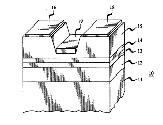
25 profile is critical to optimum device performance. FIG. 1 shows a diagram of a
selectively doped hetreostructure transistor (SDHT) (an FET type device) where
precise doping profile is of importance. The transistor structure 10 is made up of a
substrate 11 made of gallium arsenide and successive layers of AIxGal_xAs. The
aluminum gallium arsenide typically contain from 10 to 40 mole percent aluminum
30 (25 to 35 preferred) and the successive layers are made up of a first layer 12 without
doping, a next layer 13 with doping and a top layer 14 without doping. The firstIayer 12 is a buffer layer, without doping and may vary over large limits in thickness
but usually has a thickness of 1000 to 2000 Angstroms. The next layer 13 (calledhere the doped layer) is doped n-type, typically with silicon or tin in the ~ ~concentration range from 1017 to 102 carriers per cubic centimeters and has a . .
thickness typically from 2 to 400 Angstroms. Preferred are doped layer thicknesses
201 8976
-6-
between 2 and 100 or 2 and 50 or 2 and 20 Angstroms depending on various factorssuch as device application. The top layer 14 is undoped and generally quite thin (e.g.,
10 to 200 Angstroms). On top of this top layer 14 is a layer of gallium arsenide 15
~e.g. 200 to 500 Angstroms thick) with source electrode 16, gate electrode 17 and drain
S electrode 18. A portion of the gallium arsenide layer 15 near the aluminum gallium
arsenide layer 14 is undoped but a 20 to 200 Angstroms thick portion of layer 15 close
to the source 16 and drain 17 is doped n-type to facilitate good ohmic contact. This
structure may be part of the array of similar structures or may be integrated with other
structures on the same semiconductor chip.
An important aspect of this structure is the doped layer 13. This layer
has a high doping concentration with a very sharp doping profile, often with doping ~-
profile half widths less than 50 or even 20 Angstroms. This is highly advantageous
since dopant ions that migrate into the undoped portion of the gallium arsenide layer ~ ;
15 become scattering centers and reduce electron mobility. This structure is
conveniently made by illumination of the growth surface so as to reduce or eliminate
segregation effects that cause redistribution of dopant ions during semiconductor layer
grovth. Other procedures to reduce or eliminate effects of segregation may be used ~ ~ m
including background doping, low growth temperature and use of a crystallographic -
growth surface where Fermi-level pinning does not occur.
FIG. 2 shows a diagram of a selectively doped quantum well structure
_ wjth a gallium arsenide substrate 31, an undoped layer of aluminum gallium
arsenide 32, a doped layer of aluminum gallium arsenide 33 and another undoped layer
oE aluminium gallium arsenide 34. Typically, the aluminum content of the aluminum -
gallium arsenide may vary between 10 and 40 mole percent with 25 to 35 mole percent
preferred. The doped layer 33 is doped with either silicon or tin in carrier
concentrations typically between 10" and 10~ per cubic centimeter. Typically, the first ~ - ;
undoped layer 32 of aluminum gallium arsenide has thickness of about 1000 to 2000
Angstroms, the doped layer 33 between 2 and 400 Angstroms with 2 to 50 or 2 to 20 ~;
preferred and the top undoped layer 34 with thickness between 10 and 200 Angstroms. ~ -;,
On the top of the undoped aluminum gallium arsenide layer 34 is the channel layer 35
made of undoped gallium arsenide, a thin layer 36 of undoped aluminum gallium `
arsenide, then a doped (n-type) layer of aluminum gallium arsenide 37. This layer 31 `
is doped as the doped layer 33. Next is a doped gallium arsenide layer 38, dopedtypically with silicon in the concentration range of 1018 to 10~ per cubic centimeter to
facilitate fabrication of ohmic contacts at the drain 39, Source 40 and gate 41. In
order to obtain devices with superior electronic
20~897~ :
-7- ~ ;
properties, it is critical to have a sharp doping profile so a minimum of the dopant
ions migrate into the channel region 35 where they would create scattering centers
and degrade the mobility of the electrons in the channel region. -These devices are typically made by illuminating the growth surfaces so
5 as to reduce or eliminate migration of the dopant ions and produce extremely sharp
doping profiles. Reduced growth temperature as well as growth on a crystal planesurface where there is no Fermi-level pinning may also be used to produce these
sharp doping profiles. Also useful is background doping to prevent segregation
effects or a combination of these procedures.
FIG. 3 shows a diagram of a heterobipolar transistor 50 made in
accordance with the invention. The device is made up of a collector 51, which is -~
either part of a gallium arsenide substrate or epitaxial layer of gallium arsenide on
top of a substrate. The collector 51 is doped n-type typically with silicon to aconcentration of 10l7 to 10l8 carriers per cubic centimeters. On top of the collector
15 51 is the base 52, made of gallium arsenide and doped p-type typically with
beryllium or carbon as high a concentration as possible but typically in the 10l9 to
102l/cubic centimeter range. On top of the base 52 is the emitter 53, made of ;
aluminum gallium arsenide and doped n-type typically with silicon in the ~ ;
concentration range from lol7 to 10l9 ions per cubic centimeter. Sharp doping
20 profiles are critical to optimum operation of the device.
Other substances may also be used to make these devices including, for
example, indium phosphide and indium ga11ium arsenide, etc.
~,:, ~, . . . : . , : ,, ,. . : ,., : . , : : ., : : . .