Note: Descriptions are shown in the official language in which they were submitted.
^ 1 20 6
., _
Method and Apparatus for Validatin~ a PaPer-like
Piece
This invention re~ates to an apparatus for
validating a paper-like piece such as a bill or bank
note, a note used as a substitute for money, a gift
card, or a bill made of plastics and a collation method
in such apparatus and, more particularly, to such
apparatus and method capable of performing accurate
validation and collation taking into account errors
present in individual parts of an optical sensor or in
assembling of these parts.
In this specification, the term "a paper-like
piece" means a paper-like piece having a face value or
identifying function such as a bill or bank note made of
paper or plastics, a note used as a substitute for
money, a gift card or an identification certificate.
As a sensor used in known validators, there is an
optical sensor including a light-emitting element and a
light-receiving element. In this type of optical
sensor, a bill is passed, for example, between the
light-emitting element and the light-receiving element
and the amount of transmitted light corresponding to the
design on the bill is detected, and the pattern on the
bill is collated on the basis of the detected amount of
2019165
, -2-
_
transmitted light to validate the bill. There is also
proposed a method of detecting the amount of reflected
light in accordance with the pattern on the bill. As
examples of such prior art optical type bill validator
or bill validating method, there are publications
including Japanese Patent Publication No. 41-20245,
Japanese Utility Model Publication No. 43-23522,
Japanese Patent Publication No. 53-39151, Japanese
Patent Application Laid-open No. 54-5496 and Japanese
Patent Application Laid-open No.60-61883.
Japanese Patent Publication No. 41-20245 and
Utility Model Publication No. 43-23522 disclose a
general art of validating a bill by comparing a received
light signal corresponding to the pattern of the bill
with a predetermined reference pattern. Japanese Patent
Publication No. 53-39151, Patent Application Laid-open
No. 54-5496, Patent Application Laid-open No. 60-61883
and others disclose a technique for coping with
variation in the received light level occurring due to
variations in the measuring conditions which are
resultant from aging and thermal property of the light-
emitting and light-receiving elements and deposition of
soil on a bill.
A typical example of the prior art for coping with
variation in the received light level due to variations
in measuring conditions is a method according to which
3 2019165
the received light signal level in a stand-by mode
(i.e., a mode in which a bill has not been inserted in
the validator) is measured, and then a pattern of a bill
is normalized on the basis of the measured value. In
other words, reference pattern data is prepared in the
form of a ratio of a received light signal level
corresponding to a detected pattern, to a received light
signal level in the stand-by mode. The received light
signal level in the stand-by mode (current stand-by mode
level) is measured at each occasion of detection, then a
received light signal level corresponding to the pattern
of an inserted bill which is measured at each occasion
of detection is converted to the ratio to the current
stand-by mode level and this ratio is compared with the
reference pattern data. In short, the received light
signal level which is an absolute value is converted to
a relative value based on the stand-by mode for
collation.
In the above described prior art method, no serious
problem arises in cases where a high degree of accuracy
of validation is not required. In a case where a high
degree of accuracy of validation is required, however,
the following problem will arise. In a case, for
example, where a magnetic validation device performing
validation by detecting a magnetic component in printing
ink is provided in addition to the optical type
2019i6~
4--
validation device for improving the accuracy of
validation, the accuracy of validation by the optical
validation device per se may be relatively rough. In a
case where no magnetic component exists in the printing
ink, however, there is no means for improving the
accuracy of validation but performing an accurate
validation with the use of the optical type validation
device and, accordingly, a high degree of accuracy of
validation by the optical type validation device per se
is required.
A problem caused by the optical type validation
device is a problem caused by a parts error and an
assembling error of the optical sensor. The parts error
is an error in individual elements such as a light-
emitting element and a light-receiving element which are
used as parts of an optical sensor. Even if each part
is made so as to satisfy a certain standard, there is an
irregularity between individual elements within the
standard. Accordingly, the amount of emitted light may
differ from element to element even if the same input
electrical signal is given, or output electrical signals
may differ even if the same amount of light is received,
or the irradiation field pattern of the light-emitting
element may differ from element to element. This is the
parts error. The assembling error is an irregularity in
the accuracy of assembling of parts of an optical
2 0 1 9 1 6 5
--5--
_
sensor, that is, the relation between the irradiation
field of the light-emitting element and the position of
the light-receiving element differs slightly from one
optical sensor to another due to irregularity in
assembling of the parts.
Figs. 12a - 12c show, as an example of the parts
error, irregularities between the irradiation field
patterns of individual light-emitting elements. Fig.
12a shows an example in which a half-bright spot is
located in the center of a bright circle. Fig. 12b
shows an example in which a half-bright spot is located
in the center of a bright circle and further a bright
spot is located in the center of the half-bright spot.
Fig. 12c shows an example in which a half-bright spot is
located at a position slightly offset from the center of
a bright circle.
Figs. 13a and 13b show, as an example of the
assembling error, irregularities in the locational
relations between irradiation fields Ll and L2 of a
light-emitting element and position R of a light-
receiving element. Ll denotes a bright circle and L2 a
half-bright spot. Fig. 13c shows an example in which
there is substantially no assembling error with respect
to irradiation field Ll, but position R of a light-
receiving element with respect to irradiation fields Ll
and L2 is offset due to offsetting of the irradiation
-- - 2019165
_
field L2 with respect to the irradiation field Ll.
Such parts and assembling errors adversely affect
the output signal level of a light-receiving element.
This effect is relatively small when received light is
in a saturated or nearly saturated state but becomes
remarkable in a moderate light receiving state
corresponding to the pattern on a bill.
Fig. 14 shows an example of a light-receiving
element's output signal in a light transmitting system.
In the stand-by mode, the received light is in a
saturated state and the light-receiving element's output
signal level is at the maximum. When a bill is passing
through an optical sensor, light is interrupted and the
light-receiving element output signal level therefore
drops and there arises variation in the light-receiving
element's output signal level corresponding to the
pattern of the bill. By comparing and collating the
variation pattern of this light-receiving element's
output signal level during passing of the bill with a
predetermined reference pattern, the inserted bill is
validated. In the figure, solid line X shows an example
of a ligth-receiving element's output signal of a
certain appratus and dotted line Y shows an example of a
light-receiving element output signal of another
apparatus concerning the same bill. The light-receiving
element output signal level differs depending upon the
--7--
parts error and assembling error in an optical sensor in
each apparatus. For example, the light-receiving
element output signal level in the stand-by mode is TlOW
in the solid line X whereas it is T20W in the dotted
line Y. The light-receiving element's output signal
level during passing of the bill also differs between
the solid line X and the dotted line Y. For example, at
a point A, the signal level is TlOa in the solid line X
but it is T20a in the dotted line Y.
The ratio of the light-receiving element's output
signal level during passing of the bill to the light-
receiving element's output signal level in the stand-by
mode at the point A is TlOa/TlOW in the solid line X and
T20a/T20W in the dotted line Y. Owing to difference
between T10W and T20W and difference between TlOa and
T20a, values of the respective ratios are different from
each other. If, therefore, common reference pattern
data is used, there arises the problem that an accurate
validation cannot be performed.
Even if the value of reference pattern data is
changed for each apparatus, the conventional normalizing
method of obtaining a ratio of the light-receiving
element's output signal level during passing of the bill
to the light-receiving element's output signal level in
the stand-by mode has the problem that the parts and
assembling errors affect the accuracy adversely, because
- - ~ 2019165
--8--
one of the output signal levels is a saturated value and
the other is an unsaturated value so that difference
between the two values is large, thus with a resulting
small value of ratio making it difficult to perform an
accurate validation, and, further because the effect of
the parts and assembling errors is relatively small in
the saturated value whereas this effect is remarkable in
the unsaturated value. Further, aging due to soil or
deterioration of the sensor affects the difference or
ratio between the saturated value and the unsaturated
value caused by the parts and assembling errors, which
becomes one of the reasons for inability of the
conventional method to improve the accuracy in
validation.
It is, therefore, an object of the invention to
provide a method and an apparatus for validating a
paper-like piece capable of performing accurate
validation and collation taking into account the parts
and assembling errors of an optical sensor.
It is another object of the invention to provide a
method and an apparatus for validating a paper-like
piece capable of performing accurate val idation and
collation taking into account the parts and assembling
errors regardless of variation in the measuring data due
- -9- ~01916~
to soil or fatigue of a paper-like piece or soil or
deterioration of the sensor.
The apparatus for validating a paper-like piece
according to the invention comprises a detection
section for producing a detection signal corresponding
to a pattern onto a deposited paper-like piece by
irradiating light on the paper-like piece, a reference
level data providing section for preparing reference
level data on the basis of a detection signal produced
by said detection section in response to deposition of a
reference paper-like piece on which no particular
pattern is provided and providing this reference level
data, a standard pattern providing section for providing
a predetermined standard pattern corresponding to a
pattern of a true paper-like piece, a data-to-be-
examined providing section for providing data to be
examined which is obtained by converting a detection
signal produced by said detection section in response to
depositin of a paper-like piece to be validated to a
ratio to or deviation from the reference level data
provided by said reference level data providing section,
and a determination section for determining whether the
paper-like piece to be validated is true or false by
collating the data to be examined provided by said data-
to-be examined providing section with the standard
pattern provided by said standard pattern providing
- ^ 2 0 1 9 1 6 5
--10--
._
section.
According to the invention, reference level data
for normalization is provided by using a reference
paper-like piece having no particular pattern (e.g., a
white paper). For this purpose, the reference level
data providing section is provided. For providing the
reference level data by this reference level data
providing section, the reference paper-like piece is
deposited and, on the basis of the detection signal
produced by the detection section in response to this
deposition, the reference level data is obtained.
The standard pattern providing section provides a
predetermined standard pattern corresponding to a
pattern of a true paper-like piece. This standard
pattern is provided not in an absolute value level but
in the form of a ratio to or a deviation from the
reference level data. The standard pattern may either
be one which is established individually for each
apparatus or one which is common to all apparatuses.
The data-to-be-examined providing section provides
data to be examined by converting a detection signal
produced by the detection section in response to
deposition of a paper-like piece to a ratio to or
deviation from the reference level data. The
determination section determines whether the deposited
paper-like piece is true or false by collating the data
2019165
to be examined provided by the data-to-be-examined
providing section with the standard pattern provided by
the standard pattern providing section.
Since the base for normalizing measured data for
collation is not set at a saturation level but set at
the level of the reference paper-like piece, validation
becomes less vulnerable to adverse effects by the parts
and assembling errors in an optical sensor whereby the
validation accuracy can be improved.
Besides, since the validation is less vulnerable to
adverse effects by the parts and assembling errors of
the optical sensor, there is the advantage that the
validation accuracy can be improved in a case where
common standard pattern data is used for all
apparatuses.
In one aspect of the invention, the apparatus for
validating a paper-like piece comprises, in addition to
the above described elements, a paper-like piece absence
level data providing section for providing paper-like
piece absence level data in response to the output
signal of said detection section produced when a paper-
like piece is not deposited, and a reference level data
correction section for correcting the reference level
data in accordance with difference between initial
paper-like piece absence level data which has been
provided by said paper-like piece absence level data
- - 201916~
-12-
_. .
providing section during the same period of time as the
reference level data has been obtained and current
paper-like piece absence level data which has currently
been provided by said paper-like piece absence level
data providing section.
By providing the paper-like piece absence level
data providing section and the reference level data
correction section, errors caused by temperature change,
aging of the sensor, or deposition of soil or dust on
the sensor can be successfully eliminated or reduced.
The collation method in a paper-like piece
validating apparatus according to the invention
comprises a first step in which a reference paper-like
piece having no particular pattern is deposited and
reference ievel data is provided on the basis of
detection signal produced by a detection section in
response to this deposition, a second step in which a
predetermined standard pattern corresponding to a
pattern of a normal paper-like piece is provided, a
third step in which a detection signal produced by the
detection section in response to deposition of a paper-
like piece to be validated is converted to a ratio to or
deviation from the reference level data and this ratio
or deviation is provided as data to be examined, and a
fourth step in which the data to be examined is collatedwith the standard pattern to determine whether the
-~ ~13 201916~
deposited paper-like piece is true or false.
Embodiments of the invention will now be described
with reference to the accompanying drawings.
In the accompanying drawings,
Figs. 1 and 2 are block diagrams showing a
functional construction of an embodiment of the
apparatus for validating a paper-like piece according to
the invention;
Fig. 3 is a graph showing an example of simulation
of a bill detection signal for explaining effects of the
parts error and assembling error in an optical type
detector in each apparatus;
Fig. 4 is a graph showing an example of simulation
of a bill detection signal for explaining effects of the
output error in an optical type detector caused by
environmental change or aging in one and the same
apparatus;
Fig. 5 is a side view showing schematicallY a
mechanical portion in the embodiment of the paper-like
piece validating apparatus incorporating the invention;
Fig. 6 is a block diagram showing an example of an
electrical hardware circuit in a control section of the
same embodiment;
Figs. 7 through 9 are flow charts showing an
example of a program executed by a mircocomputer section
~- 2019165
-14-
in Fig. 6;
Figs. 10 and 11 are flow charts showing another
example of a program executed by the microcomputer
section in Fig. 6;
Figs. 12a - 12c are diagrams showing irregularity
in the irradiation field of respective light-emitting
elements for illustrating an example of the parts error;
Figs. 13a - 13c are diagrams showing irregularity
in the relation between the irradiation field of
respective light-emitting elements and the position of
light-receiving elements; and
Fig. 14 is a diagram showing an example of an
output from a light-receiving element in the light
transmission measuring system.
- 2019165
-15-
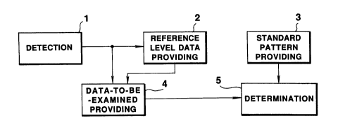
Referring to Fig. 1, reference numeral 1 represents
a detection section, 2 a reference level data providing
section, 3 a standard pattern providing section, 4 a
data-to-be-examined providing section and 5 a
determination section, respectively. The reference level
data for normalization is provided by using a reference
paper-like piece having no particular pattern (e.g.,
white paper). For this purpose, the reference level
data providing section 2 is provided. For providing the
reference level data by this reference level data
providing section 2, a reference paper-like piece is
deposited and reference level data is obtained on the
basis of a detection signal produced by the detection
section 1 in response to this deposition.
In a case where the light transmission system is
employed, the level of received light in the detection
section 1 upon deposition of a reference paper-like
piece is lower than a saturation level and is in the
vicinity of the level of received light UPon deposition
of a paper-like piece to be examined. Fig. 3 shows an
example of reference levels TlOP and T20P corresponding
to the reference paper-like piece. TlOP is an example
of reference level corresponding to a paper-like piece
which has been detected by an optical type detection
section set in a certain apparatus. An example of a
- 201916~
-16-
-
pattern of the paper-like piece which has been detected
by this detection section is shown by the solid line X.
T20P is an example of reference level corresponding to
the same reference paper-like piece which has been
detected by an optical type detection section set in
another apparatus. An example of a pattern of a paper-
like piece which has been detected by this detection
section is shown by the dotted line Y. In the same
manner as in Fig. 14, TlOW and T20W are examples of
output signal levels of the optical type detection
sections in the stand-by mode (i.e., saturation levels)
and TlOa and T20a are examples of output signal levels
of the optical type detection sections at a point A of
the paper-like piece to be examined.
The standard pattern providing section 3 provides a
predetermined standard pattern corresponding to a
pattern of a paper-like piece to be examined. This
standard pattern is provided not as an absolute value
level but as a ratio to or deviation from the reference
level data. Assuming, for example, that a standard
received light signal level value of a paper-like piece
to be examined at the point A is represented by TlOa'
and the reference level is represented by TlOp', the
value of the standard pattern corresponding to the point
A is provided in the form of a ratio TlOa'JTlOp'. This
value may also be provided in the form of a deviation
~ 201916~
-17-
TlOp' - TlOa'. The standard pattern to be provided in
this manner may be a different pattern for each
apparatus or may be a common pattern for all
apparatuses.
The data-to-be-examined providing section 4
converts a detection sigal produced by the detection
section 1 in response to depositon of a paper-like piece
to a ratio to or deviation from the reference level data
and provides this ratio or deviation as data to be
examined. For example, as to a received light signal
level value TlOa of a paper-like piece at the point A in
the first described apparatus in the foregoing example,
data to be examined is provided in the form of a ratio
TlOa/TlOp or a deviation TlOp - TlOa with respect to
the reference level TlOp. As to a received light signal
level value T20a in the other apparatus in the foregoing
example, data to be examined is provided in the form of
a ratio T20a/T20p or a deviation T20p - T20a with
respect to the reference level T20p.
The determination section 5 determines whether the
deposited paper-like piece is true or false by collating
the data to be examined provided by the data-to-be-
examined providing section 4 with the standard pattern
provided by the standard pattern providing section 3.
Assuming, for example, that a certain common standard
pattern is used by the two different apparatuses in the
2019165
-18-
-
foregoing example, the value of the standard pattern is
TlOa'/TlOp' with respect to the point A. If a measured
value of the point A of a deposited paper-like piece in
the first described apparatus, i.e., data to be
examined, is TlOa/TlOp, these two values are compared
and collated with each other. Likewise, if a measured
value of the point A of a deposited paper-like piece in
the other apparatus is T20a/T20p, this value is compared
and collated with the standard pattern value TlOa'/TlOp'
at the point A.
Since, as described above, the base for normalizing
the measured data for collation is not set at a
saturation level (e.g., TlOW or T20W) but set at the
level of the reference paper-like piece (e.g., TlOp or
T20p), validation becomes less vulnerable to adverse
effects by the parts and assembling errors in an optical
sensor used as the detection section 1 whereby the
validation accuracy is improved.
Besides, since the validation is less vulnerable to
adverse effects by the parts and assembling errors which
are peculiar to the optical sensor in each apparatus,
the validation accuracy can be improved in a case where
common standard pattern data is used for all
apparatuses.
The embodiment of Fig. 2 comprises, in addition to
the above described elements, a paper-like piece absence
~ 201916~
--19--
-
level data providing section 6 for providing paper-like
piece absence level data in response to the output
signal of said detection section produced when a paper-
like piece is not deposited, and a reference level data
correction section 7 for correcting the reference level
data in accordance with difference between initial
paper-like piece absence level data which has been
provided by said paper-like piece absence level data
providing section 6 during the same period of time as
the reference level data has been obtained and current
paper-like piece absence level data which has currently
been provided by said paper-like piece absence level
data providing section 6.
By providing the paper-like piece absence level
data providing section 6 and the reference level data
correction section 7 as shown in Fig. 2, errors caused
by temperature change, aging of the sensor, or
deposition of soil or dust on the sensor can be
successfully eliminated or reduced.
An example of correction of reference level data is
shown in Fig. 4 in which intial paper-like piece absence
level data is represented by TlOW and current paper-like
piece absence level data reflecting the environmental
change and aging is represented by TllW. An example of
initial data of a pattern of a paper-like piece to be
examined which has been detected by an optical type
2 0 1 9 1 6 5
-20-
detection section set in a certain apparatus is shown by
a solid line X10 and an example of data reflecting the
environmental change and aging in the pattern of the
paper-like piece to be examined which has been detected
by the optical type detection section in the same
apparatus is shown by a dotted line X11. Paper-like
piece absence level data in the solid ! ine X10 is
represented by TlOW and paper-like piece absence level
data in the dotted line X11 is represented by TllW.
Reference level data is represented by TlOp.
By way of example of correction by the reference
level data correction section 7 in accordance with
difference between the current paper-like piece absence
level data TllW and the initial paper-like piece absence
level data TlOW, the reference level data T1Op can be
corrected by a ratio of the current paper-like piece
absence level data TllW to the initial paper-like piece
absence level data TlOW. That is, a correction TlOp x
TllW/TlOW = Tllp is performed. Tllp represents
reference level data after correction. If the current
paper-like piece absence level data T11W is not
different from the initial paper-like piece absence
level data TlOW, TlOp = Tllp, i.e., the reference level
data TlOp does not change. Thus, the reference level
data is corrected in accordance with change of the
current paper-like piece absence level data TllW
`~ 2019165
-21-
relative to the initial paper-like piece absence level
data TlOW whereby the errors in the optical type
detection section due to the environmental change and
aging can be successfully coped with.
Fig. 5 is a side view showing a mechanical section
of the embodiment of the paper-like validation apparatus
according to the invention. In this embodiment, the
validation apparatus handles a bill or bank note as the
paper-like piece. In the vicinity of an insertion slot
is disposed an optical sensor 11 for detecting insertion
of a bill. Upon insertion of the bill, the bill is
detected by the optical sensor 11 and a motor 18 is
driven in a forward direction in response thereto to
actuate belts 19 and 20 stretched between pulleys 14, 15
and 16, 17. As the belts 19 and 20 are actuated, the
bill held between the belts 19 and 20 is conveyed into
the apparatus. In the apparatus, there are provided one
or more optical sensors for detecting characteristic
features of the bill. In this embodiment, there are
provided two optical sensors 12 and 13. These optical
sensors 12 and 13 are arranged in different positions in
the bill conveying direction so as to detect respective
characterizing features of the bill at different
positions over the bill. Each of the optical sensors
11, 12 and 13 consists of a pair of a light-emitting
element and a light-receivig element and the bill is
-- -22- 201 16~
caused to pass between these light-emitting element and
light-receiving element for detection of the amount of
transmitted light by the light-receiving element.
Fig. 6 shows an example of an electrical hardware
circuit of a control section provided in association
with the mechanical section of Fig. 5. This control
section has a microcomputer including a CPU (central
processing unit) 21, a program ROM 22 and a data and
working RAM 23 and executes various processings under
the control by this microcomputer. The output of the
optical sensor 11 detecting insertion of the bill is
supplied to a waveform rectifying circuit 24 which
produces a signal "1" or "0" in response to presence or
absence of a bill. This signal is applied to the CPU
21. Output signals of the optical sensors 12 and 13 for
detecting the characterizing features of the bill are
supplied to amplifying circuits 25 and 26 and, after
amplification, are applied to channels CH1 and CH2 of an
analog-to-digital converter 27, respectively. The
analog-to-digital converter 27 converts the output
analog signal of the optical sensors 12 and 13 applied
to the channels cHl and CH2 to digital data by a time
division processing and supplies the converted digital
signals to the CPU 21.
To the rotation shaft of the drive motor 18 is
attached a rotary encoder 28 which generates incremental
2019165
-23-
pulses or absolute angle detection value data in
response to rotation of the motor 18. The output of
this rotary encoder 28 is supplied to the CPU 21.
A standard pattern memory 29 stores standard
pattern data corresponding to the pattern of a true
bill. The standard pattern memory 29 stores standard
pattern data in correspondence to the respective
characterizing feature detection optical sensors 12 and
13. By way of example, it is assumed that the standard
pattern data stored in this standard pattern memory 29
is transmitted light level data which has not been
normalized.
- A writable read-only memory (ROM) 30 consisting,
for example, of an EPROM stores reference level data or
data obtained by correcting this reference level data by
initial paper-like piece absence level data for each
apparatus. As a first example, reference level data
itself is stored in this RPROM 30.
Description will first be made about a case where
measures are taken for coping with the parts and
assembling errors without taking the environmental
change and aging into consideration. In this case,
reference level data itself is stored in the EPROM 30.
An example of processings executed in the CPU 21 in this
case is shown in the flow charts of Figs. 7 through 9.
Writing of the reference level data into the EPROM
. - 2019165
-24-
30 is made by processings shown in Fig. 7. The
processings of Fig. 7 are executed in the final stage of
manufacturing and assembling of each bill validating
apparatus.
First, a mode in which a reference paper having no
particular pattern is deposited is established. Upon
deposition of the reference paper, each reference level
data is measured by the characterizing feature detecion
optical sensors 12 and 13. The measured reference level
data are represented by reference characters TlOp. The
respective reference level data TlOp measured by the
optical sensors 12 and 13 are written and stored in the
EPROM 30. Since the optical property of reference paper
is uniform at any surface position thereof, reference
level data TlOp may be obtained representatively by
either one of the optical sensors 12 and 13 instead of
obtaining reference level data TlOp by both of the
optical sensors 12 and 13 and this single reference
level data TlOp may be stored in the EPROM 30 and used
as reference level data TlOp which is common to the
optical sensors 12 and 13.
Next, processings during operation of the bill
validating apparatus will be described with reference to
the flow charts of Figs. 8 and 9.
Upon turning on of a power source, the processings
of Fig. 8 are executed. Reference level data TlOp
201916S
-25-
-
corresponding to the characterizing feature detection
optical sensors 12 and 13 are read from the EPROM 30 and
standard pattern data corresponding to the optical
sensors 12 and 13 are read from the data memory 29.
Then, an operation for normalizing the standard
pattern data with the use of the reference level data
TlOp is performed for each of the characterizing feature
detection optical sensors 12 and 13. Representing
standard pattern data corresponding to each sample point
of the bill by Tx (where x represents each sample point
of the bill and, if the bill contains n sample points, x
= 1, 2, ......... n), an operation Tx/TlOp is performed
with respect to each x. In other words, TxJTlOp is a
ratio of the standard pattern data Tx corresponding to
each sample point x to the reference level data TlOp
which is 100%.
Thereafter, the standard pattern data Tx/TlOp which
has been converted to the ratio to the reference level
data TlOp is stored in the RAM 23. These normalized
standard pattern data Tx/TlOp are stored in the RAM 23
in correspondence to the respective optical sensors 12
and 13. By this.normalizing operation, the standard
pattern data Tx/TlOp which has been converted to the
ratio to the reference level data TlOp can be provided
by reading it from the RAM 23.
Upon deposition of a bill, processings of Fig. 9
- ~ 201916S
-26-
,
are executed. First, detection signals produced by the
characterizing feature detection optical sensors 12 and
13 are sampled and stored in predetermined areas in the
RAM 23 as required. The level of the detection signal
at a certain measuring sampling point A is represented
by TlOa.
Reference level data TlOp corresponding to the
characterizing feature detection sensors 12 and 13 are
respectively read from the EPROM 30 and an operation
"TlOa/TlOp" for converting the detection signal levels
TlOa corresponding to the respective optical sensors 12
and 13 to a ratio to the reference level data TlOp is
performed. In other words, TlOa/TlOp is the ratio of
the detection signal level TlOa to the reference level
data TlOp which is 100~. The operation result TlOa/TlOp
is stored in the RAM 23 as required. In this manner,
data "TlOa/TlOp" which is the detection signal level
TlOa converted to its ratio to the reference level data
TlOp is provided as data to be examined.
Thereafter, the standard pattern data Tx/TlOp
stored in the RAM 23 by the processings of Fig. 8 is
read out and the data to be examined "TlOa/TlOp" which
has been obtained in the above described manner is
collated with this standard pattern data Tx/TlOp. This
collation is made with respect to each measuring sample
point in correspondence to the respective characterizing
,- ' ;'Q 2019165
-27-
feature detection optical sensors 12 and 13 and
determination as to whether the deposited bill is true
or false is made on the basis of results of the
collation.
In a modification of the above described
embodiment, previously normalized data Tx/TlOp may be
prestored in the manufacturing process in a factory as
standard pattern data stored in the data memory 29. In
this case, the processings of Fig. 8 are omitted. In
the above described embodiment in which the normalized
standard pattern data Tx/TlOp is obtained by the
processings of Fig. 8, TlOp differs one apparatus from
another so that the standard pattern data Tx/TlOp has a
value peculiar to each apparatus. In a case where the
standard pattern data Tx/TlOp which has been normalized
in the manufacturing process in the factory is stored as
in the modified example, the common standard pattern
data Tx/TlOp is used in all apparatuses. Even in this
case, the operation of the data to be examined TlOa/TlOp
of Fig. 9 is performed for each apparatus in accordance
with the reference level data TlOp peculiar to each
apparatus. Accordingly, the advantage of the present
invention can be enjoyed in this case also.
Description will now be made about a case where
measures are taken for coping with the environmental
change and aging as well as the parts and assembling
- ~ 20191~
-28-
.
errors of the optical sensors. In this case, for coping
with the environmental change and aging, paper-like
piece absence level data which is an output of each of
the characterizing feature detection optical sensors 12
and 13 produced when a bill is not deposited is measured
and utilized for the control. For example, the EPROM 30
stores reference level correction data obtained by
correcting reference level data by initial paper-like
piece absence level data. An example of processings by
the CPU 21 in this case is shown in flow charts of Figs.
10 and 11.
Fig. 10 shows, as Fig. 7, writing of reference
level data in the EPROM 30. This processing is made in
the final stage of manufacturing and assembling of each
bill validating apparatus.
In Fig. 10, as in Fig. 7, a reference paper having
no particular pattern is deposited and reference level
data TlOp is measured. The processing of Fig. 10 is
different from that of Fig. 7 in that the paper-like
piece absence level data is measured on the basis of
outputs of the characterizing feature detection optical
sensors 12 and 13 produced when a bill is not deposited.
The paper-like piece absence level data is obtained
during the same period of time as the reference level
data TlOp is obtained. That is, the outputs of the
characterizing feature detection optical sensors 12 and
~- 201gl6~
-29-
-
13 are loaded as paper-like piece absence level data
immediately before deposition of a reference paper or
immediately after removal of a reference paper and are
provided as initial paper-like piece absence level data
TIOW. The ratio TlOp/TlOW of the reference level data
TlOp to the initial paper-like piece absence level data
TlOW is then obtained and this ratio is written ans
stored in the EPROM 30. This reference level correction
data TlOp~TlOW is obtained for each of the
characterizing feature detection optical sensors 12 and
13 and stored in the EPROM 30.
Referring to Fig. 11, processings executed when the
bill validating apparatus in in operation will be
described.
Upon turning on of the power source, processings of
Fig. 11 are executed. In the processings of Fig. 11,
the output of the deposition detection optical sensor 11
is examined and, if it is in a state where a bill is not
detected, i.e., the stand-by mode, outputs of the
characterizing feature detection sensors 12 and 13 are
loaded and stored in the RAM 23 as current paper-like
piece absence level data (represented by TllW).
Then, reference level correction data TlOp/TlOW
corresponding to the characterizing feature detection
optical sensors 12 and 13 are read from the EPROM 30 and
operated with the current paper-like piece absence level
201916~
-30-
-
data TllW corresponding to the optical sensors 12 and 13
to provide reference level data (represented by Tllp)
obtained by correcting reference level data by a ratio
TllW/TlOW of the current paper-like piece absence level
data TllW to the initial paper-like piece absence level
data TlOW. The ratio TllW/TlOW of the current paper-
like piece absence level data TllW to the initianl
paper-like piece absence level data TlOW corresponds to
an output error of the optical sensor caused by the
environmental change and aging. The reference level data
TlOp obtained at the time of assembling the apparatus is
adjusted in accordance with this output error of the
optical sensor caused by the environmental error and
aging. The operation is made by multiplying the
reference level correction data TlOp/TlOW with the
current paper-like piece absence level data TllW. By
this operation, Tllp = TllW x TlOp/TlOw is obtained.
This is Tllp = TlOp x TllW/TlOW which is the product of
the ratio TllW/TlOW of the current paper-like piece
absence level data TllW to the initial paper-like piece
absence level data TlOW and the reference level data
TlOp, and is obtained by correcting the reference level
data TlOp in accordance with the ratio TllW/TlOW. In a
case, for example, where there is no output error of the
optical sensor caused by the environmental change and
aging, TllW = TlOW so that Tllp = TllW x TlOp/TlOW
- ~` 2019165
-31-
-
TlOp and hence the reference level data TlOp is not
corrected. If TllW is not equal to TlOW, the initial
reference level TlOp is corrected in accordance with
difference between TllW and TlOW and this constitutes
the corrected reference level data Tllp. This corrected
reference level data Tllp is stored in the RAM 23.
Then, standard pattern data Tx corresponding to the
characterizing feature detection optical sensors 12 and
13 are respectively read from the data memory 29 and the
operation for normalizing the standard pattern data Tx
with the use of the corrected reference level data Tllp
is made for the respective characterizing feature
optical sensors 12 and 13. This operation consists of
an operation Tx/Tllp for each sample point x (where x
1, 2, 3, ......... n) in the same manner as the operation
shown in Fig. 8. That is, Tx/Tllp is the standard
pattern data Tx for each sample point x which has been
converted to its ratio to the corrected reference level
data Tllp which is 100%.
Thereafter, the standard pattern data Tx/Tllp which
has been converted to its ratio to the corrected
reference level data Tllp is stored in the RAM 23.
The normalized standard pattern data Tx/Tllp
corresponding to the optical sensors 12 and 13 are
stored in the RAM 23. The standard pattern data Tx/Tllp
which has been converted to the ratio to the corrected
~ 2019165
-32-
-
reference level data Tllp by the normalizing operation
is provided by reading it from the RAM 23.
Upon deposition of a bill, presence of the bill is
detected in the step of output detection in the optical
sensor 11 In Fig. 11 and, as in Fig. 9, the outputs of
the characterizing feature detection optical sensors 12
and 13 are collated with the standard pattern data
Tx/Tllp of the RAM 23.
Detection signals produced by the characterizing
feature detection optical sensors 12 and 13 are sampled
and stored in predetermined areas in the RAM 23 as
required. The level of the detection signals at a
certain measuring sample point A is represented by Tlla.
Then, the corrected reference level data Tllp
corresponding to the respective characterizing feature
detection optical sensors 12 and 13 are read from the
RAM 23 and an operation "Tlla/Tllp" for converting the
detection signal levels Tlla corresponding to the
respective optical sensors 12 and 13 to ratios to the
corrected reference level data Tllp is performed.
Tlla/Tllp is the detection signal Tlla converted to its
ratio to the corrected reference level data Tllp which
is 100%. The results of operation Tlla/Tllp are stored
in the RAM 23 as required. Thus, the data "Tlla/Tllp"
which is the detection signal level Tlla converted to
its ratio to the corrected reference level data Tllp is
~ 2019165
-33-
provided as data to be examined.
Thereafter, the standard pattern data Tx/Tllp
stored in the RAM 23 by the processing in the stand-by
mode is read out and the data to be examined "Tlla/Tllp"
obtained in the above described manner is collated with
the standard pattern data Tx/Tllp. The collation is
made at each measuring sample point with respect to each
of the characterizing feature detection optical sensors
12 and 13 and whether the deposited bill is true or
false is determined in accordance with the results of
collation.
In the embodiment of Figs. 10 and 11 also,
previously normalized data Tx/TlOp may be prestored in
the data memory 29 in the manufacturing process in a
factory as the standard pattern data to be stored in the
data memory 29. In this case, Tx/Tllp can be obtained
by multiplying Tx/TlOp with TlOW/TllW in the processing
in the stand-by mode in Fig. 11.
In the above described embodiments, the reference
level data TlOp or the corrected reference level data
TlOp/TlOW is written and stored in the writable read-
only memory 29. The invention is not limited to this
but, for example, the reference level data TlOp/TlOW
measured during assembling of the apparatus or the
corrected reference level data TlOp/TlOW may be
displayed at a suitable time so that the operator may
~ 2019165
-34-
-
watch this display and set and input the reference level
data TlOp or the corrected reference level data
TlOp~TlOW in a digital or analog value by means of a
digital switch or an analog setting device. In this
case, during the operation of the bill validating
apparatus, a program is made so that set contents of the
digital switch or analog setting device may be referred
to as required thereby to enable the operator to utilize
the reference level data TlOp or the corrected reference
level data TlOp/TlOW.
In the above described embodiments, validation of
a paper-like piece is made by the software processings.
The validation may however be realized by using a
wired hardware logic.
The deposition detection optical sensor 11 and the
characterizing feature detection optical sensors 12 and
13 are not limited to optical sensors of a transmitted
light measuring type but may also be optical sensors of
a reflected light measuring type.
In the above described embodiments, description has
been made about an apparatus which handles a bill or
bank note. The invention however is applicable also to
apparatuses which handle other paper-like pieces having
a pattern corresponding to a certain value such as
a draft like a bank draft, a note used as a substitute
for money, a gift card and a bill made of plastics.
2019165
-35-
As described above, since, according to the
invention, the base for normalizing measured data for
comparison and collation is not set at a saturation
level but set at the level of a reference paper-like
piece, validation becomes less vulnerable to adverse
effects by the parts and assembling errors in an optical
sensor whereby the validation accuracy can be improved.
Further, since the reference level data is corrected in
accordance with difference produced due to the
environmental change and aging between the initial
paper-like piece absence level data and the current
paper-like piece absence level data, errors occurring in
the optical type detection section due to the
environmental change and aging can be eliminated or
reduced.