Note: Descriptions are shown in the official language in which they were submitted.
201 9~78
DIRECT MODULATION PHASE-SHIFT-KEYING SYSTEM AND MET~OD
BACKG~OUND OF THR INVENTION
The present invention relates to a PSK (phase
shift ~eying) system and method in a coherent optical
fiber transmission and more particularly to a PSK system
and method adapted to be able to directly modulate an
injection current supplied to a laser diode.
Of the optical fiber transmission systems in
practical use today, an IM/DD ~intensity
modulation/direct detection) sy~tem in which an
intensity modulated light beam i8 directly received by a
photodetector and converted thereby into an electric
~ignal is quite general. In recent years, however,
research and development for a coherent optical fiber
transmission system has become actively carried on
because of strong demands for larger transmission
capacity and longer transmission distance. According to
thL~ system, since a coherent light beam from 8 laser
diode ls u~ed as the carrier and its frequency, phase,
0tc. are modulated on the transmis~ion side and the
received light beam is mixed with a local light beam 80
a~ to be subjected to heterodyne detection or homodyne
detectton on the receptLon ~ide, a greater improvement
~,
, ~, ',: ,:,''
2 ~ 7 8
in the reception sensitivity compared with the IM/DD
system can be achieved. Further, after the detection of
the light has been performed, i.e., after the light
signal has been converted into an electric signal,
frequency selection can be made rather easily. Hence,
high-density frequency-division multiplexing can be
achieved by this system and the transmission cspRcity by
a single optical transmission path can thereby be
greatly increHsed.
AB a system or method for transmitting
information with the information carried by the wave
parameter of a light beam emitted from a laser diode and
being suitable for high speed transmission, DPSK
(differential phase shift keying) or CPFSK (continuous
phase frequency shift keying) has hitherto been known.
In the DPSK system, in order that a
demodulation by delayed detection by one bit i6
performed on the reception ~ide, differential coding is
made on the transmission side in advance. The
modulation through the differentially coded signal is an
indirect modulation u~ing an external modulator.
In the CPFSK system, on the other hand, the
oscillation frequency of the la~er diode is directly
modulated on the transmission side so that the phase
2 ~ 7 ~
deviation between different signs becomes over ~ with
the phase maintained continuous, and a demodulation with
delayed detection is performed on the reception side.
'rhe delay time is set according to one time slot and the
modulation index.
In the DPSK system, aD external modulator is
required and the loss due to its insertion (for example,
2 to ~ dB) becomes a cause of the deterioration in the
reception sensitivity. Further, since most of the
external modulators are such that utilize the electro-
optic effect of an anisotropic crystal, it requires
driving voltage of several to ten-odd Volts for
obtaining a frequency band of several GHz. Further, a
differential coding circuit i8 required for achieving a
demodulation by delayed detection by one bit. Thus, the
DPSK system become~ complex in structure.
In the CPFSK system, although neither external
modulator nor differential coding circuit is required,
the system is liable to be adversely affected by the
wavelength dispersion and, hence, it~ transmission spar
is limited. Further, the carrier is unable to be
reproduced for use in the CPFSK system.
2019178
28170-8
SUMHARY OF THE INVENTION
An object of the present invention is to provide a PSK
system and method adapted to simplify the system structure, hardly
suffering from the effect of wavelength dispersion, and capable of
reproducing the carrier.
According to one aspect of the present invention, ~here
is provided a direct modulation PSK system. The system comprises
a laser diode emitting a light beam at a frequency corresponding
to an injection current, a bias current circuit for supplying the
laser diode with a bias current, a modulating current pulse
circuit for superposing a modulating current pulse with a pulse
width smaller than one time slot T of a binary-coded input signal
on the bias current, and an amplitude and pulse width control
circuit for controlling the amplitude and pulse width of the
modulating current pulse in accordance with the binary-coded input
signal so that an integrated value of a frequency varied by the
modulatlng current pulse may become n or -~ as a phase amount.
Preferably, the pulse width of the modulating current
pulse is set to be T/2m specified by the modulation index m
expressed as m = ~ F/B and the time
~k~.
2 ~ 7 8
slot T, where B represeDts the bit rate of the input
signal and a F represents the frequency deviation of the
light beam. By the described setting, the integrated
value of the frequency varied by the modulating current
pulse becomes ~ or -~ AS a phase amount.
Preferably, the modulation index m satisfies
0.5 < m. Thereby, the modulating current pulse with a
pulse width smaller than one time slot T of a binary-
coded input signRl can be obtained.
According to a preferred embodiment of the
present invention, an usynchronous demodulation i8
performed by mixing a detected signal and the detected
signal delayed by one bit.
According to another preferred embodiment of
the present invention, a synchronous demodul~tion is
performed by mixing a detected signal and a carrier
extracted from the detected signal.
According to another aspect of the present
invention, there is provided a direct modulation PSK
system, which comprises a laser diode emitting a light
beam ut a frequency corresponding to an injection
current, a bias current circuit for supplying the laser
diode with ~ bia~ current, a modulating current pulse
clrcuit for superposine a modulating current pulse with
2019178
28170-8
a pulse width smaller than one time slot T of an n-value-coded
input signal (n: a natural number larger than 2) on ~he bias
current, and an amplitude and pulse width con~rol circuit for
controlling the amplitude and pulse width of the modulating
current pulse in accordance with the input signal so that the
integrated value of the frequency varied by the modulating current
pulse may become 2n k/n or -2nk/n (k = 1, 2, ... ,(n - 1)) as a
phase amount.
According to yet another aspect of the present
invention, there is provided a direct modulation PSK method in
which an injection current, which is supplied to a laser diode
emitting a light beam at a frequency corresponding to the
injection current, is varied for a predetermined period of time
shorter than one time slot T of an input binary coded signal, and
amplitude and phase of a modulating current is controlled so that
the integrated value of the frequency varied in accordance with
the variation in the injection current becomes n or -n as a phase
amount.
According to a further aspect of the present invention,
there is provided a direct modulation PSK method in which an
injection current, which is supplied to a laser diode emitting a
light heam at a frequency corresponding to the injection current,
ls varied for a predetermined period of time shorter than one time
slot T of an inpu~ n~value-coded siynal, and amplitude and pulse
wldth of a modulatiny current is controlled so that the integrated
value of the frequency varled in accordance with the variation in
the in~ectlon current becomes 2nk/n or -2nk/n (k = 1, 2, ... .
~ 6
201ql7~
28170-8
(n - 1)) as a phase amount.
The above and other features and advantages of this
invention and the manner of realizing them will become more
apparent, and the invention itself will best be understood, from a
study of the following description and appended claims, with
reference had to the attached drawings showing some preferred
embodiments of the invention.
BRIEF DESCRIPTION OF THE DRAWINGS
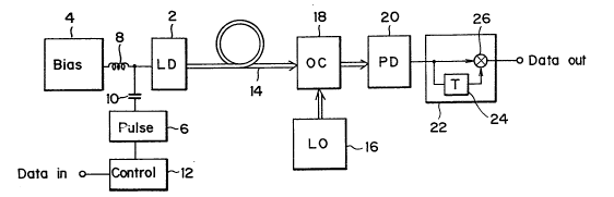
Figure 1 is a block diagram of a DM-PSK (direct
modulation phase shift keying) system as an embodiment of the
present invention;
Figure 2 is a block diagram of a CPFSK system as a prior
art example;
Eigure 3A is a drawing schematically showing a waveform
of a light output and a waveform of a frequency deviation in the
system shown in Flgure 1;
Figure 3B is a drawing schematically showing a
2 ~ 7 8
waveform of a light output and a waveform of a frequency
deviation in the system shown in FIG. 2;
FIG. 4, FIG. 5, FIG. 6, and FIG. 7 are
drawings showing waveforms of some si~nals in the CPFSK
system æhown in FIG. 2 at the times when m is equal to
0.5, 1.0, 1.5, and 2.0, respectively;
FIG. 8, FIG. 9, FIG. 10, and FIG. 11 are
drawings showing waveforms of some signala in the DM-PSK
system shown in FIG. 1 at the times when m is equal to
1.0, 1.5, 2.0, and 0.5, respectively;
FIG. 12 is a block diagram of a DM-PSK system
a8 another embodiment of the present invention;
FIG. 13 is a block diagram showing another
example of a demodulator in FIG. 12;
FIG. 14 is a block diagram of a DM-PSK sy~tem
a~ a further embodiment of the pre~ent inventioll; and
FIG. 15 i~ a block diagram showing another
example of a demodulator in FIG. 14.
DRSCRIPTION OF THE PREFERRED EMBODIMENTS
-Referring to FIG. 1, there i~ ~hown a DM-PSK
~ystem with the present lnvention applied thereto.
Reference numeral 2 denotes a laser diode in a DFB
(distributed feedbuck) type, and this laser diode 2
2 ~ 7 8
outputs a light beam corresponding to an injection
current. The in3ection current is supplied by means of
a bias current circuit 4 and a modulating current pulse
circuit 6. A DC current ~or biasing is supplied to the
la~er diode 2 through an inductor 8 and a high-speed
modulating current pulse is supplied to the laser diode
2 through a capacitor 10. The modulating current pulse
has.a pulse width smaller than one time slot of a
binary-coded input signal. An amplitude and pulse-width
control circuit denoted by 12 controls the amplitude and
pulse-width of the modulating current pulse according to
the data input 90 that the phase of the integrated
amount of the oscillation frequency of the laser diode 2
varied by the modulating current pulse may become ~ or
-~ at all times.
The light beam output of the laser diode 2 is
~ent to the reception ~ide through nn optical fiber 14.
Reference numeral 16 denotes a local oscillator formed
of a laser diode and it~ drive circuit. The local
oscillator 16 output~ a local light beam with a
frequency equivalent to or sl.ightly different from the
frequency of the light beam output from the laser diode
2 on the transmissioll side. The light beam transmitted
through the opticsl fiber 14 and the local light beam
.
.. ..
20) ~7~
are added up in an optical coupler 18 and input to a
photodetector 20. When the received light beam and the
local light beam together are input to the photodetector
20, an IF (intermediate frequency) signal includirlg the
5 transmitted~information in the form of a phase deviation
is generated by virtue of the square-law detecting
characteristic of the photodetector 20, and this IF
signal is input to a demodulator 22. The demodulator 22
divides the input IF signal into two portions and allows
one portion thereof to be delayed by a time T, which
corresponds to one time slot, by a delay circuit 24 and,
thereafter, mixed with the other portion in a mixer 26,
whereby a demodulated signal is output therefrom.
Since making the CPFSK system understood first
is considered helpful for describing the operation of
the system shown in FIG. 1, a block diagram of the same
is shown in FIG. 2. On the transmission side, Z8
denotes a laser diode whose oscillation frequency is
variable and 30 denotes a modulator for modulating the
o~cillation frequency of the laser diode. Here, the
deviation of the oscillation frequency is adjusted
according t-l the data input 90 that the phase deviation
between different ~igns become~ larger than ~ . A light
beam transmitted to the reception side through an
2 ~ 7 8
optical fiber 32 i8 added up with a local light beam
from a local oscillator 36 in an optical coupler 34 and
then subjected to a photoelectric transfer in a
photodetector 38. An IF signal generated by the
6 transfer i9 input to a demodulHtor 40, wherein it9 one
portion delayed by a predetermined period of time ~ in
a delay circuit 42 is mixed with the other portion in a
mixer 44 so thst a demodulation i9 performed. The delay
time ~ iB set up according to the modulation index m as
~ = T~2m, m = ~ F/B,
where T represents the time of one slot, a F represents
the frequency deviotion, and B represents the bit rate.
In this way, the CPFSK systsm iB arranged such that, on
its trRnsmission side, the laser diode is directly
modulated without using an external modulator and, on
its reception side, the phase deviation in the IF sign
is detected and thus the transmitted information i9
reproduced. Therefore, its system structure i9
relatively ~imple. However, the CPFSK system is
susceptible to the influence of wavelength dispersion
and, in addition, the carrier effective for clock
generation or the like cannot be reproduced therein.
FIG. 3~ and FIG. 3B are drawings schematically
showing waveforms of light outputs and waveforms of
.~ , . ,.,, ~.,
20 1~ 78
frequency deviations in the DM-PSK system of the present
invention and the CPFSK system, respectively. The
waveforms of light outputs in the drawings are depicted
with the oscillation frequency of the laEer diode
greatly reduced from the actual value. In the CPFSK
system, the frequency is uniformly deviated during the
period of time corresponding to one time slot T so thfft
the waveform of the light output may ~ot become
discontinuou~ at the junction of bits. On the other
hand, in the DM-PSK system, the oscillation frequency is
deviated by ~ F only during a predetermined period of
time I within one time slot T and thereafter the
o~cillation frequency is returned to the original
frequency. The value~ of I and ~ F, when the input
signal i~ a binary-coded signal, are set such that the
pha~e deviation after the time ~ will become ~ (- ~ ).
The value of ~ corresponds to the pul~e width of the
modulating current pulse.
The period of time during which the frequency
i9 deviated, the time delayed in the demodulation
proces~, and the preferred intermediate frequency are
shown in the following table for both the DM-PSK system
and the CPFSK aystem with the~e value~ arranged in
contrast with euch other.
12
2 ~ '7 8
TABLE
Present Invention CPFSK System
Time for Freq.
Deviation (1/2m)T lT
Delay Time in
Demodulation lT (l~Zm)T
Preferred
IF (2N + l)B/2(2N + l)mB/2
T: time ~lot
B: bit rate
m: modulstion index
(m = ~ F~B, a F: frequency deviation)
N: natural number
FIG. 4 to FIG. 7 are graphs showing results of
calculations of the signal waveforms in the CPFSK system
with the modulation index set to 0.5, 1.0, 1.5, and 2.0,
respectively. Conditions u~ed for the calculation~ are
as follows.
~ The rise time and the fall time of the
.input waveform are neglected and it is assumed tllat the
modulation is performed by a square wave.
~ The modulation index m is defined by
m ~ F/B, where B represents the bit rate and a F
, .:. ,.
201~78
represents the frequency deviation.
~ As a F, the maximum frequency deviation
a FMAX providing the highest reception sensitivity is
employed.
~ FMAX = 1/2l = mB (~ : delay time)
~ The intermediate frequellcy
fIF = (2N + 1)/(41 )
= ((2N + 1)/2)mB
(N - O, 1, 2, 3, ... )
~ Calculations are made with N = 2 when the
modulation index m = 0.5, 1Ø
~ Calculations sre made with N = 1 when the
modulation index m = 1.5, 2Ø
Throughout the drawings from FIG. 4 to FIG. 7,
(a) shows a code pattern for "01010", (b) shows a
waveEorm of the IF signal, (c) shows the phase of the IF
signal, aDd (d) shows the phase deviation referenced
from the ~ignal of code "O". What is shown here is a
case in which fIFo < fIFl~ where fIFo and fIFl
ZO respectivel~ represent the IF signal frequency of the
signal of code "O" snd that of the ~ignsl of code "1".
In the di~gram (d) 1B aleo shown the time to-l8o during
which the phase oE the IF signal makes a cumulative
change of ~ . Further, (e) show~ the phase of the IF
14
20 ~ ~78
signal (continuous line) and the phase of the IF signal
delayed by the delay time ~ (broken line) and (f) æhows
the demodulated waveform.
From results of the above described
calculations, following things are known.
~ While a '0 - ~ ' modulation is digitally
performed with respect to the phase of signal in the PSK
system, the modulation with respect to the frequency of
signal is digitally performed in the CPFSK system.
Therefore, the phase deviation develops as time
integration of the frequency deviation (refer to (d) in
the drawings) snd, when a modulation by a code "1" is
applied, the phase deviation (referenced from the ~ignal
of code "0") changes at a constant rate of change which
i8 determined by the frequency deviation. Further, the
period of time during which the demodulation is carried
out, i.e., the frequency deviation takes place, is one
time slot.
~ The time to-l8o required for the phase to
deviate ~ is obtained from (d) of each drawing as
tO-180 = T/2m~
which indicates that, the lnrger the frequency deviation
~ F (modulation index m) i~, the shorter the time to-l8o
required for the phase to deviate ~ becomes.
2 ~
The time to-l8o agrees with the delay time
in the demodulation of the IF signal.
In the DM-PSK ~ystem of the present invention,
in contraRt with the above described CPFSK system, ttle
injection current supplied to the laser diode i~ varied
only for 8 predetermined period of time shorter than one
~lot time in achieving the phsse deviation of ~ . At
the time of demodulation, a delayed demodulation by one
bit, for example, c~n be performed
FIG. 8 to FIG. 11 are grsph~ showing results
of cslculations of slgnal wsveforms in the DM-PSK system
with the modulstion index re~pectively set to 1.0, 1.5,
2.0, snd 0.5. Conditions used for the calculations are
as follow~.
~ The rise time and the fall time of the
input waveform are neglected and it is assumed that the
modulation is performed by a square wave.
~ A~ the intermediate frequency fIF = (N~2)B,
(N 3' 4' 5~ -- )~ fIF = 2B is used
Throughout the drawings, (a) shows a frequency
devistion for "01010", ~b) shows H waveform of the IF
signal, (c) shows the phase of the IF signal, and (d)
show~ the phase deviation referenced from the ~ignal of
code "0". What is shown here is 8 csse in which fIFo <
20 1 ~ 78
fIFl, where fIFo and fIFl respectively represent the IF
signal frequsncy of the signal of code "0" snd that of
code "1". Further, (e) shows the demodulated waveform.
Here, the demodulated waveform can be obtained from the
following calculation.
Considering that a delayed demodulation by
one--bit with a delay time T is performed using a mixer,
an IF signal f(t) is set as
f(t) = A co~(2~ (fIF + ~ F-M(t))t),
where M(t) is defiDed by
= 1 (in the case where the signal is of
code "1" and
M(t) NT < t < NT + I = NT + 1/(2m))
16 = 0 (in other cases),
where a F x 1/(2m) = ~ . If it i9 a~sumed that the
frequency characteri~tic of the u~ed receiver is flat
and no LPF (low pa~s filter) changing the demodulated
waveform (baseband signal) i~ used, then the demodulated
signal g(t) is expres~ed as
g(t) = f(t) x f(t - T)
= C co~(2~ fIF ~
+ a F(M(t - T) (t - T) - M(t)-t)),
where C is a con~tant.
20~ ~ 73
From the above results of calculations, the
following facts are known a~ to the DM-PSK system.
~ Whi].e a '0 - ~ ' modulation is digitally
perfnrmed with respect to the phase of the signal in the
PSK 3ystem using an external modulator, a modulation is
digitally performed with respect to the frequency of the
signsl in the DN-PSK system. Therefore, the phase
deviation of the signal develops a~ time integration of
the frequency deviation (refer to (d) in each drawing3
and, when a modulation by c code "1" is applied, the
phase deviation (referenced from the signal of code "0"3
changes with a constant gradient determined by the
frequency devistion until the phase deviation becomes
or -~ .
~ The time to-l8o required for the phase to
deviate ~ is obtained as
tO-180 = T/2m,
which indicates that, the larger the frequency deviation
a F (modulation index m3 i8, the shorter the time to-l8o
required for the phase to deviate ~ becomes.
~ The time to-l8o agree~ with the delay time
T in the demodulation of the IF ~ignal in the CPFSK
system.
When the DM-PS~ sy~tem i~ thus compared with
18
20 1 ~78
the CPFSK system, the frequencie~ of the signals in both
of the systems are changed without producing a
disconti~uous change of the phase of the signals, and
therefore, they are equal in that a direct modulation of
the laser diode is achieved therein without using an
external modulator. However, the DM-PS~ system
according to the present invention has an advantage over
the.CPFSX sy~tem that it i8 hardly affected by the
adverse influence of the wavelength dispersion. More
specificslly, when the CPFSK ~ystem iY used, at -the time
point where the eye pattern of the demodulsted waveform
open~, the frequency providing the demodulated signal of
"1" and the frequency providing that of "0" are
different and, therefore, a code error due to the
wavelength dispersion is liable to occur. In contrast
with that, according to the present invention, when for
example the modulation index is rçlatively great as
shown in FIG. lO, the frequency providing the
demodulated signal of "1" and the frequency providing
that of "0" are iD agreement at the time point where the
eye pattern of the demodulated waveform opens, and
therefore, the deterioration in the code error rate due
to the wavelength dispersion hardly occurs.
In contrast with the DPSK By~tem~ a delayed
. ~, ., . i
203 ~78
demodulatioll by one bi-t csn be simply performed in the
present invention without using a differential coding
circuit on the tran~mi~ion ~ide. While the upper ]imit
of the modulation band has conventionally been
determined by the performance of the pha~e modulator, a
still higher speed can be achieved in the present
invention by virtue of the capability of the direct
modulation.
In the present invention, the deviation of the
oscillation frequency of the laser diode during only a
predetermined period of time ~ , which is shorter thun
one time slot, can be provided by having an RZ signal
with a suitable duty cycle generated by the amplitude
snd pulse width control circuit 12.
Since it is possible to perform a direct
modulstion of the laser diode in the ~ystem shown in
FIG. 1, an external modulator i9 not Decessary, and
since a modulating current pulse is supplied to the
la~er diode so that the phase deviation between -the
Z0 different clgns may become ~ or -~ , a differential
coding circuit i~ not required.
FIa. 12 i3 a block dlagram ~howing a DM-PSK
cystem a8 another preEerred embodiment of the present
invention. In this system, there i~ used a demodulator
~0
2~1 9~78
different from that in the preceding embodiment. In the
demodulator 46 of the presen-t embodiment, 48 denotes a
frequency doubler for doubling the frequency of the
input IF signal and 50 denotes a frequency halver for
halving the frequency of the signal with the frequency
once doubled by the frequency doubler 48. The IF
signal, by being passed through the frequency doubler 48
and frequency halver 60 in order of mention, is deprived
of its modulstion component and the carrier i~
reproduced. Hence, by performing mixing of this carrier
with the IF ~ignal not deprived of the modulation
portioIl in a mixer 52, a synchroni~ed demodulation c~n
be achieved. In this case, by providing, a5 shown in
FIG. 13, a delay circuit 49, which will introduce a
delay time corresponding to the delay time given to a
signal pa~sed through carrier reproducing means 47
formed of the frequency doubler 48 and the frequency
halver 60, phase noise can be suppressed and reception
with a high ~ensibility can be achieved.
FI~ i8 a block diagram showing a DM-PSK
sy~tem as a further embodiment of the present invention.
In thi3 system, there are used e modulating current
pulse circuit 64, an amplitude and pulse width control
circuit 66, und a demodulator 68 of structure or
21
2 ~ 8
operation different from those in the previou~
embodiments are used. The modulating current pulse
circuit 54 superposes a mDdulating current pulse with a
~maller pulse width than one time slot of an n-value-
coded input signal (n: a natural number larger than 2)on the bias current. The amplitude and pulse width
control circuit 56 controls the amplitude and pulse
width of the modulating current pulse so that the
integrated value of the oscillation frequency of the
laser diode 2 varied by the modulating current pulse may
become 2~ k/n or -2~ k/n (k = 1, 2, ... , (n - 1)) as a
phase amount. The control circuit 56 iB supplied, for
example, with a four-value signal. The co~ltrol circuit
56 performs control of the waveform of the modulating
current pulse so that a frequency deviation msy not be
caused in a first state of the four-value states and, iD
second to fourth states, the pha~e deviation may
respectively become 2~ k/4 (k = 1, 2, 3) with respect to
the first state. More specifically, if, in the present
exsmple, the state of the phase corresponding to one of
the four-vulue signals is 0, then the other three ~tates
of the pha~e become ~ /2, ~ , and 3~ /2, respectively.
In the demodulator 6B, numeral 60 denotes a
frequency quadrupler for quadrupling the frequency of
22
2 ~ 7 8
the input IF signal, numeral 62 denotes a frequency
quaterer for quartering the ~requency of the output of
the frequency quadrupler 60~ numeral 64 deno-tes a phase
shifter for shifting the phase of the output of the
frequency quaterer 6Z by ~ /4, numeral 66 denotes a
phase shifter for shifting the output of the frequency
quaterer 62 by -~ /4, numeral 68 denote~ a mixer for
mixing the output of the pha~e shifter 64 and the IF
signal, and numeral 70 denotes a mixer for mixing the
output of the phase shifter 66 and the IF signal. A
demodulation is performed in accordance with the carrier
reproduced by the frequency quadrupler 60 and frequency
quaterer 62, and first and second outputs are obtained
from the mixers 68 and 70, respectively. Thereupon, by
combining the first and ~econd outputs, four-value
signals can be reproduced.
Since such a DM-PSK system dealing with many
value (many phase) signal is susceptible to the
influence of phase noise of the light source, by
providing, a9 ehown in FI~. 15, delay circuits 72 and 74
of ~imilar ~tructure to that of FIa. 13 for delaying the
re~pective IF signa1~ input to the mixers 68 and 70 by
predetermined amount~, the phase noise can be removed
gulte effectively and reception with a high sensitivity
2 ~ 7 8
can be achieved.
According to the system or method of the
present invention, different from the case of the CPFSK
systeml the carrier can be reproduced, and therefore, a
synchronized demodulation can be performed as described
with FIG. 12 aDd FIG. 13. Further, as described with
FIG. 13, generation of many-value signals can be easily
achieved. Specifically, when many-value signals are
obtained, the range of the spectrum becomes narrower
than that in the case where many-vHlue signals are
obtained in other systems, and therefore, in carrying
out frequency-division multiplexing, the number of
channels in the system can be increased and in addition
the system i9 hardly affected by an adverse influence of
the wavelength dispersion.
While the above description has been mode as
related to specific embodiments, it is to be understood
that the present invention is not limited to the details
of these embodiments. For example, in the preferred
embodiments shown in the drawings, description has been
mHde of the case where the ~ignal iB binary-coded or ~-
value-coded, but an 8-value or 16-value-coded signal may
be used in order to increase the tran~mission capacity.
A demodulation using a filter of a narrow band m~y be
24
213 1 ~ ~8
performed thereby reproducing the carrier. Thus,
preferred embodiments described herein are given by way
of illustration only and not limitative of the present
invention. The scope of the invention iB defined by the
appended claims and all changes and modifications as
fall within the equivalence of the scope of the claims
are therefore to be embraced by the invention.