Note: Descriptions are shown in the official language in which they were submitted.
FAULT TOLERANT MEMORY
Field of the Invention
The present invention relates to data storage
techniques., and more particularly to methods for
organizing data in a memory to optimize the memory's
tolerance for system faults.
background of the Invention
Error correction codes (Ekes) have been used to
protect data stored in memory systems such as dynamic
random access memories (DRAM's). Hamming codes are
commonly used for this purpose. Although Hamming codes
are useful to protect the DRAM's from acquiring "soft"
errors, such as those due to the effects of Alpha
particles, they do not protect against complete device or
data bus failures in the systems
The utilization of a ten bit multi burst error
correcting Reed-Solomon code has been found to be
effective in protecting static RAM (SWAM) or DRAM data
from "hard" errors due to memory device or data bus
failures However, the ten bit Reed-Solomon EKE
encoder/decoder must have its ten bit wide data bus
interfaced with the data bus of the memory system, which
is sixteen bits wide. Furthermore, the ten bit EKE
symbols must be stored in the SWAM or DRAM in storage
locations which are multiples of eight bits This causes
each ten bit symbol to overflow into more than one storage
location. Thus, failure of one storage location can cause
the failure of two ten bit symbols, which can degrade the
performance of the corresponding EKE. Although extra
memory storage locations can be provided to insure that
the failure of one storage location cannot cause the
failure of more than one ten bit symbol, this is wasteful
of memory.
Summary of the Invention
In the preferred embodiment, the present
invention organizes ten-bit EKE symbols for storage in
memory devices having eight-bit bytes. Ten-bit Reed-
Solomon symbols are created by an encoder/decoder and are
present on a ten-bit bus. A data converter converts the
symbols so that they are conveyable via a sixteen-bit bus,
with all of the ten bits Ox each ten-bit symbol being
conveyable via one of the sixteen bits of the bus. A 640
byte Reed-Solomon data block is stored in twenty byte
groups of each of thirty-two eight-bit by 12~ kilobyte
static RAM devices. The thirty-two RAM devices are
organized in two columns of sixteen with all devices of
one column receiving the eight least significant bits of
the sixteen bit bus and all devices of the other column
receiving the eight most significant bits of the sixteen
bit bus. The ten-bit symbols are organized vertically in
the RAM devices Jo that the same bit positions of ten
different bytes of a given RAM device contain the ten bits
of a ten-bit symbol. Each of the thirty-two RAM devices
contains only sixteen vertically organized ten-bit symbols
within a group of twenty bytes so that any two devices can
fail, or any one bit of the sixteen bit bus can fail, and
the Reed-Solomon EKE will preserve all data.
Description of the Drawings
Figure 1 is a prior art scheme for accommodating
ten bit symbols in devices having multiples of eight bits.
Figure 2 is a block diagram of a memory system
including an EKE system which is suitable to use in the
present invention.
Figure 3 is a block diagram illustrating the
organization of memory according to the present invention.
Description of the Preferred Embodiment
Referring to the drawings, wherein like
reference characters designate like or corresponding parts
throughout the views, Fig. 1 is a block diagram of the
prior art scheme for accommodating ten-bit Reed-Solomon
symbols on a bus or device with multiples of eight bits.
Ten-bit symbol pa comprises bits 0-9, symbol 2b comprises
bits 10-19, symbol 2c comprises bits 20-29 and symbol Ed
comprises bits 30-39. The four ten-bit symbols pa through
Ed are loaded into five consecutive eight-bit random
access memory bytes pa through ye, to accommodate the
symbols in the forty bits provided by the five memory
bytes pa through ye. The alignment between the symbols
and the bytes is also shown, with byte pa comprising bits
0-7, 4b comprising bits 8-15, 4c comprising bits 16-23, Ed
comprising bits 24-31 and ye comprising bits 32~39. Byte
pa and byte ye include only one symbol, all other RAMS
--4--
4b-4d include more than one symbol. Thus if any of the
bytes 4b through Ed fail, two of the symbols pa through Ed
are lost. A fault tolerant memory can be organized based
upon this scheme, but more memory bytes must be used.
Figure 2 is a block diagram of a memory system
including an EKE system which is suitable to use in the
present invention. A memory system 6, such as a cache for
a central processing unit (CPU) or a storage device,
includes a memory array 8. The memory array 8 typically
has an array of 32 static random access memory devices
(ROME) which are each eight bits wide by 128 kilobytes
long to provide a total memory capacity of 4 megabytes
(4,194,304 bytes). The memory array 8 transfers its data
on a 16 bit wide input/output data bus 10.
The 10 bit Reed-Solomon EKE used with the memory
array 8 is provided by an EKE encoder/decoder 12. The
encoder/decoder 12 decodes and encodes ten bit symbols
transferred on a ten bit data bus I The symbols on the
data bus 14 are not suitable for coupling to the memory
array 8 via the data bus 10. This is because the data bus
10 is sixteen bits wide and the data bus 14 is ten bits
wide. Furthermore, the ten bit symbols on the data bus 14
must be aligned with the bytes of the RAM's in the memory
array 8 to avoid wasting memory bits in the RAM's of the
memory array 8.
A data converter 16, coupling the data bus 10 to
the data bus 14, provides the necessary bit conversion,
data alignment and storage organization to maximize the
fault tolerance of the storage device when used in
conjunction with an error correcting code (EKE). The data
converter 16 also optimizes the fault tolerance for the
- s -
EKE encoder/decoder 12 so that either two of the 32 RAM'S
in the memory array B or one data bus bit of the data bus
10 can fail without loss of data.
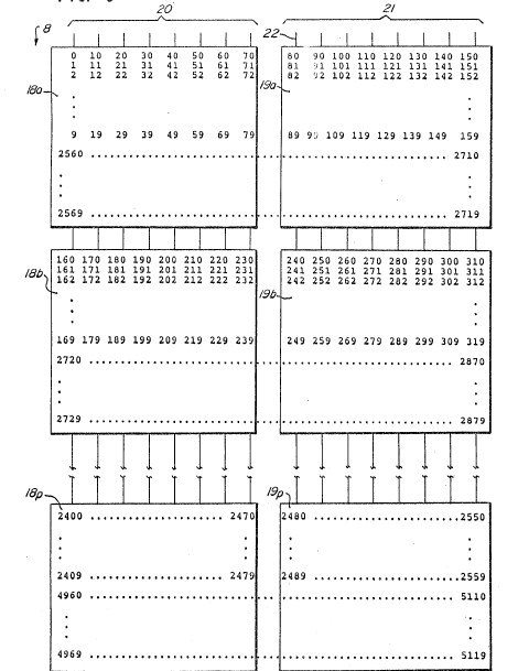
Figure 3 illustrates the organization of data
within memory array 8. For clarity, the organization of
only one 640 byte block of EKE encoded data is shown,
although it should be understood that the entire contents
of memory array 8, which may be 4 megabytes, is similarly
organized. Data converter 16, in Fig. 2, provides the
conversion between standard Reed-Solomon ten-bit symbols
on bus 14 and the code illustrated in Fig. 3. With an
understanding of the data organization of Fig. 3,
therefore, data converter 16 may be implemented in any one
of a number of well known ways, such as by way of a simple
gate array having special memory cells organized in an
array of ten rows and sixteen columns where ten-bit
symbols are written to successive columns until the array
is full and then sixteen-bit data is read from the rows
and appears on data bus lo
The memory array 8 comprises any suitable number
of RAM's of which thirty-two RAM's aye through 18p and lea
through lop are illustrated and are used to store one 640
byte block of data according to the present invention,
Twenty memory bytes or storage locations, each having
eight bits, of each RAM aye through 18p and lea through
lop are illustrated and are used to store one 640 byte
block of encoded data. The thirty-two Amos are arranged
in two columns of sixteen, with all RAM's of one column,
RAM's aye through 18p, receiving the least significant
eight bits, shown at 20~ of sixteen-bit data bus 10 and
all RAM's of the other column, RAM's lea through lop,
receiving the most significant eight bits, shown at 21, of
.
--6--
sixteen-bit data bus 10. Each memory byte is illustrated
as a horizontal eight-bit line within the respective I
Other blocks of 640 bytes of encoded data are stored in
other groups of twenty bytes in the respective RAM's.
The encoded data 13 is converted by data
converter 16 so that it is stored in memory array 8 in an
interleaved fashion. As shown in Fig. 3, the first ten-
bit symbol, comprising bits 0 through 9 which are simply
illustrated in Fig. 3 as the numerals 0 through 9,
occupies the first bit positions of the first ten bytes of
RAM aye respectively. Likewise, the second ten-bit
symbol, comprising bits 10 through 19, occupies the second
bit positions of the first ten bytes of RAM aye
respectively. This pattern of organization continues such
that all eight bit positions of the first ten bytes of RAM
aye are occupied with the first eight ten-bit symbols.
By way of further examples, the ninth ten-bit
symbol is received by RAM aye via the least significant of
most significant lines 20, shown at 22, and occupies the
first bit positions of the first ten bytes of RAM lea
respectively. The Thea ten-bit symbol occupies the
eighth bit positions of the first ten bytes of RAM 19p,
and the Thea ten-bit symbol occupies the first bit
position of the second ten bytes of RAM aye. The last or
Thea ten-bit symbol occupies the eighth bit positions of
the second ten bytes of RAM lop respectively.
With the data organization described above, only
sixteen ton bit symbols are stored in each of the RAM's
18, 19. Since the ten bit Reed-Solomon EKE can correct 3
of the ten bit symbols, two of the RAM's 18 can fail
without loss of data. Alternatively, a failure of one of
the bits 20, 21 of the sixteen bit date bus 10 can occur,
resulting in the loss of 32 of the ten-bit symbols without
loss of data.
The fault tolerances of the memory system 6
descry bed above are optimal and may be represented by the
relationship:
RAM's failed = Bits correctable by EKE
Total RAM's Total bits in data block 16
The vertical symbol scheme also allows:
Bus bits failed = Bits correctable by EKE
Total bus bits Total bits in data block 16
ox course, other conversion schemes can be
implemented in accordance with the present invention, and
it is within the scope of the invention to provide for
storing and transferring data symbols with any first
number of bits sequentially fed on each bit of a data bus
of a second number of bits to data of the second number of
bits in length on each bit of a data bus of the first
number of bits to provide optimum data organization. In
particular, since most memory devices have words in
multiples of bytes, or eight bits, the present invention
is particularly advantageous in converting ten bit symbols
on ten bit data bases to data on a data bus of eight,
sixteen, thirty two, or more bits,
Thus there has been described herein a method of
optimizing the organization of data comprising symbols
with a first number of bits transferred between a first
data bus having a second number of bits and a second data
bus having the first number of bits with optimal fault
tolerance and automatic symbol alignment.
It will be understood that various changes in
the details, arrangement and configuration of the parts
and systems which have been described and illustrated
above in order to explain the nature of the present
invention may be made by those skilled in the art within
the principle and scope of the present invention as
expressed in the appended claims.
What is claimed is: