Note: Descriptions are shown in the official language in which they were submitted.
2019368
1 TITLE OF THE INVENTION
ATM SWITCHING SYSTEM HAVING DUAL ATM SWITCH
STRUCTURE
BACKGROUND OF THE INVENTION
The present invention generally relates to an
ATM (asynchronous transfer mode) switching system
having a dual ATM switch structure.
There is a limit on the bit rate of data
transmission in a conventional switching system by the
use of public lines. From this point of view, there
has been considerable activity regarding the
development of an ATM switching system which can
transfer data at higher bit rates.
In an ATM switching system, data is divided
into cells. One cell is the unit of data
transmission. A header is included in each cell having
data. The ATM switching system selects a data
transmission route by means of hardware in accordance
with the contents of the header. The ATM switching
system can provide a large number of data transmission
routes, which are realized by buffers.
Generally, two identical primary structural
elements in a switching system are provided in order to
realize high reliability. For the same purpose, it is
desirable that the number of primary structural
elements in even ATM switching systems be doubled. A
conventional ATM switching system has a plurality of
storing buffers arranged in a matrix, and each of the
buffers is capable of storing a plurality of cells.
Each buffer can always accept input cells successively
and output cells successively. In other words, cells
are successively input to each buffer, while each
buffer also outputs cells successively. In a case
where the ATM switching system has two identical ATM
switches and these ATM switches are in service, it is
necessary for the two in-service ATM switches to
2019368
operate in the same way. That is, the two ATM switches must
have the same operatlng state. In this case, one of the two
ATM switches which are in service serves as a master ATM
switch and the other ATM switch serves as a slave ATM swltch.
Since the master ATM switch and the slave ATM switch
operate ln the same way, lt ls posslble to switch the ATM
swltches from the master ATM swltch (ln a master mode) to the
slave ATM swltch (ln a slave mode) when a fallure occurs ln
the master ATM swltch. The ATM swltch in which a failure
takes place ls set to the out-of-service state and is
lnvestlgated. After the failure in the ATM switch ls
ellmlnated, lt ls swltched from the out-of-servlce state to
the ln-service state. It should be noted that at thls tlme
there ls no cell in the ATM switch. That is, the contents of
the ATM swltch whlch will be set to the in-servlce state are
dlfferent from those ln the master ATM swltch whlch ls
operatlng. Thus, even when the ATM swltch ls switched from
the out-of-servlce state to the in-service state, it is
lmposslble to set the ATM swltch to the master ATM switch. As
a result, lt ls desired to overcome the above-mentloned
problem.
SUMMARY OF THE INVENTION
It ls a general ob~ect of the present lnventlon to
provlde an lmproved ATM swltchlng system ln whlch the above-
mentloned disadvantage ls elimlnated.
A more speclflc ob~ect of the present lnventlon ls
to provlde an ATM swltchlng system ln whlch one of the two ATM
swltches ln the out-of-service state can serve as the master
-, 27879-27
;,~
~ ~f
2019368
switch system lmmediately after it ls switched from the out-
of-service state to the in-servlce state.
In accordance with the present lnvention there is
provided an ATM (asynchronous transfer mode) switching system
comprising: a first ATM switch having input lines and output
lines; a second ATM switch having lnput llnes and output
lines, sald flrst ATM swltch having a structure identical to
sald second ATM swltch; lnput means, coupled to said flrst and
second ATM switches, for supplying cells via an input
transmlsslon llne to sald input llnes of sald flrst and second
ATM switches; and select means, coupled to said first and
second ATM swltches, for selecting elther one of sald flrst
ATM swltch or said second ATM swltch so that the output lines
of a selected one of the flrst and second ATM swltches are
coupled to an output line extending from said ATM switching
system and operates a master mode, whereln each of said flrst
and second ATM switches includes; buffer means, provlded at a
crosspolnt where a correspondlng one of sald lnput llnes and a
correspondlng one of sald output llnes cross, for temporarlly
storlng sald cells supplied from said corresponding one of the
lnput llnes and for outputtlng sald cells to sald corre-
sponding one of the output llnes; counter means, coupled to
said buffer means, for counting a number of said cells ln sald
buffer means and for outputting a counter value indicative of
the number of said cells; different calculating means provided
for each of the first and second ATM switches, and coupled to
said counter means of said flrst ATM switch and said counter
means of said second ATM switch, for calculating a difference
27879-27
'~'
- 2ol9368
between the counter values ln said counter means of said first
and second ATM swltches when sald selected one of the flrst
and second ATM swltches ls in an in-service state and the
other one of sald flrst and second ATM swltches ls ln an out-
of-servlce state; and dummy cell generatlng means, coupled to
sald dlfference calculatlng means and said buffer means, for
generatlng a number of dummy cells corresponding to said
difference produced by said difference calculatlng means and
for writing said dummy cells into said buffer means of the
other one of the flrst and second ATM switches whlch ls in the
out-of-servlce state so that the other one of the first and
second ATM switches in the out-of-service state ls changed to
a slave mode from the out-of-servlce state, and whereln sald
ATM swltchlng system further comprlses control means coupled
to the counter means of each of the flrst and second ATM
swltches, and the select means, for determlnlng whether or not
said dummy cells in sald buffer means of the other one of the
first and second ATM swltches ln the slave mode have been
output therefrom, so that when it ls determined by said
control means that all of said dummy cells have been output
from said buffer means, the first and second ATM switches are
synchronized with each other, and for controlling the selector
means to execute the swltching between the first and second
ATM switches after all of the dummy cells have been output
from the buffer means of the other one of the first and second
ATM swltches.
In accordance wlth the present invention there is
also provlded an ATM (asynchronous transfer mode) switchlng
27879-27
2019~68
system comprlslng; a first ATM switch having input lines and
output lines; a second ATM swltch havlng input lines and
output lines, said first ATM switch havlng a structure
ldentlcal to sald second ATM swltch; lnput means, coupled to
sald first and second ATM switches, for supplying cells via an
lnput transmlssion llne to said input lines of sald first and
second ATM switches; and select means coupled to said first
and second ATM switches, for selecting either one of sald
first ATM switch or said second switch so that the output
lines of a selected one of the first and second ATM swltches
are coupled to an output transmission line extendlng from said
ATM switching system and operates in a master mode, wherein
each of said flrst and second ATM switches includes; buffer
means, provided at a crosspoint where a correspondlng one of
sald lnput lines and a correspondlng one of sald output llnes
cross, for temporarlly storlng sald cells supplied from said
corresponding one of the input lines and for outputting said
cells to said corre-sponding one of the output lines; counter
means provlded for each of sald flrst and second ATM switches,
and coupled to said buffer means, for countlng a number of
said cells in sald buffer means and for outputtlng a counter
value lndicative of the number of said cells, said counter
value in said counter means of said selected one of the flrst
and second ATM swltches whlch is in an ln-servlce state belng
wrltten into said counter means of the other one of the first
and second ATM swltch whlch ls ln an out-of-servlce state so
that the other one of the flrst and second ATM swltch is
changed to a slave mode from the out-of-service state; and
2787~-27
"" ~
2019368
difference calculating means provided for each of the first
and second ATM switches, and coupled to said counter means of
said first ATM switch and said counter means of said second
ATM switch, for calculating a dlfference between the counter
values in sald counter means of sald first and second ATM
switches when sald selected one of the first and second ATM
switches is in the ln-service state and the other of the first
and second ATM switches is ln the out-of-service state, and
whereln said ATM swltchlng system further comprlses control
means coupled to the counter means of each of the flrst and
second ATM swltches, and the select means, for determlnlng
whether a number of cells whlch corresponds to the counter
value wrltten lnto sald buffer means of the other one of the
flrst and second ATM swltches whlch is in the slave mode has
been output from sald buffer means, so that when lt ls
determined by said control means that sald number of cells has
been output from sald buffer means in the slave mode, the
first and second ATM switches are synchronized with each
other, and for controlling said select means to execute
swltching between sald flrst and second ATM swltches.
In accordance wlth the present lnvention there is
further provlded an ATM swltchlng system (asynchronous
transfer mode~ comprising: a flrst ATM switch having input
lines and output llnes; a second ATM swltch havlng lnput lines
and output lines, sald first ATM switch havlng a structure
ldentlcal to sald second ATM swltch, each of sald flrst and
second ATM swltches including buffer means, provlded at a
crosspoint where a corresponding one of ~ald input llnes and a
27879-27
2019368
correspondlng one of said output lines cross, for temporarlly
storing cells supplled from said correspondlng one of the
input lines and for outputting said cells to sald
corresponding one of the output llnes; lnput means, coupled to
sald first and second ATM swltches, for supplying said cells
via an lnput transmisslon line to said input lines of sald
flrst and second ATM switches; select means, coupled to said
flrst and second ATM swltches, for selecting elther one of
said first ATM swltch or sald second ATM switch so that the
output lines of a selected one of the first and second ATM
switches are coupled to an output transmittion line extending
from said ATM swltchlng system and operates ln a master mode;
dummy cell generating means, coupled to sald flrst and second
ATM swltches, for generatlng a predetermlned number of dummy
cells and for writing said dummy cells into sald buffer means
of the other one of the first and second ATM switches which is
in an out-of-service state; and control means coupled to said
select means, and coupled to sald flrst and second ATM
swltches, for determining whether all of said dummy cells have
been output from said buffer means after the other one of the
first and second ATM switches is changed from said out-of-
service state to a slave mode, the other one of said flrst and
second ATM swltches operating in an in-service state where
sald selected one of the first and second ATM switches is in a
master mode, so that when it is determlned by said control
means that all of sald dummy cells have been output from said
buffer means, the flrst and second ATM swltches are
synchronized with each other, and for controlling the select
27879-27
` 201~3G8
means to execute the swltchlng between the first and second
ATM swltches after all of the dummy cells have been output
from the buffer means of the other one of the first and second
ATM swltches.
In accordance wlth the present lnventlon there ls
provlded an ATM swltchlng system (asynchronous transfer mode)
comprlslng: a flrst ATM swltch havlng lnput llnes and output
llnes; a second ATM swltch havlng lnput llnes and output
llnes, sald flrst ATM swltch havlng a structure ldentlcal to
sald second ATM swltch, each of sald flrst and second ATM
swltches lncludlng buffer means, provlded at a crosspolnt
where a correspondlng one of sald lnput llnes and a
correspondlng one of sald output llnes cross for temporarlly
storlng cells supplled from sald correspondlng one of the
lnput llnes and for outputtlng sald cells to sald
correspondlng one of the output llnes; lnput means, coupled to
sald flrst and second ATM swltches, for supplylng sald cells
vla an lnput transmlsslon llne to sald lnput llnes of sald
flrst and second ATM swltches; select means, coupled to said
flrst and second ATM swltches, for selectlng elther one of
sald flrst ATM swltch or sald second ATM swltch so that the
output llnes of a selected one of the flrst and second ATM
swltches are coupled to an output transmlsslon llne extendlng
from sald ATM swltchlng system and operates ln a master mode;
counter means, coupled to sald flrst and second ATM swltches,
for countlng a number of cells ln sald buffer means of sald
selected one of the flrst and second ATM swltches whlch ls ln
an ln-servlce state so that sald selected one of the flrst and
7a
. 27879-27
~,
201~3G8
second ATM switches operates ln a master mode; and control
means coupled to sald select means, and coupled to sald flrst
and second ATM swltches and sald counter means, for
determlnlng whether a number of cells which ls equal to sald
number of cells counted by sald counter means has been output
from sald buffer means of the other one of the flrst and
second ATM switches after the other one of the flrst and
second ATM swltches ls changed from an out-of-servlce state to
a slave mode, so that when lt ls determlned by sald control
means that said number of cells has been output from sald
buffer means ln the slave mode, the flrst and second ATM
swltches are synchronlzed wlth each other, and for controlllng
sald select means to execute swltchlng between sald first and
second ATM swltches.
In accordance with the present lnventlon there ls
also provlded a method for determlnlng that data stored ln a
buffer of a flrst ATM (asynchronous transfer mode) swltch ls
ldentlcal to data stored ln a buffer of a second ATM swltch,
comprlslng the steps of: a) countlng a total amount of data
stored in the buffer of the flrst ATM swltch; b) lnputtlng
ldentical lnput data lnto the buffers of the flrst and second
ATM swltches when lnput data ls present; c) outputtlng
correspondlng output data from the buffers of the flrst and
second ATM swltches; d) countlng an amount of correspondlng
output data output from the buffers of the flrst and second
ATM swltches ln sald step (c); e) comparlng the amount of
correspondlng output data output from the buffers of the flrst
and second ATM swltches counted ln sald step (d) wlth the
7b
27879-27
Y~
,~
- 2019368
total amount of data counted ln said step (a); f) determinlng
that the data ln the buffer of the flrst ATM switch ls
ldentical to the data ln the buffer of the second ATM swltch
when sald comparlng of sald step (e) lndlcates that the amount
of data output from the buffers of the first and second ATM
swltches counted ln sald step (d) ls greater than or equal to
the total amount of data counted in sald step (a); and g)
repeating said steps (b)-(f) when sald comparing of said step
(e) indlcates that the amount of data output from the buffers
of the flrst and second ATM swltches counted ln said step (d)
is less that the total amount of data counted in sald step
(a).
In accordance wlth the present lnvention there ls
further provlded a method for determlnlng that data stored in
a buffer of a first ATM (asynchronous transfer mode) swltch ls
ldentlcal to data stored ln a buffer of a second ATM swltch,
comprlslng the steps of: a) countlng a total amount of data
stored ln the buffer of the first ATM swltch; b) lnputtlng
dummy data to the buffer of the second ATM switch based on the
total amount of data counted in sald step (a); c) inputtlng
identical lnput data lnto the buffers of the first and second
ATM switches when input data is present; d) outputtlng
correspondlng output data from the buffers of the flrst and
second ATM swltches; e) countlng an amount of correspondlng
output data output from the buffers of the flrst and second
ATM swltches ln sald step (d); f) comparlng the amount of
corresponding output data output from the buffers of the flrst
and second ATM swltches counted ln sald step (e) wlth the
7c
,~ 27879-27
201!~368
total amount of data counted ln sald step (a); g) determlnlng
that the data ln the buffer of the flrst ATM swltch ls
ldentlcal to the data ln the buffer of the second ATM switch
when said comparlng of sald step (f) lndlcates that the amount
of data output from the buffers of the flrst and second ATM
swltches counted ln sald step (e) ls greater than or equal to
the total amount of data counted ln sald step (a); and h)
repeatlng sald steps (b)-(g) when sald comparlng of sald step
(e) lndlcates that the amount of data output from the buffers
of the flrst and second ATM swltches counted ln sald step (e)
ls less than the total amount of data counted ln sald step
(a).
In accordance with the present lnventlon there ls
provlded a method for determlnlng that data stored ln a buffer
of a flrst ATM (asynchronous transfer mode) swltch ls
ldentlcal to data stored ln a buffer of a second ATM swltch,
comprlslng the steps of; a) countlng a total amount of data
stored ln the buffer of the flrst ATM swltch~ b) countlng a
total amount of data stored ln the buffer of the second ATM
swltch; c) determlnlng a dlfference between the total amount
of data stored ln the buffer of the flrst ATM swltch and the
total amount of data stored ln the buffer of the second ATM
swltch; d) lnputtlng dummy data lnto the buffer of the second
ATM swltch based on the dlfference of the step (c); e) ln-
puttlng ldentical input data lnto the buffers of the flrst and
second ATM swltches when lnput data ls present; f) output-tlng
correspondlng output data from the buffers of the flrst and
second ATM swltches; g) countlng an amount of correspondlng
7d
27879-27
V
201~368
output data output from the buffers of the flrst and second
ATM swltches ln said step (f); h) comparlng the amount of
correspondlng output data output from the buffers of the flrst
and second ATM swltches counted ln sald step (g~ wlth the
total amount of data counted ln sald step (a); 1) determlnlng
that the data ln the buffer of the flrst ATM swltch ls
ldentlcal to the data ln the buffer of the second ATM swltch
when sald comparlng of sald step (h) lndlcates that the amount
of data output from the buffers of the flrst and second ATM
swltches counted ln sald step (g) ls greater than or equal to
the total amount of data counted ln sald step (a); and ~)
repeatlng sald steps (e) - (1) when sald comparlng of sald
step (h) lndlcates that the amount of data output from the
buffers of the flrst and second ATM swltches counted ln sald
step (g) ls less than the total amount of data counted ln sald
step (a).
2787g-27
2019368
-- 8
1 BRIEF DESCRIPTION OF THE DRAWINGS
Other objects, features and advantages of the
present invention will become apparent from the
following detained description when read in conjunction
with the accompanying drawings, in which:
FIGS.lA through lE are diagrams illustrating
a conventional ATM switching system having a dual ATM
switch structure;
FIG.2 is a block diagram of the entire
structure of an ATM switching system having a dual ATM
switch structure according to the present invention;
FIG.3 is a block diagram of a crosspoint
switch arranged at a crosspoint in one of the two ATM
switches in the ATM switching system shown in FIG.2 and
a crosspoint switch at the corresponding crosspoint in
the other ATM switch;
FIG.4 is a block diagram of a crosspoint
switch arranged at a crosspoint in one of the two ATM
switches in the ATM switching system shown in FIG.2 and
a crosspoint switch at the corresponding crosspoint in
the other ATM switch according to a first preferred
embodiment of the present invention;
FIGS.5A through 5E are diagrams illustrating
the operation of the first preferred embodiment of the
present invention shown in FIG.4;
FIG.6 is a block diagram of a crosspoint
switch arranged at a crosspoint in one of the two ATM
switches in the ATM switching system shown in FIG.2 and
a crosspoint switch at the corresponding crosspoint in
the other ATM switch according to a second preferred
embodiment of the present invention;
FIGS.7A through 7E are diagrams illustrating
the operation of the second preferred embodiment of the
present invention shown in FIG.6;
FIG.8 is a block diagram of a crosspoint
switch arranged at a crosspoint in one of the two ATM
switches in the ATM switching system shown in FIG.2 and a
20 199368
1 crosspoint switch at the corresponding crosspoint in
the other ATM switch according to a third preferred
embodiment of the present invention, and;
FIGS.9A through 9E are diagrams illustrating
the operation of the third preferred embodiment of the
present invention shown in FIG.8.
DESCRIPTION OF THE PREFERRED EMBODIMENTS
For the sake of understanding the present
invention, a description will now be given of a
conventional ATM switching system. Referring to
FIG.lA, there is illustrated the principle of an ATM
switch. The ATM switch is of a cross-bar type. The
ATM switch in FIG.lA has four inputs XO - X3 and four
outputs Y0 - Y3. Input lines carry inputs X0 - X3 and
output lines carry outputs Y0 - Y3. A cell switching
operation is carried out at crosspoints between the
input lines and output lines, which are indicated by
marks "*". A buffer is provided at each of the
crosspoints. Input cells XO - X3 on the input lines
are written into the buffers at the crosspoints between
the selected outputs lines and the input lines. For
example, when the output Y2 is selected, an input cell
at the input X1 is stored in the buffer at the
crosspoint of the input line related to X1 and the
output line related to Yl. As has been described
previously, each input cell has a header and data. The
header includes information indicating which route
should be selected. This information is analyzed at
each of the crosspoints. When a controller provided in
each of the crosspoints together with the buffer
determines that the header of an input cell indicates a
route related to its own, the controller controls the
buffer so that it stores the input cell.
FIG.lB illustrates the structure of an ATM
switch structure which has two inputs and two outputs.
The ATM switch structure shown in FIG.lB has four
~lo~
2019~68
1 crosspoint switches SWll, SW12, SW21 and SW22. When
cell @ having route select information indicating "2"
(which means output #2) is applied to input #1, the
crosspoint switch SW12 having the route select
information "2" inputs the cell ~ Thus, the cell ~
is delivered to output #2 through the crosspoint switch
SW12.
At this time, if cell ~ having route select
information indicative of "2'l is input to input #2, it
is output to output #2 through the crosspoint switch
SW22. In this case, the two cells ~ and ~ collide
with each other at output #2. Each of the crosspoint
switches SW11 - SW22 has a buffer for temporarily
storing cells. The output timings at which the cells
15 ~ and ~ are output are adjusted so that the collision
of the cells ~ and ~ is avoided. As shown in FIG.lB,
although the cells ~ and ~ are written into the
crosspoint switches SW12 and SW22, respectively, the
cells ~ and ~ are output therefrom at different
timings, as shown in FIG.lC. In the case shown in
FIG.lC, the cell ~ is output first and the cell ~ is
output second.
A conventional ATM switching system has two
ATM switches which are identical to each other and
operate in the above-mentioned way. When the two ATM
switches are operating in the in-service state, one of
the two ATM switches serves as the master ATM switch
and the other ATM switch serves as the slave ATM
switch. The master ATM switch actually transfers data
and the slave ATM switch is in a waiting state.
FIG.lD illustrates a case where two ATM
switches #O and #1 are provided and one of them serves
as the master and the other serves as the slave. The
two ATM switches #o and #1 are in an identical state
where four cells ~ - ~ are stored therein. A
selector (called a subscriber line interface selector)
SEL selects the cells which are output from the master
20~93~8
1 ATM switch. It is now assumed that the ATM switch SW#O
serves as the master ATM switch. It will be noted that
although the cells are read out from the slave ATM
switch at the same time as the cells are output from
the master ATM switch, they are not selected. As
described above, the two ATM switches SW#O and SW#1
have the same contents and operate in the same way.
Thus, even if a fault takes place in the master ATM
switch SW#O, it is possible to have the ATM switch SW#1
operate in the master mode, instead of the ATM switch
SW#O.
However, the conventional dual ATM switch
structure described above has the following problem.
It is now assumed that a fault occurs in the ATM switch
SW#1. In this case, the ATM switch SW#l is placed in
the out-of-service state and the outstanding fault is
detected and eliminated. Then, the ATM switch SW#1 is
switched from the out-of-service state to the
in-service state whereby it serves as the slave ATM
switch. In this case, there is a problem in that the
number of cells in the ATM switch SW#O is not equal to
that of the cells in the ATM switch SW#1.
This problem will be described in more detail
with reference to FIG.lE. FIG.lE illustrates a state
observed immediately after the ATM switch SW#1 has been
changed from the out-of-service state to the slave
state. All the cells in the ATM switch SW#1 are erased
when it is set to the out-of-service state, and input
cell ~ is written into the ATM switch SW#1 after it is
switched to the slave mode. In this case, when the ATM
switch SW#l is switched to the master and the ATM
switch SW#O is switched to the slave, cells ~ ~ and
stored in the ATM switch SW#O are lost. The present
invention is mainly directed to eliminating this
problem.
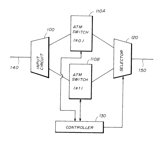
FIG.2 illustrates the entire structure of an
ATM switching system according to the present
2~219368
1 invention. The ATM switching system in FIG.2 includes
an input circuit 100, two ATM switches llOA (#o) and
llOB (#1), a selector 120 and a controller 130. The
input circuit 100 distributes input cells via an input
transmission line 140 to the ATM switches llOA and
llOB. That is, each input cell is supplied to not only
the ATM switch llOA but also the ATM switch llOB. The
ATM switches llOA and llOB have identical structures,
which will be described in detail later. The selector
120 selects either the ATM switch llOA or the ATM
switch llOB in accordance with a switch signal supplied
from the controller 130. The controller 130 manages
the ATM switches llOA and llOB and generates the
above-mentioned switch signal which is supplied to the
selector 120. Output cells selected by the selector
120 are supplied to an output transmission line.
FIG.3 illustrates a detailed structure of a
crosspoint switch provided at a crosspoint in the ATM
switch llOA and a crosspoint switch provided at the
corresponding crosspoint in the ATM switch llOB. A
crosspoint switch llOAl in the ATM switch llOA has a
switch buffer lOa, a cell counter lla, a dummy cell
generator 12a and a difference calculator 13a.
Similarly, a crosspoint switch llOBl in the ATM
switch llOB has a switch buffer lOb, a cell counter
llb, a dummy cell generator 12b and a difference
calculator 13b. A selector 1201 is a part of the
selector 120 shown in FIG.2.
It is now assumed that the ATM switch llOA
(crosspoint switch llOA1) serves as the master and
the ATM switch llOB (crosspoint switch llOBl) is in
the out-of-service state. In this state, the selector
1201 selects cells from the switch buffer lOa of the
crosspoint switch llOAl. The cell counter lla counts
the number of cells in the switch buffer lOa.
Similarly, the cell counter llb counts the number of
cells in the switch buffer lOb. The cell counter lla
2019368
- 13 -
1 of the master crosspoint switch 110A1 indicates the
correct number of cells stored in the switch buffer
10a. On the other hand, the count value in the cell
counter llb of the crosspoint switch 110B1 which is
in the out-of-service state is not identical to that of
the cell counter lla. In this state, according to the
present invention, there are provided three different
change procedures for changing the ATM switch 110B from
the out-of-service state to the slave mode and then
changing the same from the slave mode to the master.
A description will now be given of the first
change procedure. The difference calculator 13b of the
crosspoint switch 110B1 which is now in the
out-of-service state calculates the difference between
the count value in the cell counter lla and the counter
value in the cell counter llb at the commencement of
the first change procedure for changing the ATM switch
110B from the out-of-service state to the slave mode.
It will be noted that the counter value in the cell
counter llb is indefinite. The calculation result,
that is, the difference value, is supplied to the dummy
generator 12b of the crosspoint switch 110Bl through
a line Ll. The dummy cell generator 12b generates a
number of dummy cells which is equal to the difference
value produced and output by the difference calculator
13b. Then, the dummy cell generator 12b supplies the
switch buffer 10b with the dummy cells. It will be
noted that dummy cells are distinguished from other
cells, described below.
As has been described previously, each cell
is comprised of a header and information. The header
includes service bits, which are provided for
indicating the type of cell information being
considered. A dummy cell identification number which
is represented by the combinations of the values of the
service bits and has not yet been used is given to each
dummy cell. The dummy cell can include arbitrary
20~36~
- 14 -
1 information, such as all binary zeros. It will be
noted that the length of each dummy bit should be equal
to that of each cell.
The dummy cells generated and output by the
dummy cell generator 12b are written into the switch
buffer lOb so that the switch buffer lOb has the dummy
cells as well as cells which have been input to the
switch buffer lOb after the ATM switch llOB is switched
to the slave mode. When each of the switch buffers lOa
and lOb has output a number of cells which is equal to
the total number of the dummy cells and the cells which
are already in the switch buffer lob when the dummy
cells are written therein, all the dummy cells have
been discharged so that the switch buffer lOb has cells
which have been input after the dummy cells are written
into the switch buffer lOb. The controller 130 shown
in FIG.2 determines whether or not all the dummy cell
have been discharged from the switch buffer lOb. After
this is confirmed, it is possible to change the ATM
switch llOB from the slave mode to the master mode
since the switch buffers lOa and the switch buffers lOb
arranged at each crosspoint have the same contents
(cells). At this time, the controller 130 sends the
selector 1201 the switch signal so that the selector
1201 selects the cells from the switch buffer lOb of
the crosspoint switch llOB1.
A description will now be given of the second
change procedure. At first, the contents of the cell
counter llb of the crosspoint switch llOB1 are reset
to zero by a reset signal M1, which is supplied from
the controller 130 (FIG.2). This is due to the fact
that the contents of the switch buffer lOb which is in
the out-of-service state are indefinite. Thereby,
binary zeros are written into all the storage areas of
the switch buffer lOb. Next, the counter value in the
cell counter lla of the crosspoint switch llOA1 is
read out therefrom. The readout counter value is
2~19368
- 15 -
1 supplied to the dummy cell generator 12b through a
signal line M2. The dummy cell generator 12b generates
a number of dummy cells which is equal to the counter
value counted and output by the cell counter lla. The
generated dummy cells are then written into the switch
buffer lOb. At this time, the cell counter llb counts
the number of the dummy cells which are written into
the switch buffer lOb. In this state, the controller
130 (FIG.2) controls the crosspoint switch llOBl so
that it operates as the slave switch. Then cells are
output from the switch buffers lOa and lOb. When the
last dummy cell has been output from the switch buffer
lOb, the contents of the switch buffer lOb become
identical to the contents of the switch buffer lOa.
Thus, after that, it is possible to change the ATM
switch lOb from the slave mode to the master mode.
This changing time can be identified by determining
whether or not the number of dummy cells (which is
initially written into the cell counter llb) has been
counted after the ATM switch llOB is changed to the
slave mode.
A description will now be given of the third
change procedure. The first step of the third change
procedure is to read out the counter value in the cell
counter lla of the crosspoint switch llOAl which is
not operating as the master ATM switch. Next, under
the control of the controller 130 (FIG.2), the readout
counter value is preset, through a signal line Nl, in
the cell counter llb of the crosspoint switch llOBl
which is in the out-of-service state. Then, the ATM
switch llOB is changed to the slave mode so that it is
set to the in-service state. The crosspoint switch
llOBl operates as if a number of cells equal to the
counter value written into the cell counter llb is
stored in the switch buffer lOb. Thus, an input cell
which is received after the crosspoint switch llOBl
is changed to the slave mode is written into an area
2019368
- 16 -
1 indicated by the next value of the counter value
written into the cell counter llb. Thus, it becomes
possible to change the ATM switch llOB from the slave
mode to the master mode after the preset number of
cells is output from the switch buffer lOb.
FIG.4 illustrates a more detailed structure
of the crosspoint switch provided at a crosspoint in
the ATM switch llOA and the crosspoint switch provided
at the corresponding crosspoint in the ATM switch llOB
in a case where the ATM switch system is designed to
operate in accordance with the first change procedure.
Referring to FIG.4, a crosspoint switch lllOA in the
ATM switch llOA (FIG.2) is composed of a switch buffer
20a, a cell counter 21a, a dummy cell generator
(marker) 22a and a difference calculator 23a.
Similarly, a crosspoint switch lllOB in the ATM switch
llOB (FIG.2) is composed of a switch buffer 20b, a cell
counter 21b, a dummy cell generator (marker) 22b and a
difference calculator 23b.
The operation of the dual ATM switch
structure shown in FIG.4 will now be described with
reference to FIGS.5A through 5E. It is now assumed
that the ATM switch llOA (crosspoint switch lllOA)
operates in the master mode and the ATM switch llOB
(crosspoint switch lllOB) operates in the slave mode.
In this state, as shown in FIG.5A, both of the switch
buffers 20a and 20b have identical cells ~ - ~, and
the cell counters 21a and 21b indicate identical
counter value "4". It is further assumed that in this
state, the ATM switch llOB in the slave mode is changed
to the out-of-service state due to the occurrence of,
for example, a fault. As is shown in FIG.5B, all the
cells ~ - ~ in the switch buffer 20b are erased.
Even if all the cells in the switch buffer 20b are not
erased, it is impossible to determine what cell is
stored in the switch buffer 20b. Thus, the number of
cells in the switch buffer 20b is indefinite. It will
- 17 -
1 be noted that when the ATM buffer llOB which is in the
state shown in FIG.5B is changed to the slave state,
the contents of the switch buffer 20b are different
from those of the switch buffer 20a.
The ATM switch llOB is changed so that it can
receive cells and outputs cells asynchronously. At
this time, under the control of the controller 130
(FIG.2), the difference calculator 23b calculates the
difference between the counter value in the cell
counter 2la and the counter value in the cell counter
21b, and produces a control signal representative of
the calculated difference. At this time, the
controller 130 (FIG.2) controls the difference
calculator 23a of the master crosspoint switch lllOA so
that it does not operate. The dummy cell generator 22b
generates the number of dummy cells which is equal to
the difference value notified by the difference
calculator 23b, and writes these dummy cells into the
switch buffer 20b. Thereby the counter value in the
cell counter 21b is increased so that the difference
value is added to the number of cells which are already
in the switch buffer 20b when the first dummy cell is
written into the switch buffer 20b. After that, the
counter value in each of the cell counters 21a and 21b
changes each time a cell is written into each of the
switch buffers 20a and 20b or read out therefrom. The
difference calculator 23b always calculates the
difference between the counter values in the cell
counters 2la and 2lb.
The above-mentioned procedure will now be
described with reference to FIGS.5C, 5D and 5E. In
FIG.5C, cell ~ is written into each of the switch
buffers 20a and 20b after the ATM switch llOB is
changed to the slave state from the out-of-service
state. The difference calculator 23b calculates the
difference between the counter values in the cell
counters 22a and 22b in the state where the switch
20~9368
- 18 -
1 buffer 20b has only the cell ~. On the other hand,
six cells ~ - ~ are stored in the switch buffer 20a
and the counter value in the cell counter 2la is equal
to 6. In this state, the difference value is equal to
5. The difference value 5 is written into the cell
counter 2lb so that the counter value in the cell
counter 2lb is changed to 6.
After that, the ATM switch 110B operates in
the slave mode. FIG.5D illustrates a state where four
input cells ~ - ~ have been written into each of the
switch buffers 20a and 20b and four cells have been
output therefrom. It can be seen from the FIG.5D that
two dummy cells are still stored in the switch buffer
20b of the slave crosspoint switch lllOB. In this
state, it is impossible to change the ATM switch 110B
from the slave mode to the master mode. When two cells
have been further output from each of the switch
buffers 20a and 20b, the cells in the crosspoint switch
1110B become identical to those in the crosspoint
switch 1110A, as shown in FIG.5E. That is, the
crosspoint switches 1110A and 1110B are synchronized
with each other. In the above-mentioned manner, it is
possible to change the ATM switch 110A to the master
mode after the number of input cells which is equal to
the counter value in the cell counter 21b obtained when
the number of dummy cells (which corresponds to the
difference value produced and output by the difference
calculator 23b) is written into the switch buffer 20b,
is input to each of the switch buffers 20a and 20b.
FIG.6 illustrated a more detailed structure
of the crosspoint switch arranged at a crosspoint in
the ATM switch 110A and the crosspoint switch at the
corresponding crosspoint in the ATM switch 110B in a
case where the ATM switching system is designed to
operate in accordance with the aforementioned second
change procedure. Referring to FIG.6, a crosspoint
switch 2110A in the ATM switch 110A is composed of a
2019368
-- 19 --
1 switch buffer 30a, a cell counter 31a, a dummy cell
generator (marker) 32a and a difference calculator
33a. Similarly, a crosspoint switch 2110B in the ATM
switch llOb is composed of a switch buffer 30b, a cell
counter 3lb, a dummy cell generator (marker) 32b and a
difference calculator 33b.
The operation of the dual ATM switch
structure shown in FIG.6 will now be described with
reference to FIGS.7A through 7E. It is now assumed
that the ATM switch llOA operates in the master mode
and the ATM switch llOB operates in the slave mode. In
this state, as shown in FIG.7A, both of the switch
buffers 30a and 30b have identical cells ~ - ~, and
the cell counters 31a and 31b indicate identical
counter value "4". It is further assumed that in this
state, the ATM switch llOB in the slave mode is changed
to the out-of-service state due to the occurrence of a
fault, for example. As is shown in FIG.7B, all the
cells ~ - ~ in the switch buffer 30b are erased.
Even if all the cells in the switch buffer 30b are not
erased, it is impossible to determine what cell is
stored in the switch buffer 30b. Thus, the number of
cells in the switch buffer 30b is indefinite. It will
be noted that when the ATM buffer llOB which is in the
state shown in FIG.7B is changed to the slave state,
the contents of the switch buffer 30b are different
from those of the switch buffer 30a.
In this state, the controller 130 (FIG.2)
resets the cell counter 3lb so that the contents
thereof become zero. The difference calculator 33b of
the crosspoint switch 2110B calculates the difference
between the counter values in the cell counters 3la and
31b. The calculated difference value corresponds to
the counter value in the cell counter 3la of the
crosspoint switch 2110A. A control signal
representative of the difference value produced and
output by the difference calculator 33b is sent to the
2019368
- 20 -
1 cell counter 31b and the dummy cell generator 32b.
The dummy cell generator 32b generates a
number of dummy cells which is equal to the difference
value, and writes the dummy cells into the switch
buffer 30b. Each time one dummy cell is written into
the switch buffer 30b, the cell counter 31b is
incremented by +1. Alternatively, it is possible to
write the total number of dummy cells to be written
into the switch buffer 3Ob at one time. In this
manner, the difference value which is equal to the
counter value in the cell counter 3la is written into
the cell counter 31b.
As is shown in FIG.7C, six dummy cells are
written into the switch buffer 3Ob and numeral 6 is
written into the cell counter 3lb when the switch
buffer 30a has six cells ~ - ~ After that, the
crosspoint switch 2110B operates in the slave mode, and
the contents of the switch buffers 30a and 30b and the
cell counters 3la and 3lb change, as shown in FIGS.7D
and 7E. When six cells have been output from each of
the switch buffers 30a and 30b from the state shown in
FIG.7C, all the dummy cells have been output therefrom,
and the contents of the switch buffers 30a and 30b
become identical to each other. After that, it is
possible to change the ATM switch llOB from the slave
mode to the master mode.
FIG.8 illustrates a more detailed structure
of the crosspoint switch arranged at a crosspoint in
the ATM switch llOA and the crosspoint switch at the
corresponding crosspoint in the ATM switch llOB in a
case where the ATM switching system is designed to
operate in accordance with the aforementioned third
change procedure. Referring to FIG.8, a crosspoint
switch 3110A in the ATM switch llOA is composed of a
switch buffer 40a, a cell counter 41a and a difference
calculator 42a. Similarly, a crosspoint switch 3110B
in the ATM switch llOb is composed of a switch buffer
20193~8
-- 21 --
40b, a cell counter 41b and a difference calculator
42b.
The operation of the dual ATM switch
structure shown in FIG.8 will now be described with
reference to FIGS.9A through 9E. It is now assumed
that the ATM switch llOA (crosspoint switch 3110A)
operates in the master mode and the ATM switch llOB
(crosspoint switch 3110B) operates in the slave mode.
In this state, as shown in FIG.9A, both of the switch
buffers 40a and 40b have identical cells (~ 3 and
the cell counters 4la and 4lb indicate identical
counter values "4". It is further assumed that in this
state, the ATM switch llOB in the slave mode is changed
to the out-of-service state due to the occurrence of a
fault, for example. As is shown in FIG.9B, all the
cells(~ ) in the switch buffer 40b are erased.
Even if all the cells in the switch buffer 40b are
erased, it is impossible to determine what cell is
stored in the switch buffer 40b. Thus, the number of
cells in the switch buffer 40b is indefinite. It will
be noted that when the ATM buffer llOB which is in the
state shown in FIG.9B is changed to the slave state,
the contents of the switch buffer 40b are different
from those of the switch buffer 4Oa.
In this state, the controller 130 (FIG.2)
controls the difference calculator 42b so that it
calculates the difference between the counter values in
the cell counters 41a and 41b. The calculated
difference value produced and output by the difference
counter 42b is written, as a preset value, into the
cell counter 41b of the crosspoint switch 3110B.
During this operation, the cell counter is incremented
one by one. It is possible to employ an alternative to
the difference calculation procedure. In the
alternative, the cell counter related to the switch
buffer which is in an out-of-service state (cell
counter 41b in this case) is reset and then the
2019:~68
- 22 -
1 difference calculation is carried out. Then the
difference value thus obtained is written, as a preset
value, into the cell counter 4lb.
In FIG.9C, counter value 6 in the cell
counter 4la representative of the number of cells in
the switch buffer 40a is written into the cell counter
41b irrespective of (that is, by resetting the counter
value) the counter value in the cell counter 4lb. That
is, FIG.9C illustrates the state obtained after a
numeral 6 is preset in the cell counter 41b. After
that, the switch buffer 40b operates in the slave mode,
and the contents of the switch buffers 40a and 40b and
the contents of the cell counters 41a and 41b changes,
as shown in FIGS.9D and 9E. When the number of cells
identical to the preset value has been output from the
switch buffer 40b, the contents of the switch buffer
40b become identical to those of the switch buffer
40a. Thus, it becomes possible to change the ATM
switch llOB from the slave mode to the master mode.
Each of the aforementioned switch buffers can
be formed of an elastic memory. As is well known, a
write reset signal and a read reset signal are supplied
to the elastic memory. Data is written into the
elastic memory in synchronism with a write clock, and
data is read out therefrom in synchronism with a read
clock. It is possible to determine how many cells have
been written into the elastic memory after the write
reset signal is applied thereto. It is also possible
to determine how many cells have been read out from the
elastic memory after the read reset signal is applied
thereto. Each of the aforementioned cell counter is
supplied with these clock signals and determines the
number of cells which are stored in the related switch
buffer by calculating the difference between the number
of write clocks and the number of read clocks.
The present invention is not limited to the
specifically disclosed embodiments, and variations and
20l936~
- 23 -
1 modifications may be made without departing from the
scope of the present invention.