Note: Descriptions are shown in the official language in which they were submitted.
~ }2~
Di~ning method and de~ice for 1uorescent lamp8
used for backlighting of liquid crystal screens.
BACKGROUND OF THE INVENTION
This invention relates to a dimming method and devlce for
fluorescent iamps to be used in a backlighting system for liquid
crystal visual displays.
Liquid crystal screens, more particularly those used for
5 colour visual display on instrument panels in aeroplanes and
helicopters, are equipped with backlighting systems which pro-
vide a high level of brightness making them comfortably visible
even with strong ambient light. This brightness must be variable
allowing it to be adapted to the various intensities of ambient
l0 light, and this brightness must also be adaptable to day-night
ambient variatlons. Such variations imply a light dimming ratio
of 1000:1, whlch for fluorescent lamps correspond~ to a bright-
ne~s intensity of a few Cd/m2 for minimum brlghtness and
approximately 15,000 Cd/m2 for maximum brightness.
It ls to be noted that the light source uses fluorescent
lamps due to their high energy efficiency and to their colorime-
try which is well-adapted to liquid crystal screens.
To obtain an optimal brightness level with these lamps,
the power supply voltage which is applied between their two
electrodes is a high alternating voltage, generally between 300
20 and 500 volts, at a frequency of several tens of kilohert~.
As is well-known in the art, it ls possible to vary the
brightness of a fluorescent lanip by varying the amplitude of the
power voltage and consequently, the current traversing the
lamp. This method is only capable of producing a brightness
25 dimming ratio of 10:1, which is insufficient for the above-men-
tioned application. Moreover, the fact that the triggering volt-
age of a fluorescent lamp is dependent on the temperature, more
precisely, that this voltage increases as temperature falls,
~2~ $
implies that thls brightness control method does not a110w opera-
tion over a wide temperature range, especially when the tempera-
ture is below 0C.
It is generally known that the range of brlghtness levels
can be improved by modulating the frequency oî the alternating
supply voltage and, more precisely, by using, for example,
square waves of frequency varying from tens of hertz to tens of
kilohertz. In this case, however, to satisfy the aforementioned
conditions of operation, it is necessary to work with frequen-
0 cies of less than 15 kilohertz in order to produce low bright-
ness levels and at these frequencies sound vibrations may re-
sult. Finally, at a very low brightness level there appears a
flickering due to stroboscopic effect between the intermittent
ignition of lamps and the refreshing of the image of which the
frequency is between 50 and 60 hertz. This results in a bright
horizontal bar on the screen which is absolutely unacceptable
for pilot control displays.
As is also well-known in the art, the brightness of a
fluorescent lamp can be varied by applying a square wave volt-
age with an ad~ustable duty cycle width. However, there exist
problems with respect to stroboscopic effect in this method too.
SUMMARY OF THE INVENTION
The purpose of the present invention is to resolve such
problem~. The solution is provlded by a pulsed supply voltage
to a fluorescent lamp used for the backlighting of a liquid
crystal screen. The width of the bursts can be altered accord-
ing to the required level of brightness. The start of the
bursts i8 synchronized with the "image synchronizing" signal of
the liquid crystal screen.
According to the present invention, there is provided a
dimming method for fluorescent lamp used for the backlighting of
a liquid crystal screen with an image ~ynchronizing signal asso-
ciated to the screen, the method consisting in applying an
2 ~
alternative supply voltage to the lamp, switching the alterna-
- tive supply voltage by means of rectangular periodic slgnals
having ad3ustable duty cycles which depend on the luminous
intensity required for the lamp and in synchronizing the rectan-
5 gular signals with a signal corresponding to the image synchroni-
zing signal divided in frequency by a whole number, n, supe-
rior to 0.
According to the present invention there is further provi-
ded a dimming device for fluorescent lamp used for the backlight-
10 ing of a iiquid cry~tal screen wlth an image synchronizing sig-
nal associated to the screen, comprising: a switching genera-
tor producing switching signals at a fixed frequency in form of
rectangular periodic signals made of pulses with adjustable
width; synchronizing means for synchronizing the switching
15 signal wlth a signal corresponding to the image synchronizing
slgnal divlded by an integer greater than 0; an alternative
voltage generator to provide power to the fluorescent lamp; and
locking mean~ controlled by the switching signals to aliow the
voltage generator to functlon only during the duration of the
20 pulses of the rectangular periodlc signal~.
BRI$F DESCRIPTION OF THE DRAWINGS
For an improved understanding and illustration of the
characteristics of the invention the following diagrams are
presented:
25 - Figure 1 i8 a circuit diagram representing a dimming device,
according to the invention, for a fluorescent lamp used for the
backlighting of a liquid crystal screen;
- Figure a 1~ a timing diagram to explain the operation of the
device illustrated in Figure 1; and
30 _ l~igure 3, a partial circuit dlagram representing B variant
embodiment of the device illustrated in Flgure 1.
DETAILED I)ESCRIPTION O~ THE PREFERRED EMBODIMENTS
12~ 2$
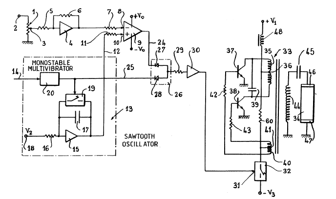
Eigure 1 illustrates a brightness control potentiometer 1
- which receives negatlve DC supply voltage at a terminal 2. Part
of this direct voltage is tapped by a slider 3 of the potentiome-
ter 1, in order to provide a direct voltage, which i9 ad~usted
5 by means of the slider 3, which after amplification by the opera-
tional amplifier 4 (combined with a series reslstance 5 and a
negative feedback resistance 6) is applied via resistance 7 to
the input inverter 8 of a voltage comparator 9, which is fed by
a DC voltage ( l Vo, -Vo) .
l The non-inverting input 10 of the comparator is connect-
ed, via a resistance 11, to the output 12 of a sawtooth oscilla-
tor 13, whose signals are synchronized with the image synchroni-
zing pulse signal of a liquid crystal screen; this pulse signal
i8 applied to 14 on the oscillator 13.
This oscillator 13 comprises an operational amplifier 15
mounted as an integrator using a capacitor 17 connecting input
and output, and a resistance 16 whlch connects its input to a
terminnl 18 to which i8 applied a reference voltage V2.
Rapld return of sawtooth pulses i~ provided by means of
20 ~ rapid CMOS-type analog swltch 19 connected in parallel with
the capacitor 17 and which is controlled by image synchronizing
pulses produced by a monostable multlvibrator 20.
In Figure 2, a diagram showing curves amplitude (A)
versus time (t), the (negative) image synchronizing pulses 21
25 are represented on the upper curve A, whereas sawtooth pulses
at output 12 of oscillator 13 are represented on curve B. The
ad~ustable direct voltage applied to 8 is represented by the
broken dash-dot line at 22.
As long as curves B and 22 intersect, the intermittent
30 negative voltage bursts 23, of the duty cycle L, ad~ustable by
means of the slider 3, are generated at output 24 of the compara-
tor 9, the amplitude of these bursts being equal to Vo.
The elements with reference numbers 1 to 20 form an
intermittent pulse generator with fixed frequency and an ad~ust-
35 able duty cycle whereby the bursts are synchronlzed with the
;2~ $```~
image synchronizing pulses 21 of the llquid crystal screen requi-
ring backlighting.
The output 24 of the comparator 9 provides rectangular
signals 23 made of pulses and the output 25 of the monostable
multivibrator 20 provides pulses 21; these outputs are respec-
tively connected to two diodes 27, 22 of an OR circuit 26; the
output of circuit 26 is coupled, via resistance 29, followed by
a regenerating amplifier 30, to the control input 31 of a differ-
ent analog switch 32. This switch 32 is open when a negative
pulse 23 or 21 is applied to 31, and it is closed in the oppo-
site case. It acts as a control switch for the high alternating
voltage supply oscillator 33 to the fluorescent lamp 34.
The oscillator 33 comprises: a transformer with a main
primary winding 35 and a center tap 36, a feedback winding 40
and a center tap 41, and a secondary winding 44, two N-P-N
transistors 37, 38, a capacitor 39, three resistances 42, 43, 60
and an induction coil, 48. The emitters of transistors 37, 38
are connected to ground, and their collectors are connected
respectively to the two extremities of the primary winding 35,
and the bases are connected respectively to the two extremities
of the feedback winding 40. The capacitor 39 is situated between
the two extremities of the primary winding 35. The secondary
hlgh-voltage winding 44 of the transformer has one terminal
grounded and another terminal connected, via a ballast capscitor
45, to an electrode 46 of the fluorescent lamp 34; the other
electrode, 47, is grounded.
The positive supply voltage l V1 from the oscillator 33 is
applied via the induction coil 48, to the center tap 36 and then
across the resistance 60, to the center tap 41, while a negative
30 direct control voltage -V3 is applied when the switch 32 is
closed, to the center tap 41, then across the resistance 60 to
the center tap 36.
Circuit operation in Figure 1 is the following:
When the slider 3 of the potentiometer 1 is at the upper
35 limit (in ~igure 1~, the positive voltage applied to the termi-
2~
nal ~ ls maximum, greater than that of the sawtooth B, so that adirect voltage level equal to -Vo is applied to 24.
The voltage applied to the control lnput 31 of the switch
32 is then continuous, so that the switch 32 remains open perma-
5 nently and the oscillator 33 operates without interruptlon,allowing the fluorescent lamp 34 to operate at a level of maxi-
mum brightness.
When the slider is progressively moved downwards from
this upper limit (approaching ground state), the voltage 22
10 (Figure 2) decreases in amplitude and intersects the sawtooth
curve B which generates pulses 23, with a duty cycle L, which
progressively decrease as the slider 3 approaches ground state,
and for which the leading edge is synchronized with that of the
pulses 21. The oscillator 33, at this point, operates only dur-
5 ing the pulses 23 (curve D in Figure 2) since during the pulse-
free period the switch 32 is closed and the voltage -V3 conse-
quently blocks the oscillator 33.
The brlghtness level obtained by the lamp 34 is therefore
proportional to the duty cycle L of the pulses 23, which depend
20 on the position of the slider 3.
When the slider 3 reaches its lowest limit (ground side),
no signals appear at output 24, however, due to the OR circuit
28, pulses 21 are nevertheless applied to the control terminal
31, whlch causes the oscillator 33 to function while the image
25 synchronizing pulses 21 are present: in this manner a minimum
visible brightness level is obtained for the lamp 34.
The clrcuit according to Figure 3 represents another
version according to the invention, where the differences with
respect to Figure 1 have been illustrated; thls circuit compris-
30 es a series resistance 49, or "foot resistance" whlch Is placed
between the electrode 47 of the lamp 34 and the ground. Theterminal voltage of this resistance 49 Is applied, via a rectifi-
er 50 and a series resistance 51, to a first input 52 of a dif-
ferential amplifier 53. The other input 55 of this differential
7 ~9'~
amplifler 53 receives by means of a reference voltage V4 and an
ad~ustable resistance 54, a direct ad~ustable voltage.
The output of the differential amplifier 53 is connected
to the control input 56 of a voltage regulator 57 which is inser-
5 ted between the power supply terminal ~V1 and the inductioncoil 48 and whlch is capable of varying the direct voltage at
its output 58 in relation to the control voltage which lt re-
ceives at input 56.
The part of the devlce in Figure 3 corresponding to refer-
10 ence numbers 49 to 57 forms a control loop wlth the rôle ofreguiating the current in the re~istance 49 and at the same
time, in iamp 34J to the value indlcated by the reference volt-
age applied to input 55, this value depending on that of the
ad~ustable resi~tance 54; thusJ lt 18 possible to optimize the
15 value of supply voltage to the lamp 34 with respect to its work-
ing pointJ by minimizing the power loss and by freeing itself of
temperature variations.
MoreoverJ the circuit illustrated in Flgure 3 provides
for the trlggerlng oP the lamp 34 at a low brlghtne~s level or
20 at a very low amblent temperature.
In relatlon to this sub~ect, it is recalled that the
trlggerlng voltage oP fluorescent lamps depends on the tempera-
ture oP the electrodes and of the tube retaining the mercury
vapour. At a low level of brlghtness, the mean current travers-
25 ing the iamp 1~ very weak and does not heat the lamp. Thetrlggering voltage is therefore higher than when the level of
brightnes~ of the lamp is higher. The trlggerlng vdtage also
increases when the amblent temperature decreases.
Should trlggering not occur, due to an Insufflcient level
30 of brlghtness or low amblent temperature, no voltage ls applied
to terminal 52 of the differential amplifler 53, so that the
maximum control voltage of regulator 57 Is applied to 53, thus
increasing the effectlve supply voltage of the oscillator 33 to
over its trlggering voltage ln such unfavourable condltlons,
8 2 0 ~
which oP course supposes that the vdtage l V1 i9 of sufficient
amplitude .
The circuit in Figure 3 allows for pairing of lamps of
low luminosity.
In the case of a lighting system with two or more fluores-
cent lamps, it is necessary to pair lamps for low brightness
levels in order to obtain identical triggering voltages for the
lamps, otherwise, one of the lamps is likely to light up and not
the other. For this purpose, each lamp has its own circuit
according to ~igure 3. This matching is carried out by ad~usting
the resistances 54 of each circuit so that all the lamps start
under the same operational conditlons. To achieve the same re-
sults it ls also possible to ad~ust the foot resistances 49, but
this solution is not as good as there is the risk of increasing
i 5 losses .
It has been explained previously that a minimum level of
brightness l~ obtained by chopping or modulating the alternating
voltage of oscillator 33 by means of pulses which last for a
period of time equivalent to the duty cycle of the image ~ynchro-
nizing pulses 21. In fact, these pul~3e~ 21 have a duty cycle of
about 50 microseconds. Theoretically, to obtain, as required, a
varlation of luminosity in the fluorescent tube 34 of 1 to 1000,
the duty cycle L of puises 23 must range from 5() microseconds
to 1000 times more, in other words 50 milliseconds. Whereas,
chopping to 50 milliseconds corresponds to a frequency of 20
hertz, and this would Introduce a flicker effect in the image
produced on the liquid crystal screen which means that if this
theory is purely and simply followed, this devlce according to
the invention will not operate in the required conditions (dim-
ming ratio of 1000:1).
In reality, this is not the case because when the lamp 34
is only allowed to operate during 50 microseconds, it does not
have sufficient time to heat up, and the trigering operation in
itself is not sufficient to increase the temperature of the
lamp. Therefore the brightness efficiency of the lamp when cold
2 ~
is three times inferior to that during continuous or nearly
continuous operation, in other words when hot, 80 that the
brightness ratio of 1 to 1000 is finally obtained by passing,
for the burst duty cycle L of the sinu~oidal alternation of the
5 oscillator 33, from 50 microseconds to around 1~ milliseconds,
which correspond~ to a chopping frequency far higher than
those which cause flickering.
The invention is not limited to the embodiments described
above. It is thus possible, for example, in the case of automat-
l 0 ic regulation of the surrounding light level to replace thebrightness control potentiometer 1, with a photodetector which
supplies a voltage proportional to the required brightness. In
the above example, the beginning of each pulse 23 of the sinu-
soidal alternation of the oscillator 33 is synchronized With the
l 5 image synchronizing signal of the liquid crystal screen . In
order to extend the operational dynamics of the device it is
also possible to synchronize this pulse using the image synchro-
nizing signal divided in frequency by an integer greater than 1.
It is obvious that this is only possible if the frequency of the
20 signal divided by this number is not too low, in which case a
fllekering effect will result. It is also possible, when several
fluoreseent lamps are required, to use only one switch 32, given
that a re~istance is inserted in connection between this switch
and the center tap 41 of each oscillator related to each lamp.