Note: Descriptions are shown in the official language in which they were submitted.
202027S
Attorney Docket No. 10577-173-F
APPARATUS AND METHOD FOR READING, WRITING,
AND REFRESHING MEMORY WITH DIRECT VIRTUAL
OR PHYSICAL ACCESS
FIELD OF THE INVENTION
This invention relates to a computer memory and a
method for reading, writing, and refreshing the contents of
the memory. In particular, the invention relates to a rapid
method for virtual addressing of a fast page dynamic random
access memory (FPDRAM).
BACKGROUND
There has been, for some time, a trend toward
larger memory capacity in computers. Although larger memory
capacities provide a number of well known advantages,
several difficulties are also encountered with large memory
systems. In general, as memory size increases, the time
needed to access memory also increases, other factors
remalning equal.
In many modern computing systems, the memory is
provided in a hierarchical scheme. In such a scheme, a
large, relatively slow memory is used in combination with a
smaller, faster memory, which contains a subset of the
larger memory. For example, a main memory containing
relatively slow dynamic random access memory (DRAM) is used
in combination with a smaller static random access memory
(SRAM), often referred to as a "cache." Other hierarchies
include providing a large memory, in the form of relatively
'\C
- 202û27~
slow disk storage, used in combination with the relatively
faster DRAM main memory. A memory hierarchy might contain
all three of these levels: long-term disk storage, main
DRAM storage, and SRAM cache storage.
In many memory systems, a virtual addressing
method is used. The virtual address is an address which
contains enough bits to provide a unique identification for
each user-accessible memory location. Physical memory is
accessed through a physical address which must be mapped-to
from the virtual address space.
When a request is made for the contents of memory
identified by its virtual address, it must be determined
whether the virtual address corresponds to a memory location
currently residing in the physical memory. An address
"corresponds" to another address if each corresponds to the
same memory location.
One or more tables are usually provided to
translate a virtual address to a corresponding physical
address (if there is a correspondence). A look-up procedure
for such a table is often relatively slow. The table
typically contains a translation only of blocks of memory,
often referred to as "pages." Fortunately, it has been
found that references to the page table exhibit a locality,
i.e., of all the possible virtual pages that might need to
be looked up in the page table, during any one short period
of time, there is a tendency for a few of these pages to be
repeatedly looked up. This locality permits a certain
saving of time by providing a second smaller and faster
- 2020~75
table, referred to as a "page table cache" (PTC) (or,
sometimes, a "translation lookaside buffer"), which is used
to contain the most recently accessed entries from the
larger page table. The PTC thus contains a subset of the
page table which is likely to contain the entries which will
be subsequently requested. The PTC includes two arrays.
one array is the PTC entry or data array, which is the
virtual-to-physical address map. The other array is the PTC
tag, which is used to determine whether or not the data in
the PTC entry is valid.
In addition to the locality exhibited by the page
table, a certain locality is also exhibited by the memory
itself. According to this locality phenomenon, a given
reference to a memory location is likely (i.e., with greater
probability than expected from randomness) to be followed,
within a relatively short period of time, by a request for a
nearby memory location. The probability distributions,
which define "nearby" and "relatively short period of time,"
can be determined empirically for a given memory system and
computing task. This locality has been exploited in several
ways to decrease average memory access time. One method of
this exploitation is the provision of a fast page dynamic
random access memory (FPDRAM).
FPDRAM can be best understood by contrasting it
with ordinary memory access. In a typical DRAM, memory
locations are addressed by row and column, with each row
containing elements with contiguous addresses. In normal
access, a row address is presented and strobed into a latch
4 20202~5
with a row address strobe (RAS), which is typically
asserted. Later, a column address strobe (CAS) is presented
and asserted to perform the read or write of the DRAM. Each
new access must go through the entire cycle. For this
reason, each access requires presenting and strobing the row
address and, subsequently, strobing a column address.
Because two addresses, even if relatively close together,
must be sequentially strobed for any access in the memory,
this type of access does not take full advantage of the
memory locality.
In contrast, FPDRAM takes advantage of memory
locality, i.e., situations in which access to a memory
location in a particular row is relatively likely to be
followed, within a short time, by a request for a memory
location in the same row. In this case, it is possible to
leave RAS asserted for a relatively long period, during
which multiple accesses to the selected row (defined by the
contents of a row address latch) may be performed. The
multiple accesses are achieved by sequentially presenting
column addresses while a single row address is continuously
asserted. For each access to memory in a row which has been
previously accessed (i.e., a row addressed by the contents
of one of the row address latches), only assertion of CAS is
required, i.e., it is not necessary to sequentially assert
RAS and then assert CAS for each access. In this way, when
a subsequent memory request is made for a location in the
same row, this subsequent address is available for reading
or writing by the relatively fast procedure of presenting a
- 202027s
new column address and asserting the column address strobe
(CAS). When a request is made for a memory location in
another row (assuming there are no other FPDRAM row address
latches usable for this request), a normal access procedure
is followed, i.e., sequential loading and strobing of a row
address, then a column address. In this way, to the extent
that subsequent memory accesses are to locations in the same
row of memory, relatively fast FPDRAM memory access is used,
rather than the slower normal memory access.
To take advantage of the speed of an FPDRAM, it is
necessary to determine, for any memory request, whether that
request is for a memory element which resides in one of the
rows corresponding to a row address in one of the row
address latches. In previous systems known to the
Applicant, an indication of the physical row address for the
row or rows most recently accessed was stored. When a
physical address request was made, a comparison was
performed to determine whether the requested address was in
a row recently addressed, i.e., for which the RAS was still
being asserted. When a virtual address request was made,
the virtual address was first translated into a physical
address, and then the comparison was made with the stored
physical addresses.
Even with the relatively fast access provided by
FPDRAM, memory access is still a limiting factor in many
systems, particularly those with large memories. Such large
memory systems typically are limited by the speed of a
cache-fill operation and the write bandwidth.
- 2020275
.~UMMARY OF THE INVENTION
The present lnventlon lncludes a computer memory and
a method of memory access which provides for faster memory
access, compared to previous systems, particularly for
configurations with very large memories, such as 128 megabytes
or more of memory. The present inventlon can be used ln
connectlon wlth any type of random access memory (RAM) in
which access time to some subset of the RAM elements is faster
than to other elements. FPDRAM's are one example of memories
of this type, slnce access to elements in a currently selected
row is faster than access to other elements.
Broadly, the lnventlon ls directed to a computer
memory system capable of recelving a plurality of virtual or
physical address requests. The invention includes a row and
column addressable random access memory having at least one
row address latch capable of indicating a plurallty of memory
locatlons, all of which have a common physlcal row address; a
flrst reglster for storing portions of a row address
corresponding to the physical row address during a first and
second of the plurallty of address requests, wherein the
contents of the flrst reglster comprlses at least portions of
a virtual address during a flrst tlme period and at least
portions of a physical address, different from the virtual
address, durlng a second time period, the second time period
being different frorn the first time period. A comparator
receives at least a portion of an address request, whether a
physical address request or a virtual address request, for
comparison to portions of the flrst reglster to determlne
, _A 64157 331
- 2020275
whether the rnemory location indicated by the address request
ls lncluded ln the plurallty of memory locatlons.
The method of accesslng a memory, accordlng to the
~ present lnventlon, broadly lnvolves the steps of provldlng a
fast page dynarnlc random access memory array havlng at least
one row address; provlding at least a flrst vlrtual~physlcal
address reglster for holding at least a portlon of a row
address correspondlng to a row held by at least a flrst row
address latch whereln the contents of the flrst vlrtual/
physlcal address register comprises at least portlons of a
vlrtual address durlng a flrst tlrne perlod and at least
portlons of a physlcal address, dlfferent from the vlrtual
address, durlng a second tlme perlod, the second tlme perlod
that ls dlfferent from the flrst tlme perlod; comparlng
selected blts from a memory request address, whlch may be a
physlcal address request or a vlrtual address request, wlth
the contents of the vlrtual/physlcal address reglster to
generate a flrst slgnal when the selected blts are ldentlcal,
and to generate a second slgnal when the selected blts are not
ldentlcal; and assertlng a column address strobe to the row
address latch followlng the first slgnal.
In one embodlment of the present lnventlon, one or
more FPDRAM's form the maln memory, frorn whlch requested pages
are loaded lnto a cache. As descrlbed more fully below, pages
are requested from a partlcular FPDRAM only after lt has been
determined that the address mapped by the PTC ls the memory
locatlon whlch was requested, by looklng up the address ln the
PTC tag.
6a
- 64157-331
2020275
Each row address latch of the FPDRAM is associated
with two reglsters. One "indicator" register (termed the
"CAMPhyAdr") contains the physical row address (plus
addltional bits, such as parlty bits). The other
"virtual/physical" register (termed the "CAMTag") contains
either the physical row address or the virtual row address,
depending on which type of address was originally requested.
In this way, when a virtual address is requested (after
6b
64157-331
7 202027~
verifying its presence in the PTC tag array), it can be
compared to the virtual/physical (CAMTag) register without
the necessity for first translating to obtain the physical
address. The system described thus provides for rapid
memory access in the case of virtual address requests, which
are the most common mode of address requests. The system
also provides for memory access resulting from physical
address requests using the same methods as those for virtual
address requests. The described methods work particularly
well because memory requests in most situations have been
found to exhibit a virtual/physical "locality," i.e.,
repeated requests from the same row tend to be of the same
type, either virtual or physical. Avoiding the necessity of
the virtual-to-physical translation to determine, in each
case, whether the address being selected is in a row
addressed by contents of a row address latch, represents a
valuable savings of time. Because virtual-to-physical
translation is not needed for each memory access, such
translation can be done with slower, less expensive
components, e.g., a slower page table cache, while still
achieving rapid memory read and write.
When no match is found to the requested row, the
row needed is accessed by the slower normal access mode.
When a memory element in a new row is to be accessed, it is
necessary to determine whether the memory request was a
virtual address or a physical address. For this reason, a
bit which indicates whether that address is virtual or
8 202027S
physical is stored in the CAMTag register, along with the
virtual or physical address.
An additional aspect of the invention relates to
accommodating the width of an address. The width needed to
uniquely address elements in a block of memory depends on
the size of the block. In the preferred embodiment of the
present invention, the DRAM's which are used require 10
column address bits and 10 row address bits. The virtual
address in this system contains page address bits and word
address bits. The word address bits are identical in the
virtual and physical addresses, and thus the word address
bits are not translated. The number of word address bits in
a virtual address is determined by the number of words in a
page. In the preferred embodiment, the page size is 2 k
bytes or 1 k 16-bit words. A page of this size can be
addressed using 10 bits, and thus the virtual address
contains ten word address bits. This means that 10 bits in
the virtual address are identical to the corresponding bits
of the physical address.
The DRAMs which make up the memory are organized
in a four-way interleaved fashion, i.e., four consecutive
words in memory come from four different DRAMs, rather than
four cells in the same DRAM. In this scheme, during a read
operation, the two least significant bits of the 10-bit word
address are used to select between the four interleaved
words. Thus, the two least significant bits of the word
address are not used in a read operation, and are discarded
(for purposes of DRAM-addressing). Thus, eight word address
9 2020275
bits (which do not require any translation) remain for use
as column address bits. Since the DRAMs require 10 column
address bits, two column address bits must come from the
part of the physical address which does require translation.
Yet, it is desirable to eliminate the need for translation
on repeat accesses to the same page of lK words. This is
accomplished by storing the required additional two bits of
column address in the CAMPhyAdr register, along with the 10
bits of row address (and also including parity or other
error detection bits, bank-select bits, and/or board-select
bits). Because only eight bits of word address contribute
to the 10-bit column address, two column address bits of the
address space do not change between misses.
Storage of two column address bits is similarly
employed for addressing DRAM in a write operation. In the
preferred embodiment, however, only one or two words are
written in a single write operation. To prevent overwriting
of unaddressed words, the two bits which would be discarded
on a read operation are used to select which one or two
words, among the four potentially addressable, will have a
column address asserted, to accomplish a write at that
location.
Storage of column address bits for use during CAM
hit accesses is an accommodation that can be generalized for
use with different types of memory. For example, three or
more bits can be stored in the indicator (CAMPhyAdr)
register to provide a total of 11 or more column address
bits. Provision of 11 column and row bits would be useful,
2020275
e.g., in connection with a 4 megabit DRAM, which typically
requires 11 column address bits and 11 row address bits to
access a memory element. Storage of more than two column
address bits can also be useful to provide additional least
significant bits for selecting among interleaved DRAMs in
the case of, e.g., eight-way interleaving.
The present system achieves a decreased cache fill
time and an increased effective write bandwidth, compared to
previous systems not employing the disclosed invention.
The present invention includes a refresh cycle for
the DRAM, which is efficient because the contents of the
associated CAMTag register and CAMPhyAdr register are
preserved. The RAS is deasserted during the DRAM refresh.
Following the refresh, the RAS is reasserted, in a manner
similar to RAS assertion following a CAM miss (i.e., non-
identity of the contents of the CAMTag and corresponding
portions of the requested addresses). In this way, the
memory configuration following the refresh cycle is the same
as it was before the refresh cycle. Thus, subsequent memory
accesses can be accomplished taking advantage of the memory
locality, based on row accesses which were performed before
the refresh cycle.
BRIEF DESCRIPTION OF THE DRAWINGS
Figs. lA-H are simplified schematic diagrams of
the memory system of the present invention;
2020275
11
Fig. 2 is a schematic block diagram of the memory
system of the present invention showing data paths, but not
control paths;
Fig. 3 is a flow diagram of a memory-read
operation with a CAM hit according to the present invention;
Fig. 4 is a flow diagram of a memory-write
operation, with a CAM hit according to the present
invention;
Fig. 5 is a flow diagram of a memory-read
operation with a CAM miss according to the present
inventlon;
Fig. 6 is a flow diagram of a DRAM refresh cycle
according to the present invention;
Fig. 7 is a state diagram of the MEMOP state
15 machine;
Fig. 8 is a state diagram for the receive state
machine;
Fig. 9 is a state diagram of the refresh state
machine;
Fig. 10A is a schematic diagram of a virtual
address;
Fig. 10B is a schematic diagram of a physical
address;
Fig. 10C is a schematic diagram of an address used
25 by RAM;
Fig. llA depicts the bit types stored in the
CAMTag registers;
12 2020~75
Fig. llB depicts the bit types stored in the
CAMPhyAdr registers; and
Fig. 12 is a schematic block diagram of a PTC with
distributed entry and tag arrays.
DETAILED DESCRIPTION OF THE PREFERRED EMBODIMENT
The preferred embodiment of the present invention
will be described in the context of a particular computing
system, although, as will be apparent to those skilled in
the art, it can be used in many types of computing systems.
The described computing system is a multi-processor system
containing up to 16 processors, each processor having
associated with it a memory system. In the preferred
embodiment, the memory system associated with each processor
includes two functional units 93a (Fig. 2). Preferably,
each functional unit is formed on one or two circuit boards,
each circuit board containing 32 or, preferably, 64
megabytes of memory, along with memory control devices. The
present invention relates to a memory unit associated with
one of such processors. Each of the memory units in the
computing system operates in substantially the same way.
Fig. 10A depicts the configuration of a virtual
address which includes a segment address 2 in bits 0-14, a
page address 4 in bits 15-20, and a word address 5 in bits
21-30. Fig. 10B depicts the configuration of a physical
address in which the physical page address 6 is contained in
bits 0-20, and the word address 5 is contained in bits 21-
30.
13 2020275
Referring now to Fig. lOC, an address as used to
access the DRAM is depicted which is 30-bits wide. The
address includes 10 bits of column address and 10 bits of
row address. The row address is provided in bits 7-16 (12,
14). The column address is provided in bits 17 and 18 (16)
and bits 21-28 (20). Bits 1-5 (22) indicate which memory
board is addressed. Bit 6 (24) indicates which section of
memory ("X" or "Y") is addressed. Bits 19 and 20 (26) are
bank-select bits. Bits 29 and 30 (28) are used in the
pseudo-interleave scheme.
Before describing in detail the operation of the
preferred embodiment of the invention, the main concepts of
the invention will be described by way of a simplified
example with reference to Figs. lA-lE. A simplified memory
unit, depicted in Fig. lA-lE, includes a 64-element memory
10 having eight rows, la-lh, and eight columns, 2a-2h. The
memory is of a fast-page type in which the row selector 3
can be left to select a given row, according to the address
in a row address latch 4, during a number of successive
column addresses by the column selector 5. Associated with
the memory 10 are two registers, a CAMPhyAdr register 6,
which holds a physical address, and a CAMTag 7, which holds
an address that may be either a physical address or a
virtual address. For purposes of the simplified
explanation, it is assumed that an address request 8 has
just arrived. The address request 8 can be an address to be
used for either a read or a write to the memory. In a
typical scenario, such an address request arrives after a
processor has made an attempt to read or write to a cache,
- 202027~
14
which was unsuccessful because the required address was not
present in the cache. In case of such a "cache miss,"
memory must be fetched from the main memory 10 for transfer
to the cache.
It is assumed in the present example that the
previous access to the memory left the memory unit in the
configuration shown in Fig. lA, i.e., with the eighth row,
row 111, selected. Accordingly, the row address latch 4
contains row address bits 111, and the CAMPhyAdr 6 contains
the same row address (111). It is further assumed that a
previous address request was for a virtual address.
Accordingly, the CAMTag 7, as shown in Fig. lA, contains a
row address which is left over from the previous address
request, and is thus the virtual address corresponding to
the physical address 111. As seen from the page table 9,
the virtual address which corresponds to the physical
address 111 is 101.
As can be seen from Fig. lA, the new address
request is of the form 001110. To process the new request,
first a comparison is made between the row bits in the
address request 8 and the contents of the CAMTag 7. In this
case, the row bits in the address request 8 are 001, while
the contents of the CAMTag 7 are 101 (left over from the
previous memory request). Accordingly, the comparator 11
indicates that there is a CAM miss. This means that the
newly-arrived address request 8 is for a row different from
the row which is presently asserted (i.e., different from
row 111).
- 2020275
When the comparator 11 indicates a miss, the
registers 6, 7 are updated, as depicted in Fig. lB. The
CAMTag 7 is loaded with the row address from the address
request (i.e., 001). In a case in which the new address
request is a physical address, the row bits of the physical
address can be transmitted directly to the CAMPhyAdr 6. In
such a case, the CAMTag and the CAMPhyAdr will contain
identical indications of the requested row. As used herein,
a bit string "indicates" an address or a memory location if
at least a portion includes or can be translated into an
address corresponding to the memory location.
In the present example, however, it is assumed
that the address request 8 is a virtual address, thus
requiring translation. The page table 9 is used to
determine which physical address corresponds to a virtual
address of 001. The page table 9 indicates that the
corresponding physical address is 010. As shown in Fig. lB,
this new physical address is loaded into the CAMPhyAdr 6.
As can be seen from Fig. lB, the CAMTag 7 now contains the
virtual row address for the new request, while the CAMPhyAdr
6 contains the corresponding physical row address. The
physical row address from the CAMPhyAdr 6 is sent to the row
address latch 4, causing the row selector 3 to select the
row addressed by the physical row address, namely, row 010.
As depicted in Fig. lC, the address request 8 is
now attempted again, using the new contents of the CAMTag 7
and CAMPhyAdr 6. This time, when the row bits of the
address request 8 are compared to the contents of the CAMTag
7, the comparator 11 indicates a hit. The column selector 5
20~0~75
16
selects a column in accordance with the column bits from the
address request 8.
Fig. lD depicts the next successive address
request, which is, in this example, 001000. The row bits
from the address request 8 match the contents of the CAMTag
7. Accordingly, the virtual row address of the new request
8 is identical to the virtual row address from the previous
request, which was depicted in Fig. lC. As a consequence,
the row selector 3 is still configured to select the third
row, 010. Because there has been a hit indicated by the
comparator 11, the column bits from the address request 8
(i.e., 000) are used, by the column selector 5, to select
the column 000.
Figs. lE-lG depict a simplified version of an
embodiment of the invention which can be used when not all
of the column bits can be directly used to control the
column selector 5. In the embodiment depicted in Figs. lE-
lG, the third column bit is stored in the CAMPhyAdr, along
with the physical row bits, and is also stored in the CAMTag
7, along with the virtual or physical row bits. It can thus
be seen that in the embodiment depicted in Figs. lE-lG, the
third column bit is treated, in many respects, as if it were
an additional row bit. It is stored in the CAMPhyAdr, along
with the physical row bits, and a previously stored third
column bit (left over from the previous memory access) is
compared to the new third column bit in the incoming address
request 8. By storing the third column bit and combining it
with the first two column bits from the address request 8,
as described below, the third column bit in the address
17 2020275
request 8 is freed for other purposes, such as control of
interleaving, described below. Furthermore, because only
the first two bits from the column portion of the address
request are directly used in controlling the column selector
5, the scheme which is depicted can be used when the address
request contains only five bits of directly usable address
information (i.e., row bits 1-3 and column bits 1-2), such
as in conjunction with a page size of 25 or 32 addressable
memory elements.
Fig. lE depicts the same address request and
operation depicted in Fig. lD, but using the embodiment in
which the third column bit is treated similarly to a row
bit. As seen in Fig. lE, the CAMTag 7 contains the virtual
or physical row bit left over from the previous address
request (i.e., the address request depicted in Fig. lC), and
also contain the third column bit (0) left over from the
previous address request (depicted in Fig. lC). The bits
stored in the CAMTag 7 are compared with the row bits and
the third column bit in the address request 8. In this
case, since both the row bits and third column bit of the
incoming address 8 match the row bits and third column bit
left over from the previous request, the comparator 11
indicates a hit. Since there has been a hit, the column
selector 5 is used to select the column indicated by the
combination of the first two column bits from the address
request 8 and the third column bit stored in the CAMPhyAdr
6. The fact that the comparator 11 has indicated a hit
guarantees that the third column bit, which is stored in the
CAMPhyAdr 6 (left over from the previous address request),
202~27S
is the same as the third column bit in the incoming address
request 8.
Fig. lF depicts the next successive request, which
is, in this example, 001001. In this case, the row bits
from the address request 8 match the contents of the row
bits in the CAMTag 7. However, the third column bit in the
address request 8 (i.e., 1) differs from the third column
bit entry in the CAMTag 7. Accordingly, the comparator 11
registers a miss. Because of the miss, the CAMPhyAdr 6 and
CAMTag 7 registers are updated, as depicted in Fig. lG.
Fig. lG is identical to the update depicted in Fig. lB,
except that the third column bit from the incoming address
request is stored in both the CAMTag 7 and the CAMPhyAdr 6.
Following the update, the address request is
attempted again, as depicted in Fig. lH. This time, since
the CAMTag has been updated, the contents of the CAMTag
match the row bits and third column bit from the new address
request 8. Accordingly, the comparator 11 registers a hit.
Since the comparator 11 registers a hit, the column selector
5 selects a column corresponding to the first two column
bits from the incoming address request 8, combined with the
third column address bit stored in the CAMPhyAdr 6.
Subsequent accesses to the memory would then be
conducted, using the same methods described above. When a
new address request is for an address in the same row, and
has the same third column bit as that of the previous
address request, as depicted in Figs. lE and lH, the
comparator 11 indicates a hit, and only the column selector
5 needs to be used in order to access the needed memory
- 2~2027~
19
element. When an address request is for an address in a row
different from the previously-accessed row, as seen in Fig.
lA, or for a column with a third column bit different from
the previously-accessed column, as seen in Fig. lF, the
CAMTag 7 and CAMPhyAdr 6 registers are updated, as depicted
in Fig lG, and access is then retried.
There are at least two kinds or levels of "miss"
which can be involved in memory access. As noted above,
when a processor makes an unsuccessful attempt to access
memory in a cache, a "cache miss" occurs, necessitating
retrieval of a block of memory (typically, a few words) from
the main memory 10. During this attempt at reading or
writing the main memory 10, there can also occur a "CAM
miss," i.e., a request for a row different from that
previously accessed (as shown in Fig. lA) or a column with a
third column bit different from a previously accessed column
(as shown in Fig. lF).
With the simplified explanation as background, the
preferred embodiment will be described, with particular
reference to Fig. 2. As depicted in Fig. 2, the memory 30
in one of the memory functional units is a fast page dynamic
random access memory, such as Model TC511000, provided by
Toshiba. The memory 30 is organized into four banks, 32,
34, 36, and 38, designated banks A, B, C, and D,
respectively. Each bank 32, 34, 36 and 38 is divided into
0, 1, odd, and even blocks, to provide pseudo four-way
interleaving. According to the pseudo four-way
interleaving, the odd and even blocks contain contiguous
words, specifically, words whose addresses differ in the
202027~
least significant bit of the address. The O and 1 blocks
contain words whose addresses differ in the next-to-least
significant bit. Accordingly, in any one bank, for example
32, four contiguous words are stored in AOEv, AOOd, AlEv,
and AlOd, respectively. The next (fifth) contiguous word
will be stored in AOEv, and so forth. Each bank is made up
of 2 equally-sized sections of memory, designated X and Y.
Each bank 32, 34, 36, and 38 contains 222 words of 22 bits
each. Thus, any particular word in a bank requires twenty-
two address bits to be uniquely identified. These areorganized as 10 row-address bits, lO column-address bits,
and two pseudo-interleave bits. In a preferred embodiment,
each row address latch 42, 44, 46, 48 holds 10 address bits.
Although, for clarity, the row address latches 42, 44, 46,
48 are depicted in Fig. 2 as external to the memory 30, in
fact, these are typically formed as an integral part of the
memory 30.
A set 52 of write data registers 52a, 52b, 52c,
52d is provided for storing 4 22-bit words of write data.
Two address registers 53a, 53b receive address bits from
two column/row multiplexers 54, 56, respectively. Each bank
of memory 32, 34, 36, 38 has associated with it an
additional column/row multiplexer 58, 60, 62, 64. These
multiplexers 58, 60, 62, 64 provide two address bits, in a
manner described below, which, combined with the 8 address
bits provided by the address latches 53a, 53b, make up the
required 10 address bits for column addressing.
Write data for the write data registers 52 is
provided from two data registers 66, 68 after processing
21 2020275
through an error correction code generator 70, 72. The
error correction code generators 70, 72 communicate, as
described below, with one of four CAMPhyAdr registers 74,
76, 78, 80. The write data in the data registers 66, 68 are
provided through data buses 84a, 84b, 84c, 84d, and
associated multiplexers 86a, 86b.
The address bits provided to the column inputs of
the first two column/row multiplexers 56, 54 arrive from
incrementers 88a, 88b, which receive a column address from
the memory request address register (MemRqAdr) 90. The
MemRqAdr register 90 receives input from a multiplexer 91
and associated logic 93. The multiplexer 91 is connected to
one or more address buses 305, 307, 309. Whether the
incoming address is virtual or physical can be determined
from which bus the address arrives on, possibly combined
with the memory specification code. The memory
specification code is a code which specifies which memory
operation will be performed, e.g., read, write, diagnostic,
or other operations. This determination is made by logic
93. A bit indicating whether the address is virtual or
physical is sent to the MemRqAdr register 90.
Also associated with each bank of memory 32, 34,
36, 38 are two address registers viz. the CAMPhyAdr
registers 74, 76, 78, 80, and the CAMTag registers 94, 96,
98, 100. A bit map applicable to each of the CAMPhyAdr
registers 74, 76, 78, 80 is shown in Fig. llB. The
CAMPhyAdr 74 includes an X/Y-select bit 910, a board select
bit 912, six parity bits 914, two bits of column address
916, and a physical row address 918. The physical row
2020275
22
address 918, as explained more fully below, is obtained from
one of two sources. When the address request represents a
physical address, the physical row address can be directly
stored in the CAMPhyAdr 74, 76, 78, 80. When the requested
address represents a virtual address, the virtual row
address is first translated, using the PTC entry 92.
In the preferred embodiment, the page table cache
(PTC) is accessed using hashing logic 95. As noted above,
the PTC includes an entry portion 92 and a tag portion 95,
97 (Fig. 12). In the preferred embodiment, there are two
separate PTC tag arrays. One tag array is used for the data
cache 95; the other tag array is used for the instruction
cache 97. Also in the preferred embodiment, as depicted in
Fig. 12, the PTC is distributed in the sense that, while
there is one PTC entry array 92 for each memory functional
unit 93a, 93b, 93n, the PTC tags 95, 97 are not located on
the memory board or functional unit 93a, 93b, 93n. This
avoids the necessity of including a PTC tag 95, 97 on each
functional unit. There are at least three possible
configurations for the PTC entry and tag. Both the entry
and tag could be positioned at the memory. However, such a
configuration would provide for slower access in the normal
(CAM hit) case. Second, the entry and tag could both be
positioned at the source of the requests. However, such a
configuration would require more memory than other options,
and would necessitate translation on each main memory
access. In the preferred embodiment, the PTC tags 95, 97
are at the source of the requests, while there is one PTC
entry array 92 for each memory functional unit (Fig. 12).
-
23 2020275
This configuration provides for rapid access in the normal
(CAM hit) case, provides for efficient use of memory, and
provides for avoiding translation on each memory access.
Also associated with each memory bank 32, 34, 36,
38 are the CAMTag registers 94, 96, 98, 100. As depicted in
Fig. llA, a CAMTag register 94 includes a virtual/physical
bit 919, two parity bits 920, and virtual or physical
address bits 1-20 (922). Associated with each CAMTag
register 94, 96, 98, 100 is a comparator 102, 104, 106, 108,
respectively.
Logic for controlling operation of the memory unit
is provided in a receive state machine 112, a MEMOP state
machine 114, and a refresh state machine 115. The receive
state machine 112 controls the distribution of data back to
the requestors. The refresh state machine 115 controls the
column address strobe (CAS) and row address strobe (RAS), as
well as the memory refresh. The MemOp state machine 114
arbitrates, initiates memory cycles, and cooperates with the
refresh state machine on refreshes and memory accesses, as
described in detail below.
The output portion of the memory unit includes
output registers, error correction devices, and bus gates.
The output register 116 holds eight memory words
corresponding to two cycles of the pseudo four-way
interleave read. The memory data which has been read is
sent, via multiplexers 118a, 118b to error correction
circuitry 120a, 120b, and thence to output registers 122a,
122b. The output registers 122a, 122b are connected to data
buses 124a, 124b via control gates 126a, 126b.
24 202027S
Description of the operation of the present
invention will include a description with reference to four
memory system operations: a read operation when there is a
CAM hit; a write operation when there is a CAM hit; a read
or write operation when there is a CAM miss; and a refresh
operation.
Before an address request is processed by a memory
functional unit, it is first determined that the address is
valid in the sense that the address which will be retrieved
from the memory functional unit will be the desired address.
Verifying the validity involves verifying presence in the
PTC tag.
The PTC tag 95, 97 (Fig. 12) is consulted to
determine whether the page which has been requested exists
in the PTC. If the page is not present in the PTC, termed a
"PTC miss," the operating system microcode conducts a remap
of the page table cache 92, 95, 97, and the address access
is restarted. In case of a PTC miss, it is necessary to
update the PTC tag 95, 97 and PTC entry 92 from the larger
page table (not shown). The PTC tag 95,97 is updated
directly from the page table. To update the PTC entry 92,
the physical address arrives through the data bus 84, and
the virtual address arrives through one of the MemAdr buses,
305, 307, 309 (Fig. 2). The physical address is transmitted
over the RqData bus 82 through a gate 162 to the PhyAd bus
142, and thence to the PTC entry table 92. The virtual
address is transmitted to the address bus 130, through a
gate 144 to the PhyAd bus 142 and thence to the PTC entry
table 92. The new entry is written twice, once in the lower
2~2027~ -
half 92a and once in the upper half 92b of the PTC entry
table. Next, all CAMTags 94, 96, 98, 100 are invalidated,
and the memory request which caused the PTC update is
retried.
As noted above, in an FPDRAM, a memory access is
relatively fast if the requested memory element resides in a
row for which RAS is already being held asserted (as the
result of a previous request having been directed to an
element in that row). In the preferred embodiment, there
are four row address latches, 42, 44, 46, 48, so that there
is a CAM hit when any of the four latches 42, 44, 46, 48
contains a row address for the row containing the memory
element which is requested. When none of the four row
latches 42, 44, 46, 48 contains the row address for the
requested memory element, there is a CAM latch miss, and
one of the row address latches 42, 44, 46, 48 must be loaded
with a new row address, as described more fully below.
The memory operation, in which there is a CAM hit
for a requested data element, will be described with respect
to the apparatus which is in a normal operative state, i.e.,
which has been operating sufficiently long that each of the
four row address latches 42, 44, 46, 48 contains a row
address as a result of a previous request for an element in
such row. The manner in which a newly initiated or powered-
up memory board reaches this state will be understoodreadily by those skilled in the art after the description of
a read or write with a CAM miss, described more fully below.
202027~
26
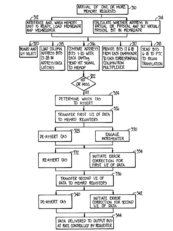
Referring now to Figs. 2 and 3, when the memory
system depicted in Fig. 2 is in the described normal
operative state, a memory read operation begins with a
memory read request arriving 310 over one of the address
buses 305, 307, 309. When more than one memory request is
present, arbitration logic in the receive state machine 112
arbitrates among these requests 312 and, according to a
predetermined priority system (and after the memory system
is in a condition to receive the next memory request), sets
the multiplexer 91 to convey one of the requested memory
addresses to the MemRqAdr register 90. Also during this
time, data which is on the data buses 84A, 84B, 84C, 84D,
is routed through multiplexers 86a, 86b to data registers
MemRqDataOd 68 and MemRqDataEv 66. Because the request
being considered presently is a read request, the data on
these data buses is spurious, i.e., it represents whatever
data, if any, happens to be on the data buses at that time.
Thus, this data is unrelated to the read request, and will
be unused. Also during this time, a logic circuit 93 is
used to determine 314 whether the memory request, which has
been admitted through the multiplexer 91, is a physical
address or a virtual address. This determination can be
made based on which of the address buses the address request
originated from and, in some cases, portions of the memory
specification code which is associated with that memory
request. The logic 93, after calculating whether the
address is virtual or physical, sets a bit in the MemRqAdr
register 90 to indicate whether the address is virtual or
physical 314.
- 27 2020275
In the next stage of the operation, five
procedures are initiated at approximately the same time:
the loading of a column address 315, a comparison 316,
maintaining of bits 317, initiating translation 318, and
board and XY select 320.
The bits from the MemRqAdr register 90, which
constitute eight of the ten column address bits, reside in
bit positions 21-28. During loading of the column address
315, these bits are routed through an address bus 130 to an
incrementer bus 132 to arrive at incrementers 88a and 88b.
The three least significant word address bits (in a cache
fill) will always be zero. This is because a cache line is
eight words (23) and the first word in the line has an
address for which the last three bits are 000. In the first
half of the read operation, the address which arrives
through incrementer 88a is unincremented (i.e., incremented
by zero), and bits 21-28 (20, Fig. lOC) passed through a
column/row multiplexer 54 which, in the current state, is
set for "column," and passed through the address latch 53a
to an address register bus 134a. The column address which
passes through the second incrementer 88b is incremented by
one, and bits 21-28 (20, Fig. lOc) are passed through a
second column/row multiplexer 56, also set to "column,"
through the address latch 53b, to a second address register
bus 134b. The addresses arriving through the address latches
53a, 53b thus contain only some of the column address bits,
namely, bits 21-28. Furthermore, it is important to note
that the address latches 53a, 53b will change contents for
each memory access request.
20~027~
28
In order to complete the ten column address bits
required for a full column address, two additional column
address bits are supplied to each of the memory banks 32,
34, 36, 38, through column/row multiplexers 58, 60, 62, 64,
which are set to "column." However, unlike the column
address bits which pass through the address registers 53a,
53b, these two column address bits, corresponding to bits 17
and 18 of the physical address, are not supplied directly
from the MemRqAdr register. Rather, these bits are provided
from the four physical address registers, or CAMPhyAdr A, B,
C, and D, 74, 76, 78, 80. It is possible to supply two
column address bits from these registers, because these two
column address bits are unchanged or constant as long as
there has not been a CAM miss indication. As described more
fully below, these two column bits change only when there is
a CAM miss. In this way, the two column address bits 17 and
18 supplied by the CAMPhyAdr registers 74, 76, 78, 80 act in
a manner similar to row address bits. Accordingly, the
process depicted in Fig. 3 includes maintaining these two
bits 317 from each CAMPhyAdr register to each corresponding
row/column multiplexer 58, 60, 62, 64.
Although each of the four row/column multiplexers
58, 60, 62, 64 provides two bits (for a total of eight
bits), only one of these multiplexers (i.e., only two bits)
will be used during any one memory access. This is because
a column address strobe will be asserted over only one of
the four banks 32, 34, 36, 38 of memory.
During the same time, four comparisons 316 take
place. The comparisons which are made are comparisons
2~2û2~3
29
between the bits from the MEMRqAdr register 90 and the
contents of each of the CAMTag registers 94, 96, 98, 100.
The bits to be compared with the CAMTag registers include
the row address, board select bits, X/Y select bit, and bank
select bits, along with the virtual/physical bit which has
been set by the virtual/physical logic 93. The 20 bits
which reside in each of the CAMTag registers 94, 96, 98, 100
also contain virtual or physical row address bits (from a
previous memory access), board select bits, bank select
bits, an X/Y select bit, and a virtual/physical bit. The
comparisons are done by four comparators 102, 104, 106, 108
which receive inputs from the CAMTag registers 94, 96, 98,
100 and from a virtual/physical bus 136, which is in
communication with the address bus 130.
Each comparator 102, 104, 106, 108, which finds an
identity between its two inputs, generates a hit signal and
transfers this hit signal to the MEMOP state machine 114.
In the preferred embodiment, there is a direct mapping
between the CAMTag registers 94, 96, 98, 100 and the four
memory banks 32, 34, 36, 38. Under such direct mapping,
CAMTagA 94 will only contain an address corresponding to
memory addresses in the first bank 32, CAMTagB 96 will only
contain an address corresponding to the memory contents of
the second bank 34, and so on. Because of the direct
mapping aspect, in normal operation, at most one of the four
comparators 102, 104, 106, 108 will indicate a hit.
At this point, the MEMOP machine 114 contains an
indication of whether or not there has been a hit, and which
of the four banks A, B, C, D, (32, 34, 36, 38) contains the
20202~
hit. The selection of the X or Y portion of memory 320 is
controlled by bit 6, which is output by the CAMPhyAdr
registers 74, 76, 78, 80 for output to the column address
strobe logic 152, 154, 156, 158.
Also at this time, virtual-to-physical translation
is initiated 318. As noted above, the address which is in
MemRqAdr register 90 may be either physical or virtual. The
results of a virtual-to-physical translation will only be
used when (1) the content of MemRqAdr 90 is a virtual
address, and (2) there has been no hit with any of the four
CAMTag registers 94, 96, 98, 100. However, because the
virtual-to-physical translation takes a number of machine
cycles to accomplish, the translation is initiated at this
time so that, should the translation prove necessary (as
depicted in Fig. 5), the translation process will have begun
before the results are determined to be necessary. In those
cases when translation is not necessary, the results of the
translation will be ignored.
The subsequent portions of the operation depend on
whether there has been a CAM hit 322, which, as noted above,
is a determination which has, at this point, been made by
the MEMOP state machine 114. In the scenario depicted in
Fig. 3, one of the CAMTags 94, 96, 98, 100 indicates a hit
with respect to bits 1-20 from MemRqAdr 90. For ease of the
following discussion, it will be assumed that the hit is
indicated by the second comparator 104. As will be apparent
to those skilled in the art, the following discussion will
be applicable, to a hit indication by any other comparator
102, 106, 108.
~ Q 7~27~
31
Because there has been a hit in the second
comparator 104, the second row address latch 44 contains the
row which includes the memory element being requested. This
fact is indicated, since the corresponding (second) CAMTag
96 contains the row address for the row stored in the second
row address latch 44. The row address in the second CAMTag
96 may be either a physical row address or a virtual row
address. However, regardless of whether the row address in
the second CAMTag 96 is virtual or physical, when there is
identity between a CAMTag 96 and bits 1-20 of the MemRqAdr
90, the address which is being requested must reside in the
row addressed by the contents of the corresponding row
address latch 44. In this way, it is possible to obtain a
CAM hit without having to wait for a virtual-to-physical
translation. The efficacy of this scheme is promoted by the
above-noted locality of "virtualness," i.e., the fact that
once a virtual or physical address request is made,
subsequent requests for memory elements in the same row are
highly likely to be of the same type (i.e., virtual or
physical).
As noted above, portions of a column address have
passed through the first two column/row multiplexers 54, 56,
and other portions pass through the remaining column/row
multiplexers 58, 60, 62, 64. After these addresses have
settled, in order to select the requested column from the
row addressed by the second row address latch 44, a column
address strobe must be asserted to the second bank of memory
34. As noted above, the MEMOP state machine 114 contains an
indication that the second bank, B, 34 contains the memory
~2~,~7~
32
element corresponding to the hit indication. Therefore, the
MEMOP state machine asserts a column address strobe (CAS)
324 to the second bank of memory 34.
In the preferred embodiment depicted in Fig. 2,
transfer of read data during a read is achieved in two
stages: one-half of the requested data is transferred to
the output register 116, the addresses are appropriately
incremented, and the second half is transferred. Referring
again to Fig. 3, following the assertion of the column
address strobe 324, one-half of the data is transferred 326
to the MemRd register 116. Next, the MEMOP state machine
114 simultaneously deasserts 328 the column address strobe
and engages 330 the incrementers 88A, 88B. Engaging the
first incrementer 88A causes that incrementer to increment
the address which passes through that incrementer by 4.
This incrementation corresponds to setting a single bit of
the address from a 0 to a 1. Similarly, the second
incrementer 88B also increments the address passing through
that incrementer by 4. The incremented addresses are passed
through column/row multiplexers 54, 56, (both set to
"column") to the address latches 53a, 53b.
At this point, simultaneously, the MEMOP state
machine 114 initiates the error correction logic 120A, 120B
for correction of error in the first half of the read data
334, and reasserts CAS 322. Because of the reassertion of
CAS 332, following incrementation 330 (and following
enabling the proper latches in the data register 116),
transfer of the second half of read data 336 is accomplished
to the MemRd registers 116. Next, simultaneously, the CAS
Q~20~ ~ a
33
is deasserted 340, and error correction for the second half
of read data is initiated 342. Finally, read data from the
error correction circuitry is delivered 344 to data
registers 122A, 122B, and thence through gates 126A, 126B,
controlled by board output enable logic 150, to data output
buses 124A, 124B.
Referring now to Fig. 4, a second operation is
depicted which includes a memory write when there is a CAM
hit. The initial stages of this operation are similar to
those described above in connection with a read operation.
One or more memory requests arrive 410, and the requests are
arbitrated 412. The requested address is sent to MemRqAdr,
and the write data arrives over the data buses and is sent
to MemRqData registers 66, 68. In this case, the write data
is real data (as opposed to the spurious data of the read
request). Also at this time, it is determined whether the
address is virtual or physical 414, and the virtual/physical
bit in MemRqAdr is set. Next, simultaneously, the column
address bits are loaded 415, and maintained 417, a
comparison is done with the CAMTags 416, and virtual-to-
physical translation is initiated 418. At the same time as
these steps, the write data is sent from the data register
66, 68 to error correction code check bit generators 70, 72,
and thence to the latches in the write data register 52.
In the process depicted in Fig. 4, the MEMOP state
machine 114 determines that there has been a CAM hit 422
and, accordingly, determines on which of the four memory
banks 32, 34, 36, 38 to assert the CAS and write enable (WE)
424. The write enable is asserted first and, following a
f~234
delay of one cycle, the column address strobe is asserted.
Assertion of the column address strobe and write enable
causes transfer of the write data 446 from the write data
register 52 to one of the memory banks 32, 34, 36, 38.
Following the transfer, the column address strobe is
deasserted 448.
It will be noted that, with respect to the
operations depicted in Figs. 3 and 4, the reading and
writing of data is accomplished with assertion and
deassertion of the column address strobe. During both of
these operations, the row address strobe is continually
asserted. The operations depicted in Figs. 3 and 4, using
assertion and deassertion of only the column address strobe,
are relatively fast. According to the present invention,
full advantage is taken of this relatively fast operation,
because it is done without the necessity of obtaining a
virtual-to-physical translation of the address. Although
such translation is initiated in all cases, once it is
determined that there is a CAM hit and that, consequently,
the translation will not be needed, the operation proceeds
without waiting for such translation to be completed. This
relatively fast transfer of data enables relatively fast
cache fills and high write bandwidths.
Referring now to Fig. 5, a process, which can be
either a read process or a write process, but in which there
is a CAM miss with respect to all four CAMTags 94, 96, 98,
100, is depicted.
The first portion of the process is similar to the
first portion of the process of Figs. 3 and 4. One or more
2132~27~
memory requests arrive 510, and are arbitrated 512 with the
address being sent to MemRqAdr and the data from the data
buses being sent to MemRqData 66, 68. It is determined
whether the address is virtual or physical, and the
virtual/physical bit is set in MemRqAdr 514.
Simultaneously, column address bits are loaded 515, and
maintained 517, a comparison is done with each CAMTag 516,
and virtual-to-physical translation is initiated 518. In
this case, the MEMOP state machine 114 determines that there
has been no hit on any of the CAMTags 94, 96, 98, 100,
constituting a CAM miss 522.
Subsequent processes depend on whether the address
which resides in MemRqAdr 90 is a virtual address or a
physical address. This determination is made 550 by the
MEMOP state machine, using the virtual/physical bit, which
has been calculated by the virtual/physical logic 93. If it
is determined that the address in MemRqAdr 90 is a physical
address, the row address bits (bits 7-16), along with the
X/Y select bit, bit 6, are sent directly to the PhyAd bus
142 through gate 144.
If the address in MemRqAdr is determined to be
virtual, it is necessary that the virtual-to-physical
address translation be used. As noted above, the virtual-
to-physical address translation was previously initiated
518. This translation is done using a hash scheme,
employing hash logic 95, in a manner well known in the art.
The hashed address is used as a look-up index in the lower
half 92a of the PTC entry table 92. The lower half 92a and
upper half 92b of the entry tables are duplicates of each
2~7~2~
36
other. Normally, the lower half 92a is used. However, if
an error is detected 553 when trying to access the lower
half of the page table cache 92, the spare select switch 160
is activated in order to access the upper half or "spare"
PTC entry table 92b.
After translation is accomplished, the results of
the translation are sent 560 to the PhyAd bus 142. Once the
row address, either directly from the MemRqAdr register 90
or as a result of the translation 560, is available on the
PhyAd bus 142, the process can continue. In the present
embodiment, even when the MemRqAdr address is physical, a
delay 562 is initiated to take up the amount of time which
would be required if a translation of a virtual address were
done.
Next, bits 19 and 20 on the PhyAd bus 142 are
observed by the MEMOP state machine 114 in order to
determine which of the banks 32, 34, 36, 38 must be updated
564. Note that, in this embodiment, two bits are needed to
specify the bank, since there are four banks. In other
embodiments, more or fewer banks could be used in connection
with more or fewer bank determination bits. For ease of the
following discussion, it will be assumed that the memory
request is for a memory element residing in the second bank
34 of memory. As will be apparent to those skilled in the
art, the following discussion will be applicable, to a
memory request for an element residing in any other bank 32,
36, 38.
In the next step, three operations are conducted
simultaneously: a deassertion of RAS 566; a loading of the
2~0%75
37
CAMTag 568; and a loading of the CAMPhyAdr 570. The row
address strobe is deasserted 566 only with respect to the
second row address latch 44, corresponding to the bank 34,
which needs updating, as determined previously 564. The
second CAMTag 96, corresponding to the second bank 34 which
is being updated, is loaded 568 with bits 1-20 directly from
the MemRqAdr register 90. It may be either a virtual
address or a physical address. By loading either a virtual
or a physical address into the second CAMTag 96, subsequent
requests of the same type (i.e., virtual or physical) which
are made for memory elements in that row whose address is
being loaded into the second row address latch 44 will
generate a hit with respect to the second CAMTag 96.
At the same time, the physical address which
resides on PhyAd bus 142 (along with other bits which are
stored in the CAMPhyAdr register, such as board select bits,
bank select bits, and parity bits, as described above) is
loaded, over the PhyAd bus 142, into the second CAMPhyAdr
register 76, which corresponds to the second bank 34. In
this way, both the second CAMPhyAdr register 76 and the
second CAMTag 96 are updated to reflect the physical row
address and the virtual or physical row address,
respectively, of the row which is being loaded into the
second row address latch 44.
The row/column multiplexers 54, 56, 58, 60, 62,
and 64 are all switched to "row" 572. The row address
constituting bits 7-14 are sent over a first row address bus
166 from the second CAMPhyAdr register 76, through the first
two column/row multiplexers 54, 56 to the address latches of
2~ ~27~
38
the write data register 52. At the same time, bits 15 and
16 of the row address are sent 576 from the second CAMPhyAdr
register 76, over the row address bus 166 to the
corresponding (second) column/row multiplexer 60. At this
point, the row address strobe is reasserted 578. The
column/row multiplexers 54, 56, 58, 60, 62, 64 are switched
to "column" 580, and the memory access which caused the CAM
miss is retried 582.
As noted above, in the preferred embodiment, the
computing environment contains a plurality of functional
units or memory units 93a (each typically residing on one or
two boards), such as that depicted in Fig. 2. Accordingly,
a system is provided for determining whether the requested
memory resides on a particular memory unit 93a and for
assuring that memory which is not on a given memory unit 93a
is not read from or written to that memory unit 93a. To
achieve this goal, each CAMPhyAdr 74, 76, 78, 80 includes a
board-select bit. The value of each board-select bit 912 is
computed during the procedures following each CAM miss.
Each memory unit contains a device 138 for storing an
indication of the "board base" and an indication of the size
of a particular memory unit (~3~, 32 or 64 megabytes). The
board base and size are loaded in each memory unit 93a at
power-up. The board base indicates the starting address of
the memory unit. From the starting address of the memory
unit and the size of the memory unit, the range of addresses
residing on that memory unit can be determined. During the
procedures following a CAM miss, the requested address is
compared, using comparator 146, to the range of addresses on
~2~2~3
39
the memory unit, and the board select indicator 148 is
produced, indicating whether the requested address is on
that memory unit. The board-select indicator 148 is stored
in the corresponding CAMPhyAdr 74, 76, 78, 80 as the board
select bit 912. During a write operation, if the board-
select bit 912 for that CAMPhyAdr 74, 76, 78, 80, for which
there has been a hit, indicates that the address does not
reside on that memory unit, the column address strobe is not
asserted, and thus writing to that memory unit is prevented.
During a read operation, if the board-select bit 912 in the
CAMPhyAdr 74, 76, 78, 80, for which there has been a hit,
indicates that the requested memory does not reside on that
memory unit, the MEMOP state machine 114, using board output
enable logic 150, prevents the data from being transmitted
through the memory unit output buses 124.
Referring now to Fig. 6, there is illustrated a
procedure used during the refresh of a dynamic memory, such
as that depicted in Fig. 2. In the preferred embodiment,
refresh is done in a "burst" manner. In this scheme, a
block of memory is refreshed during a given refresh cycle.
The size of the block which is refreshed and the delay
between refresh cycles are selected in order to provide, on
average, the needed frequency of refresh for any individual
memory element. The refresh is preferably timed to be
coordinated with RAS assertion time specifications (i.e.,
that period of time which the FPDRAM manufacturer specifies
as being the maximum time period that the RAS can safely be
continuously asserted). Preferably, a refresh cycle or
burst is delayed, when possible, until about such time as
2 0 ? ~ ~7 3
the maximum time specified by the memory manufacturer for
RAS assertion has passed. In this way, memory refreshes can
be used not only to comply with the needed frequency of
dynamic memory refresh, but also to comply with maximum RAS
assertion specifications.
The refresh is done for the entire memory. The
memory refresh is followed by RAS restoration, done in a
bank-wise fashion, as described below. In the following,
the refresh will be described in a preferred scheme in which
the order of RAS restore is bank A, bank B, bank D, and bank
C (i.e., according to a Gray code). Other orders of refresh
are possible, as will be apparent to those skilled in the
art.
Referring to Fig. 6, during an initial portion of
the refresh operation, all CAS and RAS signals are
deasserted. Next, four rows of all DRAMs 30 are refreshed.
Preferably, several refresh cycles are used, e.g., four or
eight refresh cycles.
During the final portion of the refresh operation,
RAS restoration is done bankwise. Memory bank A is selected
610 for RAS deassertion, and, simultaneously, the row/column
multiplexers 54, 56, 58, 60, 62, 64 are switched to "row"
612. The row address residing in the first CAMPhyAdr
register 74 is routed over the row address bus 166 in a
Z5 manner similar to that described above in connection with a
CAM miss 574, 576. Next, RAS is reasserted 618 to the first
memory bank 32, causing the same row address which formerly
resided in the first row address latch 42 to be loaded back
- 2~275
41
into that row address latch 618, substantially as described
above in connection with a CAM miss 578.
It can thus be seen that, following the refresh of
the first bank of memory 32, the row address latch 42 will
be in substantially the same configuration as before the
refresh, and thus will maintain its correspondence to the
first CAMPhyAdr register 74 and the first CAMTag register
94. Following the assertion of RAS, the bank selection is
incremented to bank B 620, and RAS restoration is completed
622 with respect to this bank. The refresh, with respect to
banks B, D, and C, will also leave the row address latches
44, 48, 46, CAMPhyAdr registers 76, 80, 78, and CAMTag
registers 96, 100, 98 in substantially the same condition as
before the refresh. In this way, following the complete
refresh cycle, the access of memory can continue in the same
manner as before the refresh, taking full advantage of the
locality structure and information inherent in the contents
of the CAMPhyAdr registers 74, 76, 78, 80, CAMTag registers
94, 96, 98, 100, and row address latches 42, 44, 46, 48,
which had been built-up before the refresh cycle.
In some computer operations, mainly diagnostic and
error recovery operations, it is desired to read the
contents of the PTC entry table. When this is desired, a
data pathway is provided to transport data from the PTC
entry table to the data output buses 124. This data path is
from the PTC entry table 92 along the PhyAdr bus 142,
through a gate 170 to a portion of the RqData bus 82, and
thence to a PTC entry bus 172 for delivery through
multiplexers 174, 176, to output registers 116, and
2 ~ ~ ~ 2 7 ~
42
eventually to output data registers 122 and data buses 124.
Operation of the memory unit, as described above,
is controlled largely by three state machines: MEMOP state
machine 114, the receive state machine 112, and the refresh
state machine 115. Each state machine operates somewhat
independently of the others, although, where noted below,
states for some state machines will be coordinated with
particular states for other state machines, and certain
state transitions in one state machine are dependent on the
status of another state machine.
In the following, operation of the state machines
will be described with respect to state diagrams. In the
state diagrams, the solid-boxed elements represent states of
the state machine, and the solid lines with arrows indicate
transitions from the present state to the next state.
Dashed boxes with dashed arrows, ending on the solid arrows,
indicate conditions which must be satisfied for the
indicated transition to take place. An asterisk (*) with a
condition indicates a logical "not." RqOp indicates the
"requested operation." A "v" indicates a logical "or." An
ampersand (&) indicates a logical "and." A "<>" symbol
indicates "not equal to."
The MEMOP state machine 114 handles all non-
refresh accesses to the memory and all accesses of the PTC
entry table. Once a request has been accepted, the logic of
the MEMOP state machine 114 decodes the request and sends
control signals to CAS and RAS control PAL's (programmable
array logic) (not shown) to indicate when to strobe signals
for the memory array 30. In addition, the MEMOP state
~ Q ~
machine 114 indicates to the receive interface (not shown)
when read data from the memory 30 is ready to load into the
staging registers 122, and indicates to the CAMPhyAdr 74,
76, 78, 80 when data from the PTC entry table 92 is ready to
5 load for CAMPhyAdr updates. The MEMOP state machine 114
arbitrates between requests for memory refresh and requests
for memory accesses from external requesters. The MEMOP
state machine 114 stops operation only in a start or idle
state 710 (Fig. 7).
Referring to Fig. 7, the MEMOP state machine 114
will cycle 711 to remain in the start state 710 as long as
either (1) the MEMOP state machine is not yet ready to
initiate a new operation (indicated by MemOpRdy*=true), such
as when the MEMOP state machine is already engaged with a
15 conflicting operation or when initiation of an operation in
the MEMOP state machine would conflict with operation of
another state machine, or (2) when the requested operation
is for a diagnostic write (RqOp=DiagWrite). The MEMOP state
machine will remain in the start state 710 during refresh
20 cycles (described below).
From the idle or start state 710, the MEMOP state
machine 114 can undergo a transition to one of four states.
In a memory read request with CAM hit, the initial
transition is to the MEMRdl state 712. In a memory write
25 request with CAM hit, the initial transition is to the
MEMWrl state 714. In a PTC write request, the initial
transition is to the PTCWrl state 716. A fourth state,
PTCRdl 718, is used in connection with a CAM miss, a PTC
read request, or a diagnostic read request. Transition to
~ 0 2 `~
44
any of these four initial states requires that the MEMOP
state machine 114 be ready (i.e., MemOpRdy = true).
The operation of the MEMOP state machine 114
during a read request with CAM hit corresponds generally to
the memory operation discussed above in connection with Fig.
3. As depicted in Fig. 7, when the request being honored is
a read request (i.e., RqOp=MemRead), and there has been a
CAM hit indication (i.e., AnyCAMHit=true) 720 from one of
the four comparators 102, 104, 106, 108, the MEMOP 114
enters the state MEMRdl 712. During MEMRdl, look-up of data
in the DRAM is initiated. After engagement of the
incrementer 88a, 88b, CAS is asserted. MEMOP 114 then
undergoes transition to the state MEMRd2 722. During this
state, the first cycle of memory read access is completed,
i.e., the first group of four words is transferred to the
MEMRd registers il6. Transition from MEMRd2 depends upon
several factors. If the receive machine is non-idle,
indicated by the signal RcvIdle* being "true" 724, the MEMOP
machine will remain in MemRd2 722 for one cycle. The signal
MemRd2R* indicates that MEMOP 114 is in state MemRd2 for the
first cycle. On the next cycle (MemRd2R=true), if RcvIdle*
is still true 726, then MEMOP 114 will return to the start
state 710 and attempt to read again.
If the receive machine 112 is idle (RcvIdle=true),
the transition from MemRd2 depends upon which type of read
request was made. A first type of read request, termed
"Read 2," results in the transfer of two words. The second
type of read request, termed "Read 8," transfers up to eight
words back to the requester. Read 8 is typically used in
- 45 2`~202~
connection with a cache fill operation. If the request was
for a Read 2 operation, this will be indicated by RqOp <3> =
true 728. In this case, MemRd2 722 will undergo a
transition to the start state 710. If the request was for a
Read 8 (RqOp <3>* = true), the transition is to the
"Precharge" state 734. This state is an intermediate state
in which CAS is deasserted, while the addresses for the
memory 30 settle to a new value. Precharge 734 undergoes a
transition to MemRd3 736. During MemRd3 736, CAS is
asserted for access of the second half of the read data.
MemRd3 736 undergoes transition to MemRd4 738 to complete
transfer of the second group of four words (i.e., the second
half of the read data). MemRd4 738 undergoes transition to
the start state 710.
The second operation of the MEMOP machine 114
involves writing data to memory. This operation of the
state machine, corresponds generally to the procedure
discussed above in connection with Fig. 4. From the start
state 710, MEMOP 114 will undergo transition to MemWrl 714
when there has been a memory write request (RqOp=Mem Write)
with a CAM hit 742. During MemWrl 714, the write enable
signal is asserted to all DRAM's. The CAS signal is
unasserted while addresses to the DRAM's settle. From the
MemWrl state 714, MEMOP 114 undergoes a transition to MemWr2
744. During this state, memory write operations are
completed. The write enable remains asserted to all DRAM's
and CAS is asserted. Transition from the MemWr2 state 744
depends upon whether there is, pending, a second write
request. When there is no CAM hit or if MEMOP is not ready,
- 2 0 ~ ~ 2 7 J
46
or if there was no pending write request (RqOp c> MemWrite)
746, MemWr2 744 undergoes transition to the start state 710.
If there is a CAM hit, MEMOP 114 is ready, and there is a
pending write request (RqOP = MemWrite) 748, MemWr2
undergoes a transition to MemWrl 714.
The third operation of the MEMOP 114 is a request
to write to the PTC entry 92, such as when the PTC entry 92
is to be updated. As seen in Fig. 7, the MEMOP 114 will
undergo a transition to PTCWrl 716 if there has been a PTC
write request (RqOp=PTCWrite) 752. Thereafter, MEMOP 114
will invariably undergo transitions successively to states
PTCWr2 754, PTCWr3 756, PTCWr4 758, and PTCWr5 762,
whereupon MEMOP 114 will return to the start state 710. In
PTCWrl, the CAM's are invalidated at the end of the cycle.
The PTC write enable becomes active during this cycle.
During PTCWr2 754, PTC write enable becomes inactive.
During PTCWr3 756, the PTC address is changed from bank 0 to
bank 1 so that the second bank 92b will be written with
write data during PTCWr4 758 and PTCWr5 762. During PTCWr4
758, PTC write enable becomes active, and during PTCWr5 762,
PTC write enable becomes inactive.
The final operation of MEMOP 114 occurs during a
CAM miss (AnyCAMHit* and RqOp <0>), generally as depicted in
Fig. 5, or during a PTC read request (RqOp=PTCRd) or a
diagnostic read request (RqOp=DiagRd). Under any of these
conditions 764, as depicted in Fig. 7, there is a transition
of the MEMOP state machine 114 to PTCRdl 718. The MEMOP 114
undergoes successive transitions to PTCRd2 768 and PTCRd3
772. In the described embodiment, PTC access is relatively
- 20~!)27~
47
slow, largely because the PTC entry device 92 is a slow
access device. Accordingly, three cycles 718, 768, 772 are
needed to complete the access. However, since a CAM miss
will not occur on every memory access, such occasional slow
access does not seriously degrade overall performance. If
the request was either a PTC read request or a diagnostic
read request 766, MEMOP 114 undergoes transition from PTC
Rd3 to the start state 710. In the case of a CAM miss 774,
PTCRd3 772 undergoes transition to PTCRd4 776. During
PCRd4, PTC parity errors are checked. If there is no parity
error 778, PTCRd4 776 will undergo transition to the start
state 710. If there is a PTC parity error in PTC bank 0,
782 of either functional unit (MUOPTCParErr or
MUlPTCParErr), the operation is a Read 2, Read 8, Write 1,
or Write 2 operation (RqOp=OOxx), and the PTC array is not
being bypassed (PTCArrayBypass, used principally during
board testing), access to bank 1 of the PTC will be
attempted. An access of bank 1 occurs during three cycles,
PTCRd5 784, PTCRd6 786, and PTCRd7 788.
The receive state machine 112 handles the transfer
of read data from the memory board to the selected
requester. It controls the loading of the RDData registers
122 along the read-data path. It also selects words for ECC
correction 120 during memory reads. The receive state
machine 112 has two types of operation: Read 2-type and
Read 8-type. The Read 2 operations transfer two words,
while the Read 8 operations transfer up to eight words back
to the requester. The receive state machine 112 will remain
in the idle state 792 if the MemRd register 116 is not
~2~275
-
48
loaded (LdMemRdLo*) or the operation is a Read 8 operation
(RqOp=Read8), provided the data in the MemRd register 116 is
not yet indicated as valid (MemRDVld*).
During the Read 2 operation (indicated by RqOp<>
Read8), the receive machine 112 will undergo a transition
from the idle state 792 to ECCRd2 794 when valid data has
been loaded into O:l of the MemRd register 116 by the MEMOP
114 state machine (indicated by MemRdVld = true or LDMemRdLo
= true) 796. In the ECCRd2 794 state, the receive state
machine 112 is performing ECC correction. ECCRd2 794
undergoes transition to TRd2 798. In the TRd2 state 798,
data obtained in accordance with a MemRd2, PTC Read, or
Diagnostic Read, as discussed above, is transferred to the
requester. The receive state machine 112 remains in this
state 798 as long as Rcv and LRcv are unasserted (Rcv* and
LRcv* = true) 802. Rcv indicates that a receiver is
initiating receipt of data. LRcv indicates that a receiver
is initiating receipt of the last portion of data which was
requested. When either LRcv or Rcv is true 804, the machine
undergoes a transition to the idle state 792.
For a Read 8 operation, the receive state machine
112 will undergo a transition from the idle state 792 to
ECCRd8 808 when a Read 8 request is pending (RqOp = Read8)
and there is valid data in 0:1 of the MEMRd register 116
(i.e., MemRDVld = true) 806. In ECCRd8 808, the receive
machine 112 performs ECC correction and checking on data in
0:1 of MEMRd 116. Transfer of the read data to the
requester occurs by way of four transfers of double-word
data. These four transfers occur, respectively, during
202Z327S
~.
49
states T1 810, T2 812, T3 814, and T4 816. In each of these
four states, Tl T2, T3, and T4, the state machine will stay
in the respective state as long as neither Rcv nor LRcv is
asserted 818, 822, 824, 842. Asserting LRcv during Tl, T2,
T3, or T4 826, 828, 832, 844 will cause an immediate
transition to the idle state 792. When Rcv is asserted
during the Tl, T2, or T3 states 834, 836, 838, the receive
machine 112 will undergo transition to the next successive
state. Once the machine 112 reaches state T4 816, it will
wait in this state 842 until the requester asserts Rcv or
LRCv 844. The receive state machine 112 then undergoes a
transition to the idle state 792.
The refresh state machine 115, whose states are
depicted in Fig. 9, accomplishes two tasks. First, the
refresh state machine 115 controls the RAS and CAS controls
of the DRAM array. In this mode, the refresh state machine
is under the control of the MEMOP state machine 114. The
second task of the refresh state machine is to handle CAS-
before-RAS refreshes of the DRAM. In this mode, the refresh
state machine controls the RAS and CAS signals. A 12-bit
count-down counter (not shown) with a scannable reset value
of between 256 and 4096 (in multiples of 256 cycles)
triggers a single refresh request each time it rolls over.
Each such request causes the refresh machine to recycle
selectably through either four or eight CAS before RAS
refreshes prior to returning to an idle state 852. When the
refresh machine 115 is not idle, memory requests cannot be
processed. Thus, there are handshake signals between the
2~2~ ~
-
MEMOP machine 114 and the refresh machine 115 to ensure that
one of the two machines is always idle.
A signal which initiates the refresh cycle, termed
"Refresh Go," 854 is issued when the refresh counter
indicates that a refresh cycle is required and after proper
handshake protocol from the MEMOP state machine 114. Until
this signal is issued 853, the refresh state machine 115
remains in the idle state 852. The Refresh Go signal 854
causes a transition to a pause state 856. During pause 856,
all RAS and CAS lines are deasserted. Next, the refresh
state machine loops through states Rfshl 858, Rfsh2 862,
Rfsh3 864, Rfsh4 866, and Rfsh5 868.
The number of loops through states Rfshl-Rfsh5 is
kept track of RfshRowCtr. Preferably, the machine cycles
through four refreshes, as depicted in Fig. 9, or eight
refreshes. The description below relates to the four-cycle
option. As will be apparent to those skilled in the art,
the eight-cycle scheme will be similar, but with the
conditions on Rfsh5 872, 874 set to 7, rather than 3. In
each loop, RAS and CAS are deasserted during Rfshl 858, CAS
is asserted and RAS is deasserted during Rfsh2 862, and RAS
and CAS are both asserted during Rfsh3 864, Rfsh4 866, and
Rfsh5 868.
Following the last loop 874, Rfsh5 868 undergoes
transition to a wait state 876. If the Run Mode signal is
deasserted (RunMode* = true), the refresh state machine will
either remain in the wait state 876, if Refresh Go is
unasserted 878, or will return to the Rfshl state 858 if
Refresh Go is asserted 882. RunMode is used to ensure that
20~iO27~
51
an operation, once begun, is finished. The wait state 876
allows the address latches time to resolve themselves for
the first block's row address, so that when RAS is
reasserted (during RASRestore 892), the latches in the DRAM
devices will contain that information which the CamPhyAdr
and CAMTag registers indicate they have. When Run Mode is
asserted 884, following the wait state 876, there is a
transition to the latch state 886. The latch state 886
provides set-up time for the address latches to drive the
address lines so that the CAMTag registers 92, 94, 96, 98
and CAMPhyAdr registers 72, 74, 76, 78 can be revalidated.
Following the latch state 86, there is a
transition to the RAS restore state 892. During RAS
restores 892, RAS is asserted to one of the four blocks of
memory 32, 34, 36, 38, resulting in a reload of one of the
four row address latches 42, 44, 46, 48. The latch-RAS
restore cycle is repeated four times, counted by RfshRowCtr
894, once for each row address latch.
A number of variations and modifications of the
described invention can also be used. As will be apparent
to those skilled in the art, certain ideas disclosed herein
can be used independently of other ideas disclosed herein,
or in various combinations therewith. A memory can be
provided in forms other than fast page mode, such as static
column mode DRAM, and can be provided with more or fewer
than four blocks of memory. In general, larger numbers of
memory blocks (each having a corresponding CAMTag and
CAMPhyAdr) are effective to avoid or reduce thrashing, but
require more complicated and expensive hardware and
202~27~
52
software. The mapping between the CAMTags and the memory
can be a direct mapping, a set associative mapping, or a
fully associative mapping. The invention can be used in the
context of other memory hierarchies, and is not limited to
situations in which reads are conducted to perform a cache
fill. The present invention can also be used in a system
which has no memory hierarchy, but, rather, has access of a
single level of memory. The invention can be used with
memory sizes and address widths other than those described.
The invention can be used with an interleave system other
than the referenced four-way pseudo interleave, or with no
interleave system at all. In some embodiments of the
invention, it is possible to avoid updating a row address
latch following a CAMTag miss if the CAMTag miss was caused
only by non-identity of the column bits stored in the CAMTag
with corresponding portions of the address request, as shown
in Fig. lF.
With reference to Fig. 5, it is possible to
eliminate the delay 562 in order to take advantage of the
savings in time, which occurs when no virtual-to-physical
translation is needed. It is possible to initiate a
read/write operation immediately after the reassertion of
RAS 578 and switching of the multiplexer 580, rather than
retrying the memory access 582, for example, by initiating
the step of determining which bank the CAS is to be asserted
on, as depicted in Fig. 3 at 324, or in Fig. 4 at 424.
Although all six row/column multiplexers are switched to
"row" 572, it is possible to switch only those row/column
20-2~2 ~ ~
53
multiplexers which are needed in order to load the new row
address into a selected row address latch.
Although the refresh cycle preserves locality
information, as described above, it is possible to
reinitialize the memory system following a refresh.
In the present invention, there is some increase
in power consumption, because of the high percentage of time
during which the RAS is asserted. It is thus possible to
deassert RAS for a larger percentage of the time to reduce
power consumption, although at the cost of a decrease in
efficiency.
Although the present invention has been described
with reference to a preferred embodiment and certain
modifications and variations thereof, other modifications
and variations can also be practiced, as will be apparent to
those skilled in the art, the invention being described by
the following claims.