Note: Descriptions are shown in the official language in which they were submitted.
202û~43
p 39 22 486.4
Time-Division Multiplex Communicat;on System
with a Synchronizing Circuit at the Receiving
End which Responds to the Coding of Words In-
serted in the Transmitted Information
The present invention relates to a system as set forth in
thepreamble of claim 1. Such a system is disclosed in
DE-A1 37 35 377.
In this system, a so-called code word is derived from in-
formation referred to there as "header", which contains a
logic channel number, and transmitted subsequent to the
information. In common technical terms, the information
(K) is coded in a linear block code to form a code word
whose number of bits is equal to the number of bits of
theinformation (K) augmented by the number of added bits
(called "c~e word CW" there). The number of bits in the
code word consisting of the k-bit information (K) and the
added b;ts will hereinafter be denoted by n. In the prior
art system, such code words are inserted at the transmitting
end into the bit sequence at regular time intervals, namely
at the beginning of each so-called packet. At the receiving
end, the prior art system includes a checking device which
looks for the n-bit code words in the receivedbit sequence.
It does so by selecting a sequence of k bits from the
B. X. Weis 1
20203~
received bit sequence and checking whether this k-bit sequence
and the subsequently received n-k bits. (n-k is the number of
bits added to the information K at the transmitting end)
together represents a code word which is coded in the block
code. If the checking device determines that the checked bit
sequence is not coded in the block code, it will stop the
search for the code word in the current packet and resume it
in the next packet, in which it then selects a bit sequence
which, referred to the beginning of the packet, begins one bit
later than the bit sequence selected in the previously checked
packet.
This means that considerable time may elapse until
the n-bit word looked for is found in any packet. This, in
turn, has the disadvantage that the synchronization of the
receiver with the transmitter takes a long time, thus causing
considerable information losses.
It is therefore the object of the invention to
provide a time-division multiplex communication system of the
above kind in which the synchronizing device at the receiving
end finds the n-bit word faster, thus ensuring faster
synchronization.
According to one aspect, the invention provides a
time-division multiplex communication system comprising: a
transmitting device which regularly encodes an n-bit word in a
linear block code into a bit sequence to be transmitted and a
checking device at a receiving end which looks for the n-bit
word in the receiving bit sequence by checking groups of n
successive bits as to whether they are coded in the block
- 2 -
72430-117
2020343
code, wherein the checking device (SRl, SR2, Nl, to Nn k~ LS)
checks all n-bit groups (Xj to Xj+n 1) which begin with any
one of (Xj) of the n successive bits of the received bit
sequence by successively checking in parallel n-bit groups and
by independently checking each n-bit group.
According to another aspect, the invention provides
a method in a time-division multiplex communication system
having a transmitting device which regularly encodes an n-bit
word in a linear block code into a bit sequence to be
transmitted, and a checking device at a receiving end, for
checking for an n-bit word coded in a linear block code in a
received bit sequence by checking groups of n successive bits,
comprising the steps of: checking all n-bit groups (Xj to
Xj+n 1) which begin with any one (Xj) of the successive bits
in the bit sequence, by successively checking in parallel n-
bit groups and by independently checking each n-bit group.
According to yet another aspect, the present
invention provides a method for checking for an n-bit word
coded in a linear block code in a bit sequence by checking
groups of n successive bits, comprising the steps of: storing
a selected number of the bit sequence; calculating each
component of the syndrome (Sl to Sn k) from an n-bit group to
be checked; determining a magnitude from the calculated
components of the syndrome; successively and independently
checking all n-bit groups (Xj to Xj+n 1) which begin with any
one (Xj) of the successive bits in the bit sequence; and
delaying the received bit sequence until the check of an n-bit
group (Xj to Xj+n 1) is completed.
- 2a -
72430-117
~02~343
According to a further aspect, the present invention
provides a checking device for time-division multiplex
communication system having a transmitting device which
regularly inserts an n-bit word coded in a linear block code
into a bit sequence to be transmitted comprising: storage
means, responsive to the transmitted bit sequence, for storing
the bits thereof for providing the stored bits; and
checking means, responsive to selected stored bits, for
checking groups of n successive bits as to whether they are
coded in the block code by checking all n-bit groups
(Xj to Xj+n 1) which begin with any one (Xj) of the successive
bits, by successively checking in parallel n-bit groups and by
independently checking each n-bit group.
Aside from making it possible to quickly find the
n-bit words coded in the block code, the invention has the
advantage that none of the parts of the check circuit
- 2b -
72430-117
~ 2020343
requires a processing clock frequency which is higher than the
bit rate of the received bit sequence. Therefore, the
checking device can be implemented in CMOS technology and,
thus, at low cost even at a high bit rate of 150 Mb/s. Any
circuit operating at higher clock frequencies could only be
implemented in a more expensive technology , e.g., ECL.
Before the invention is described with reference to
the accompanying drawings, it will be briefly explained what
kind of mathematical check is used to determine whether the
bit group is coded in the linear block code. Such a block
code is commonly referred to as an (n,k)- block code, where n
is the total number of bits per block, and k is the number of
information bits per block.
According to a particular embodiment of the
invention the checking of an n-bit group as to whether it is
coded in the linear block code is done by calculating the
syndrome on the basis of the parity check matrix of the linear
block code used. That is not the case with the above-
mentioned prior art checking device. As is well known, the
syndrome, hereinafter denoted S, is a vector of dimension n-k
and is calculated by multiplying the transpose of the parity
check matrix H of the block code by the received block,
hereinafter denoted X. Further details are described in a
book by W.W. Peterson, "Error-Correcting Codes", Massachusetts
Institute Of Technology and John Wiley & Sons, Inc., New York,
London, 1961, pp. 30-36.
- 3 -
72430-117
2~2~43
-- 4
The ith component of the syndrome must be calculated
from an n-bit block and the transpose of the parity
check matrix as the scalar product of the ith row hi
and the received block X, i.e.,
Sj=hjX=hj1X1+hj2X2+hi3X3 in n
These components of the vector S are calculated by the
check circuit according to the invention for each n-
bit bit group which begins with any one of the successively
received bits, i.e., for the first bit of the b;t sequence
and the next n-1 bits, one bit period later for the second
bit of the received bit sequence and the next n-1 bits, etc.
The syndrome calculation is commonly used for error de-
tection. A given data word is examined as to whether it
contains a code error, as in DE-A1 37 07 143, for example.
There, the syndrome calculation is not used to find out
at what point a bit sequence transmitted at a high bit
rate contains a word coded in the block code. The
implementation of the circuit disclosed in that publi-
cation also would be unsuitable for the present appli-
cation, since it uses memories in which partial syn-
dromes are stored, and since such a circuit, because of
the memory access times and the EXCLUSIVE-OR gates
folLowing the memories, would require too long a pro-
cessing time for the present application.
In the following, it will be explained with the aid
of the accompanying drawings how the calculation and
B. X. Weis 1
2 0 2 ~ 3 1 3
checking of the syndrome S are performed for each n-bit
bit group beginning with a bit of the received bit se-
quence.
The invention will now be explained in greater detail,
by way of example, with reference to the accompany;ng
drawings, in which:
Fig. 1 is a block diagram of the checking deYice
at the receiving end of the system accord-
ing to the invention;
Fig. Z shows an embodiment of one of the networks
N1 to Nn-k of Fig- 1;
Fig. 3 shows the logic diagram of one of the ele-
ments E1 of Fig. 2, and
Fig. 4 shows the logic diagram of one of the elements
E2 of Fig. 2.
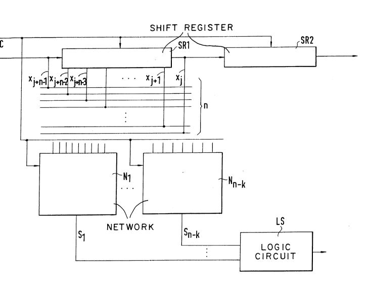
In the checking device shown in Fig. 1, the received bit
sequence is applied to the serial input of a shift re-
gister R1 having a length of n-1, i.e., n-1 series-con-
nected flip-flops, if the code word to be found contains
n-bits. Such a shift register has n-2 parallel outputs,
so that n successively received bits of the bit sequence
are made available in parallel for further processing.
If the bit appearing at the output of the shift register
SR1 at any defined point of time is denoted Xj, the sub-
sequent bits of the n-bit bit group beginning with the
B. X. Weis 1
- 6 - 2~03 q3
bit Xj will appear simultaneously at the paralLel outputs
of the shift register SR1, where they are denoted xj+1 to
Xj+n-2' and at the input of the shift register SR1,
with the bit appearing at the input of the shift register
denoted xj+n 1. Since the shift reg;ster is controlled by
a clock signal C whose frequency is equal to the re-
ceived bit frequency, the n-bit word beginning with the
bit xj+1 is made available for further processing in the
next bit period.
The n-bit bit group made available for further processing
in any bit period of the received bit sequence is applied
in parallel to a bus designated n, of which selected
conductors are connected to the inputs of networks N1
to Nn_k which are arranged and operated in parallel.
For each syndrome component Sj to be calculated as de-
scribed above, there is one network, i.e., n-k networks,
because the syndrome has n-k components, as mentioned
above.
Of the n bits of the n-bit bit group to be checked, only
those bits are entered into a network N; for which the
associated value hjl is nonzero (above equation for Sj).
In the above equation for Sj, this means, for example,
that in the network N;, which calculates the component
S; of the syndrome if the values hj2 and hj3 are zero,
only the first, fourth, and subsequent bits of the n-
bit bit group are entered, while the bits appearing in
the second and third positions of an n-bit bit group,
no matter what binary vaLue they represent, are omitted.
Thus, based on the parity check matrix, a particular
B. X. Weis 1
2~1ft" Q3f~3
-- 7 --
selection of the n bits of an n-bit bit group to be checked
is entered into each of the n-k networks N1 to N k for
each component of the syndrome. The networks calculate
their component of the syndrome by the above equati~on
for S; in several stages.and, as will be explained w th
the aid of Fig. 2, deliver their components Si of the
syndrome simultaneously at their outputs, which are de-
signated S1 to Sn_k.
Since the h;l of the parity check matrix can only have
the value O or 1, and the additions given in the above
equation are modulo-2 additions, the calculation to be
performed consists of EXCLUSIVE-ORing the
input bits severaltimes, which, as is well known, yields
a 1 as a syndrome component in the presence of an odd
number of ones and a O in the presence of an even number
of ones.
The EXCLUSIVE-ORing of the input bits of one of the net-
works, which is performed in several stages, takes place
at the bit rate C of the received bit sequence. After a
given number of bit periods, the syndrome for the n-bit
bit group being checked is present at the outputs of
the networks. Its bits pass through a logic circuit LS,
which produces an output signal if the syndrome is zero
(all components), thus indicating the detection of
an n-bit code word.
B. X. Weis 1
. - 8 -
2~2~3
From the output of the shift register SR1, the bit se-
quence is applied to the serial input of a shift register
SR2, which, too, is operated at the bit rate of the bit
sequence and delays the bit sequence until the networks
Nj have calculated the syndrome for an n-bit bit group
beginning with the bit Xj. Thus, the first bit of a
bit group will appear at the output of SR2 when the logic
circuit LS indicates at its output whether this bit
group is a code word or not. The logic circuit LS introduces
no appreciable delay. If its delay should be too long,
it may be compensated by lengthening the shift register SR2
corresDondingly.
The advantage of the checking device described so far
lies in the fact that it checks the received bit se-
quence bit by bit without any delay and does not re-
quire a processing clock frequency which is higher than
the bit frequency.
An embodiment of one of the networks N; of Fig. 1 will
now be explained with the aid of Fig. 2. Fig. 2 shows
a network N; for calculating a component Sj(j) from a
bit group beginning with a bit Xj. The example assumes
that nine of the n bits of the n-bit bit group to be
checked, which begins with the bit Xj, have to be used
for calculating the component Sj(j) of the syndrome.
(For the other bits, the associated h;l are nonzero).
The bits to be used for the calculation are denoted at
the parallel inputs of N; by X(j-io) to X(j-i8).
In a stage ST1 of Nj, the input bits to be summed by
modulo-2 additions are combined into arbitrary pairs,
with each bit permitted to occur in only one pair. In the
B. X. Weis 1
2~2~3~3
-
_ 9 _
example shown, therefore, there are four pairs and one
remaining bit, because the number of bits is odd. Each
pair of bits is added modulo 2 in one of network ele-
ments of a first type E1 in a first clock period and
stored until the next clock period. The remaining bit
is stored in a network element of a second type E2
until the next clock period.
The functi~s of the elements of the type E1 and type
E2 are shown in Figs. 3 and 4~ respectively. An ele-
ment E1 contains an EXCLUSIVE-OR gate A1, which forms
the EXCLUSIVE-OR of two input bits applied at the in-
puts x and y, i.e., adds them modulo 2, and a succeeding
D flip-flop D1, which stores the result until receipt
of the next clock pulse. The D flip-flop is controlled
by the bit-rate clock C indicated in Figs. 1 and 2.
An element E2 serves to store a single bit applied at
its input X in a D flip-flop D2 until receipt of the
next clock pulse. It is also controlled by the clock C.
After the input bits of N; have been combined in pairs
and the results and the remaining input bits have been
temporarily stored in the first stage ST1 of N; in a
first clock period, the temporarily stored results and
the temporarily stored remaining bit of the stage ST
are processed in a corresponding manner in a stage
ST2 upon receipt of the next clock putse. The input bits
are again combined in pairs by elements E1, and the re-
maining bit is stored in an element E2. Upon receipt of
the next clock pulse, the results of stage ST2 are pro-
cessed in a corresponding manner in a stage ST3, and
upon receipt of a further clock pulse, a last stage ST4
~B. X. Weis 1
2023~ ~3
- 10 -
calculates, in an element E1, the result bit, i.e., the
component Sj(j) of the syndrome, from the results of
stage ST3. In the example shown, i.e., with nine inputs,
four stages are needed, so that four bit periods
after the first bit Xj of an n-bit bit group beginning
with this bit appeared at the output of the shift
registers SR1 of Fig. 1, the network Ni has calculated
the component Sj(j) of the syndrome of this bit group.
Each of the networks N; to N k has an individual number
of input bits to be combined and a corresponding number
Mj of stages necessary for this purpose. In order for
the entire syndrome S(j) of an n-bit bit group be-
ginning with the bit group Xj to appear at the outputs
of the network N; simultaneously, those networks whose
necessary number of stages M; is less than the greatest
M; occurring in any one of the networks have additional
stages including elements of type E2, so that all net-
works will make available their components Sj(j) of the
syndrome S(j) at their outputs at the same instant.
This instant is M bit periods ~ater than the in-
stant at which Xj appears at the output of the shift
register SR1 of Fig. 1, where M is the maximum number
of stages required in any of the networks N;. The delay
of the shift register SR2, mentioned above in connection
with Fig. 1, is thus M bit periods~ Thus, the
shift register SR2 delays the bit sequence until it has
~. X. Weis 1
2~2~3~3
been decided whether a particular bit group is a code word
or not.
It should be added that instead of a shift register SR1,
any other memory circuit can be used to make available
the n-bit bit groups to be checked. This may also be a
memory in which the bits of a received bit sequence are
stored other than serially provided that it is possible
to output successively received bits simultaneously as
one n-bit bit group.
To optimize the circuit, the networks Ni may be inter-
connected to permit the transfer of intermediate re-
sults from one network to another, thus reducing the
amount of circuit elements required.
B. X. Weis 1