Note: Descriptions are shown in the official language in which they were submitted.
,. ~O~a3'~9
PATENT
DIGITAL SYNTHETIC ySERRODYNE
FOR FIBER OPTIC GYROSCOPE
$ACKGROUND AND SUMMARY OF THE INVENTION
This invention relates to optical gyroscopes
in general and to a fiber optic gyxo wherein a
digitally synthesized serrodyne waveform is applied to
a single phase-modulator in a closed-loop fiber optic
gyroscope.
In fiber optic gyroscopes there exists an
analogy to traditional electromechanical rate gyros in
that either type may be operated "open-loop" or
"closed-loop". The closed-loop configuration
generally is associated with higher levels of
precision than the open-loop type. In an open-loop
lg gyro the basic device output is the direct measure of
gyro input rate. In a closed-loop gyro the output is
constantly maintained at null by means of an external
feedback mechanism which acts to cancel the inertially
sensed rotation. In the case of electromechanical
gyros this feedback consists of applying a precision
torque to the gyro's spinning rotor to maintain the,
alignment with the gyro case, the current needed to
apply the correct torque thus becoming a measure of
gyro input rotation. In the case of fiber optic
202~3'~9
gyros, the appropriate photodetector output current
component is continuously maintained at null by the
action of a differential phase shift transducer which
exactly cancels the phase shift induced by the applied
input rate (the "Sagnac" shift) to the two
counterpropagation light beams within the fiber. The
frequency of the signal voltage to the tranducer
becomes the measure of gyro input rate.
In order to generate the differential phase
shift, two basic approaches have been employed in the
past. One involves the use of acousto-aptic frequency
shifters (eng. Bragg cells) which directly change the
optical carrier frequency of an input light beam by
the amount of the applied signal voltage frequency.
Another approach to phase-shifting a light beam is to
employ a phase shifter which can vary or modulate the
optical path length within itsslf by application of a
signal voltage to it. These phase-shifters (which are
several) may be fabricated so as to be an integral
part of the fiber coil or formed with vibrating
mirrors, or made in integrated optic form or formed by
deposition of optically active material on optical
fiber. To generate a differential beam phase shift
equal and opposite to the Sagnac-induced (i.e. rate
induced) phase shift, a special electrical periodic
signal in the shape of a sawtooth (a serrodyne
waveform) is applied to the phase shifter. The
-2-
t
repetition rate of this periodic waveform then becomes
the gyro output, along with an additional output to
specify the direction of input rate (polarity).
A problem that arises with such a serrodyne
modulator when gyro input rates are low is that it
becomes difficult to generate the serrodyne voltage
waveform. Another problem that arises is the gyro s
ability to track rapid variations in input rates is
limited. Both difficulties ultimately result in
inaccurate gyro scale factor performance.
To overcome the problem of low input rate
operation of a serrodyne-modulated fiber optic gyro,
several approaches have been implemented in the pasta
One such approach is to generate variable voltage
steps rather than a continuous voltage ramp. One
disadvantage is the need to gate or switch out
transient pulses. Such gating is a gyro output error
source and complicates the electronics circuitry.
Another disadvantage is a relatively complex
electronics processor that is needed to generate the
variable-height phase steps. Another disadvantage is
that this method may impose a maximum rats magnitude
beyond which the gyro output is not uniquely
associated with its input or a limitation on the fiber
coil diameter resulting in poor sen$itivity.
Another approach to avoid the need to
generate serrodyne waveforms at low gyro input rates
_3_
64159-1159 ca o20203~9 2000-o6-of
is to apply a relatively high bias frequency serrodyne voltage
to the phase modulator. A disadvantage is one earlier
mentioned that in regard to maximum input rate limitation. In
addition, this approach generates a large difference in
interbeam optical carrier frequency at low gyro input rates
resulting in poor gyro bias drift stability.
In United States Patent No. 5,018,859, "Fiber Optic
Gyroscope Plurality Modulators", assigned to the same assignee
as the present invention, there is shown a serrodyne gyroscope
using two serrodyne generators and two phase modulators, each
modulator operating at fairly high frequencies irrespective of
input rate, magnitude or direction. The two phase modulators
operate as conventional baseband serrodyne modulators (pure
frequency shifting) about a quiescent finite frequency in push-
pull. The gyro output becomes the frequency difference between
the signals applied to the two modulators. lnThen two modulators
are used a differential phase shifter mechanism evolves whereby
the two light beams are phase-shifted with respect to each
other in proportion to the difference in frequency of the two
serrodyne waveforms as respectively applied to the two
modulators. Thus any arbitrarily small phase shift (including
zero) can be generated without requiring low-frequency voltage
waveforms for either modulator by itself.
United States Patent 5,182,611, "Fiber Optic
Gyroscope Combined Signal Phase Difference Control", assigned
to the same assignee as the present invention, describes a
synthetic single serrodyne modulator for fiber optic gyroscope
which retains the advantages of baseband serrodyne (pure
frequency shifting) and requires only one phase modulator. In
synthetic serrodyne, the two serrodyne generators operating
around a quiescent frequency are summed electronically along
with the bias modulation and then applied to the single phase
4
64159-1159 ca o20203~9 2000-o6-of
modulator. This patent using a single phase modulator results
in a more simple, more cost effective design and offers
improvement in random rate noise, bias stability and a scale
factor which is much improved over open-loop versions.
In the present invention a digitally synthesized
serrodyne waveform is applied to a single phase modulator in a
closed-loop fiber optic gyroscope. The one phase modulator is
operated as a baseband serrodyne frequency shifter. The
applied serrodyne signal is synthesized from the digital
summation of two binary words which are digital-to-analog
converted and amplified. Only one op-amp is required. Reset
time is minimized.
In accordance with the present invention there is
provided a digital synthetic serrodyne phase difference
controller for a rotation sensor capable of sensing rotation
about an axis of an optical fiber coil based on having a pair
of electromagnetic waves propagating through the optical fiber
coil in opposite directions to both impinge on a photodetector
with a phase difference relationship therebetween, said digital
synthetic serrodyne phase difference controller comprising: a
phase detector means having an input electrically connected to
said photodetector to receive an output signal therefrom
representative of phase differences occurring in pairs of
electromagnetic waves impinging thereon, said phase detector
means being capable of providing an output signal on an output
thereof representative of both magnitude and direction of said
phase differences indicated by said photodetector output
signal; a dual output generator means having an input
electrically connected to said phase detector means output to
receive said phase detector means output signal, said dual
output generator means having first and second outputs and
being capable of providing a pair of output signals including a
5
64159-1159 ca o20203~9 2000-o6-of
first digital output signal at said first output thereof and a
second digital output signal at said second output thereof,
said frequencies of said first and second output signals being
determined by said phase detector means output signal; digital
adder means having an input with terminals electrically
connected to said first output of said dual output generator
means to receive said first digital output signal therefrom,
and said adder means input having terminals electrically
connected to said second output of said generator means to
receive said second digital output signal therefrom, to
digitally add together said first and second digital signals
therein, said adder means providing a digital output signal
representative of the added signals; digital to analog
converter means having input means electrically connected to
receive said adder means digital output signal, said converter
means providing an analog output signal at output means
representative of the digital signal received; and an optical
phase modulator electrically connected to said converter means
output means to receive said analog output signal, said optical
phase modulator being positioned in series with said optical
fiber coil so that the pair of electromagnetic waves traversing
said coil also traverses said optical phase modulator and are
affected thereby.
BRIEF DESCRIPTION OF THE DRAWINGS
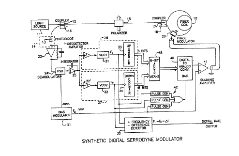
Figure 1 is a block diagram of the digital synthetic
serrodyne for fiber optic gyroscope, and
Figure 2 is another block diagram embodiment in many
ways similar to Figure 1.
Figure 3 shows symbolic waveforms of the digital
outputs of the up counter, the down counter and the adder means
of Figure 1.
6
64159-1159 ca o20203~9 2000-o6-of
Figure 4 comprising Figs. 4a, b and c is an
electrical schematic diagram of portions of the block diagram
of Figure 1.
DESCRIPTION
In the digital synthetic serrodyne for fiber optic
gyroscope of this invention there is a simplification of the
system block diagram in that the output signals of the "up"
counter and of the "down" counter of the positive and negative
serrodyne generators, respectively, are connected to inputs of
adder means. The output of the adder means is connected to a
high speed digital-to-analog converter (DAC) and then to an
amplifier having its output connected to drive the phase
modulator. The advantages of this improved circuit include
that only one high speed DAC and AMP are required. This gives
6a
~~2~3~~
faster reset times than any analog duplex or analog
synthetic single serrodyne. Also it is all digital
except for the phase sensitive demodulator, integrator
and DAC.
Referring now to Figure 1 there is shown a
system diagram of a fiber optic gyroscope system
according to the invention. A fiber optic coil 10 is
wound on a spool with a typical length of the optical
fiber coil on the order of 100 meters to 2000 meters.
Electromagnetic (light) waves which propagate in
opposite directions through coil 10 are provided from
a light source 11. This light source is typically a
broad-line width (a~a 20 nm) superradiant
(sometimes called superluminescent) diode, typically
emitting in the near-infrared portion of the spectrum
(for example at a wavelength of 830 nm to 1500 nm).
Between light source 11 and fiber optic coil
10 there is shown an optical path arrangement formed
by an extension of the ends of coil 1o to several
optical coupling components 12, 13, 14, 15, 16, 17, 18
and 20 to be described below. A portion of the same
kind of polarization-maintaining optical fiber as in
coil 10 is positioned at source 11 to receive the
light emission therefrom and extends to a first port
of an optical directional coupler 12. Optical
directional coupler 12 is of a type which has four
ports, two on each end. At the other port on the same
_7_
end of the coupler 12 there is shown a further optical
fiber positioned against it and which extends to be
positioned against a photodiode 13 which is
electrically connected to a photodiode system 14. The
photodiode 13 detects the light waves impinging
thereon from the adjacent optical fiber and
propagating from the coupler 12, and provides a
photocurrent, which is a function of the impinging
radiation.
Optical directional coupler 12 has another
optical fiber against a port at the other end thereof
which extends to a polarizer 15. At the other port on
that same side of coupler 12 there is a nonreflective
termination 16 including another portion of an optical
fiber.
Directional optical coupler 12 in receiving
light waves in any of its ports transmits such light
so that approximately half appears at each of the two
ports of coupler 12 on the end thereof opposite that
end having the incoming port. No light is transmitted
t~ the port which is on the same end of the coupler 12
as is the incoming light port.
Polarizer 15 has a port on either end thereof
with light transmission media continued therein.
Positioned against the port on the opposite end
thereof opposite that connected to optical directional
coupler 12 is another optical fiber portion which
_g_
r
2~2~3~~
extends to a further optical bidirectional coupler 17
which has the same light transmission properties as
does coupler 12.
The other port on the same end of coupler 17
from which a port is coupled to polarizes 15 is
connected in a non-reflective termination 18 using a
further optical fiber sectiAn. Now turning to the two
ports on the other end of coupler 17, one is directly
coupled to one end of the optical fiber in coil 10.
The other port is connected to a phase modulator 20 in
the optical path extending to the other end of the
optical fiber in coil 10. The phase modulator 20 has
two ports, one on either end of transmission media
contained therein. The optical fiber from coil 10 is
positioned against one port of phase modulator 20 and
the optical fiber extending from coupler 17 is
positioned against the opposite port to complete the
optical path followed by light waves from source 11.
The phase modulator, loop coupler and polarizes can
zp take the form of a multifunction integrated optic chip
if desired.
Phase modulatar 20 is capable of receiving
electrical signals from the phase difference
controller to cause it to introduce a phase difference
z5 in light transmitted therethrough by changing the
index of refraction of the transmission media therein
to change the optical path length.
-9-
~~2fl~~9
In operation, the light from source 11 is
coupled through the optical fiber portion to optical
directional coupler 12. Some of that light entering
coupler 12 from source 11 is lost in non-reflective
terminating arrangement 16, but the rest of that light
is transmitted through polarizer 15 to optical
directional coupler 17. Coupler 17 serves as a
beam-splitter in that the light entering the port
thereof received from polarizes 15 splits in half with
one portion thereof passing out of each of the two
.ports on the opposite end. From the one port light
passes through coil 10, through modulator 20 and back
to coupler 17. There a portion of that returning
light is lost in non-reflective arrangement 18, but
the rest of that light passes through the other port
of coupler 17 to polarizes 15 and to coupler 12 where
a portion of it is transmitted to photodiode 13. The
other part of the light from beam-splitter 17 leaving
the other port thereof passes through modulator 20 and
coil 10 to reenter coupler 17 and, again with a
portion thereof following the same path as before the
other portion to finally impinge on photodiode 13.
Photodiode 13 provides an output photocurrent
proportional to the intensity of the two light waves
impinging thereon to the phase difference controller
circuit. The output photocurrent depends on the
resulting optical intensity of the two waves incident
-10-
~~2~~'~~
on photodiode 13, which intensity will vary depending
on the degree of constructive or destructive
interference which occurs between the two light
waves. This interference of waves will change with
rotation of the coiled optical fiber 10 about its axis
as such rotation introduces a phase difference between
the waves.
The remainder of Figure 1 shows in block
diagram form a novel electrical system portion which
forms a phase difference controller feedback loop from
photodiode l3 to the optical path at optical phase
modulator 20. Thus the output signal from
photodetector system 14, including photodiode 13 is
provided to a transimpedance amplifier 22, where it is
amplified and passed to a phase sensitive demodulator
(PSD) 24 serving as a phase detector. The PSD
provides an indication of the relative phase of light
waves impinging on the photodiode 13. Integrator 25
receives the output of PSD 24 and stores all error
excursions at the output of the PSD and provides a
countering output signal based upon the time integral
of those errors. The integrator output signal causes
a sufficient phase shift in the optical path through
modulator 20 to provide zero error, or zero phase
difference in the steady state resulting from a
constant rotation rate.
-11-
f
2~~~3'~9
The output signal from the integrator 25 is
applied to the inputs of a positive serrodyne
generator 26 and a negative serrodyne generator 27.
The generator 26 comprises a voltage controlled
oscillator (VCO) 31 and an "up" counter 33. The
generator 27 comprises an inverter 32~, a voltage
controlled oscillator 32 and a "down" counter 34.
Initial frequencies of both of the VCO's may be at 15
MHz, for example. The output F1 of VCO 31 and the
output F2 of VCO 32 are fed to the input of a
frequency difference detector 30 which provides a
digital rate output OF = F1 - F2. Output F1
is also connected to the input of "up" counter 33 and
input F2 is connected to the input of °'down" counter
34.
The output of the two counters 33 and 34 is
connected to the inputs of an 8-bit adder means 35.
The adder means may comprise an adder or may comprise
an adder #1 followed by an adder #2. The output of
the adder means is connected to a digital-to-analog
canvert~r (DAC) 40. The output of the DAC 40 is
connected through an amplifier 41 to the phase
modulator 20. The bias modulator 21 provides proper
signals to tha PSD 24 and to the adder #2. If adder
#Z is not included then the bias modulator signal is
instead summed at summing amplifier 41. A strobe
-12-
~~ ~~~'~9
circuit 42 is connected to the DAC 40 to strobe the
DAC anytime a transition occurs.
The operation of the electrical circuit
operates as follows. The output of the integrator 25
which is nonzero when the gyro is rotated, is fed with
opposite polarity to VCO 32 compared to VCO 31. This
results in VCO 31 outputting a higher frequency than
VCO 32. Thus counter 33 counts sequentially up faster
than counter 34 counts sequentially down. The binary
words out of the counters 33 and 34 (,yu(t),
~d(t)) are applied to adder #1. The output of
adder #1 (~ri(t)) is summed with the binary
square wave modulation (~pb(t)) in adder #2. The
output of adder #2 (~r2(t)) is converted in the
digital-to-analog converter 40 to the analog serrodyne
signal X63 (t) . Amplification is normally
required with the more customary serrodyne signal
,y(t) being applied to the phase modulator 20.
Loop closure obtains since a phase ramp with the
proper slope is applied.
Referring now to Figure 3 there are shown
symba~lic waveforma of the up-counter 33 digital
output, the down-counter 34 digital output and the
adder 35 digital output into the digital-to-analog
converter (DAC) 40. The waveforms are referred to as
symbolic because it will be appreciated that the
serrodyne signals are digital words until the final
-13-
v
~~~~3'~~
digital to analog conversion. The equivalent analog
signal is shown for representation only. In actuality
the up and down counters may preferably be 8-bit (or
higher) counters, however in the representative
waveforms A, B and C of Figure 3 a 3-bit digital
synthetic serrodyne system has been shown. Thus in
waveform A representing the "up" counter output, the
progressive eight bits in the count from 000 up
through 111 are shown and repeated five times. Tn
waveform H representing the down counter output, the
progressive eight bits stepping downward are shown and
repeated about three times. These two counter outputs
are added together in the adder means 35 and waveform
C represents the adder means digital output into the
DAC 40. It will be appreciated that the strobe
circuit 42 causes the DAC to convert anytime an event
occurs in the VCO's or bias modulation. This DAC
timing pulse, which is necessarily of short duration,
strobes the DAC the minimum times needed in order to
prevent extra DAC glitches.
Figure 2 shows an embodiment having two
adders with the outputs of the counters 33 and 34
feeding the adder #1. The output of the adder #1
feeds one input of adder #2 and a bias modulation
signal is inputted to the other input of adder #2,
however, it is possible to eliminate adder #2 and the
digital squarewave modulation. Then the bias, which
-14-
2~~03~9
can be sinusoidal or squarewave is summed into the
amplifier 41 as shown in the embodiment of Figure 1.
This bias modulation can be applied in several
equivalent ways using our basic approach.
Figure 4 comprising Figs. 4a, b and c is one
example of a schematic diagram of part of the
electrical portion of the block diagram of Figure 1.
Figure 4 includes a schematic of the VCO1 and VC02,
the up counter 33, the down counter 34, the 8-bit
adder 35, the digital-ta-analog converter 40 and the
,summing amplifier 41. Each of these sections of the
circuit has been outlined with dashed line enclosures
and numbered the same as in Figure 1.
The invention disclosed herein has a number
of advantages including:
a) Optimum reset time is achieved since only
one ap-amp (amplifier) is needed.
b) The digital approach is easier to
productize since application specific integrated
circuits can be applied. Cast and reproducibility
issues are favorably affected.
c) Gyro bias and bias stability errors are
not generated because baseband frequency shifting
is employed.
d) There are no dynamic response problems at
low rates since the novel digital waveform
provides smooth baseband operation.
-15-
f
2~~~~~~
e) The single modulator design eliminates
imperfect aging or temperature tracking problems
associated with two modulators.
f) The applied frequency count indicates the
applied rate to the gyro.
g) If a 2~ phase deviation servo is
required, a single servo loop suffices.
h) Bias modulation can be simply added
either digitally (square wave modulation) or by
analog (sinusoidal modulation) methods.
ao
-16-
s