Note: Descriptions are shown in the official language in which they were submitted.
2~204~6
.
DUAL DOMAIN MEMORY CONTROLLER
Background and Summary of the Invention
The present invention relates to memory controllers for use in
microcomputer systems incorporating commercially available microprocessor
chip sets. In particular, this invention relates to microcomputers in which
an asynchronous memory controller is used to access the system memory
asynchronously with respect to the operational speed of the microprocessor
chip set. Memory controllers generally provide control signals for writing
data to and reading data from system memory.
Microprocessor and memory chip sets are advancing rapidly and are
expected to continue to advance indefinitely. Moreover, microprocessor and
memory chip sets are advancing at different rates so that the difference in
performance parameters, particularly operational speed, of the microproces-
sor, the memory and the bus over which they typically communicate tends
to expand or contract, i.e., become greater or lesser, as advances are
~; perfected. In addition, performance characteristics of microcomputers chip
sets employing emerging technologies also advance at different rates.
While present-day microcomputer manufacturers have control over the
design and configuration of the systems they produce, they typically must
anticipate the parameters necessary for compatibility of their system with
,.. ~ . .
new microprocessors and memory devices, as well as add-on peripherals,
accessories and memory options produced by other manufacturers. The
performance and interface characteristics of microprocessors and memory
devices often vary substantially from one release of the same device to the
next; sim~larly suchlcharacterisitics of peripherals, accessories and memory
options~will vary among the manufacturers of these devices.
While the performance characteristics of peripheral devices are often
designed for less than optimum performance, i.e., "detuned" to accommodate
variation, in microcomputer system designs, microprocessor chip and
memory devices are not usually so detuned. Therefore, the manufacturer of
,,., .~
2020~56
.
high performance microcomputers much allow for different, even inferior,
performance characteristics of peripheral and accessory devices and some
memory options in order to produce a system which is compatible with the
maximum number of devices attachable to the system. In addition, the
5 microcomputer manufacturer must anticipate upgrades and changes of
microprocessor chip sets and memory devices. If the microcomputer
manufacturer does not so anticipate such upgrades, it will limit the
marketability of the system to less than the total market available for his
product.
A complete microcomputer, which is often intended for desktop
applications, includes subsystems such as a central processing unit (hereafter
referred to as the "CPU", "processor" or "microprocessor"), a math "coproce-
ssor", DMA capabilities, memory, miscellaneous system ports, and interfaces
to video, keyboard, floppy disks, serial and parallel ports, scsi devices, and
15 a mouse pointing device.
The microcomputer functions by manipulating address, data, and
control signals among the subsystems within the system. The control data
flow into and out of system memory is provided by a memory controller
which usually controls the data flow and timing between the processor, main
20 system memory, and the bus.
As faster microprocessor and memory devices became availableto
microcomputer system designers, increased performance was limited by other
components of the systems. For example, the speed of memory controller
technology could not be expected to increase at a rate commensurate with
the inçreasing speed of the microprocessor and memory devices, especially
as the relative operation of microprocessors and memory devices is changed
and changed at different rates.
7 ''~ If the memory controller were simply driven faster to take advantage
o f the faster microprocessors and memory devices now becoming available,
30 certain~ memory devices would begin to fail in different ways in different
7": :
systems. The faster the memory controller is driven to keep pace with
~ ~ .
,;.
". ~
2020~6
, . . .. .
microprocessors, the more memory devices would fail and start to fail.
Failure modes include loss of data, and loss of address and control signals.
Therefore, a microcomputer system which incorporates faster microprocessor
technologies, e.g. 20 or 25 MHz, slower memory device technologies, and still
slower inputloutput (VO) bus technology, e.g., operating at 8 MHz, is
extremely desirable.
While development of memory components such as Dynamic Ran- dom
Access Memory ("DRAM") devices have usually kept pace with processor
technology, often the control logic for these devices does not. Such logic
functions and technology were also a limitation on overall microcomputer
system speed. For example, in order for the processor to access memory,
access signals must be produced in response to bus controller strobe signals
which, in turn, are produced in response to access request signals from the
micro- processor. Additive overhead associated with both the bus and
memory controllers arising from buffering and gate delays is required to
produce these signals. Thus, the need is clear for system memory control to
be dissociated from the speed of advancing microprocessor technology on the
one hand and from conventional or state-of-the-art bus/bus controller
technology on the other, not withstanding the high degree of interaction
between the processor and system memory.
The speed of operation of microcomputer subsystems is governed by
one or more clock or timing signals which may or may not be synchronized
In the pas~, such clock signals were usually derived from more than one
source which was not synchronized. Thus, when synchronized operation
of the mlcroprocessor and~systfm memory was required, tolerances in jthe
timing of control, gating and handshake signals had to be relaxed enough
to allow for imprecise cooperation of clock signal source. For microcom-
puters operating at 8 MHz, performance was acceptable and reasonably
reliable.
As operating speed is increased, however, critical system timing
arameters must be substantially more precise than can be reliably achieved
~
~ 2020~56
with multi-source clock signals. Thus, for operation at 20 MHz and above,
clock signals produced from one source are required to preclude clock and
control signal skewing and provide reliable, high-speed operation.
System memory control according to the present invention comprises
a synchronous controller for interface with the microprocessor of the
designer's choice and an asynchronous memory controller for direct interface
with present state-of-the-art input/output (VO) bus technology such as the
Micro Channel Architesture (MCA) manufactured by IBM Corporation.
Thus, accessing of 80 nanosecond DRAM available from any number of
manufacturers, by either the controller of the present invention, high-speed
microprocessors or bus-coupled devices in a microcomputer, bus timing
system having enhanced performance characteristics is facilitated. By
dividing system memory control according to the present invention, the
evolving technologies of microprocessors and DRAM are anticipated and
neither are hampered by the speed of the MCA or pace of development or
nature of other conventional bus technology. It is also desirable to have
asynchronous memory controller technology for access to memory by bus
coupled devices without impacting, i.e., detuning, the performance of either
the microprocessor or system memory.
The asynchronous control unit of the present invention provides bus-
coupled devices with asynchronous access to a microcomputer system
memory in response to control signals from the main YO bus. Synchronous
memory controllers are well known for providing the microprocessor access
to system memory in response to command signals from the microprocessor
~ The present invention may be used to enhance the performance characteris-
tics of the overall microcomputer system by providing separate access to
memory for devices and subsystems coupled to the main VO bus at speeds
different from those required by high performance microprocessors. Thus,
with the control unit with the present invention, buffering, control signal
conditioning or other additive overhead previously required for access to and
from system memory by VO bus coupled devices via a synchronous memory
20204~6
controller is eliminated. Meta stability problems on the boundary of the
synchronous and asynchronous domains are also eliminated.
Description of the Drawing
Figure 1 is a block diagram of a memory control system employing an
asynchronous memory control unit constructed according to the principles `
of the present invention. ~
Figure 2 is a block diagram of the asynchronous memory con- trol unit ;
employed by the memory control system of Figure 1.
Figure 3 is a timing diagram for control signals produced by the asyn- ~;
chronous memory control unit of Figures 1 and 2.
Description of the Preferred Embodiment
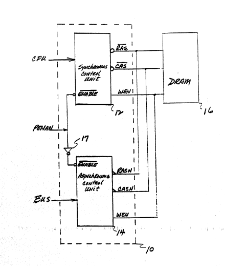
Referring now to Figure 1, memory control system 10, according to the
present invention, comprises synchronous control unit 12 and asynchronous ~ ~ -
control unit 14. Control units 12 and 14 each produce row and column
address (RAS and CAS, respectively) signals and a write enable (WEN) signal
for accessing Dynamic Random Access Memory (DRAM) 16. The designa-
tion for RAS and CAS signals, as well as other signals described herein, may
also indude a suffix N, such RASN and CASN. Such designation is used
merely to indicate that such signals are active at low voltage or negative
polarity.
Synchronous Control Unit 12 be any commercially available memory
controller suitable for producing RAS, CAS and WEN signals response to
commands from a m~icroprocessor, such as the synchronous GC182 M,emory
Controller produced and marketed by G2 Incorporated. DRAM 16 may be ~ -
any commercially available DRAM devices, preferably having high speed
performance characteristics suitable for receiving RAS, CAS and WEN signals
produced by synchronous unit 12. Such DRAM devices include the HM
5110003 and the MB 81C1000 80 NS devices manufactured by Hictachi and
FuJitsu, respectfully. ~ - -
',` ~ .~ ~' .'-
2~20~56
Asynchronous control unit 14 produces RAS, CAS and WEN signals
31, 32 and 33 (as shown in Figure 3), respectively, in response to control
signals from the main VO bus. In the preferred embodiment of the present
invention, asynchronous control unit 14 is designed to receive control signals
produced by and for interfacing with the MCA bus as described in the
Technical Reference manual for the IBM Personal System/2 microcomputer
which is incorporated by reference as if fully set forth herein.
5ynchronous control unit 12 and asynchronous control 14 are both
enabled by the PENA~N signal. PENAN is low (i.e. negative) when synchron-
ous control unit 12 is enabled; PENAN is high (i.e. positive) when asynchro-
nous control unit 14 is enabled. Thus, both controllers are never enabled at
the same time.
The state of the PENAN signal is determined by the microprocessor. If
an 80386 microprocessor chip, produced by Intel, Inc., is used, PENAN is
derived from the HOLDACK signal produced by the microprocessor in
response to a microprocessor hold request signal. Thus, when the microproc-
essor controls the MCA bus, synchronous unit 12 is used to access DRAM
16. Conversely, when the microprocessor does not have control of the MCA
bus, asynchronous controller unit 14 is used to access DRAM 16.
S~nchronous control unit 12 is typically a high speed controller
operating in the 25 to 33 MHz range, having zero wait shtes and 40
nanosecond cycle times. In contrast, asynchronous control unit 14 is slower~
speed system, operated typically on 200 nanosecond memory cycle time.
Inverter 17 assures that asynchronous control unit 14 is never enabled at the
same time synchronous control unit 12 is enabled.
Referring now to Figure [3], asynchronous control unit 14 comprises
gates M100-M102, M105-M112 and flip-flops M103-M104.
Asynchronous control unit 14 produces RAS, CAS and WEN signals response
to the logical combination of MCA signals CMD, Refresh, CRAMCS, SO and
S1, DELCMD, and CADL, as described elsewhere in this specification.
DELC2~ID is a delayed version of MCA signal CMD, and CRAMCS is an
- `
20204~6
address and status decode signal from the MCA which indicates a memory
access.
Referring now to Figure 2, asynchronous control unit 14 produces WEN
signal 33 in response to SON and SIN according to the relation
WEN = SON' NAND SIN,
where SON' is the complement of SON. SON and SIN signals are clocked
by CMDN signal becoming active, i.e. low, via clocked latches M103 and
M104.
With continuing reference to Figures 2 and 3, asynchronous control
unit 14 produces RASN signals 31 in response to CADLN or REFRESHN
signals becoming active. RASN remains active until, and becomes inactive
(i.e., high) when, OR gate M111 opens in response to DELCMDN becoming
active (i.e., low).
CASN signal is produced by 4-input NAND gate M101 when CMDN
becomes active in the presence of several other MCA signals according to the
relation
CASN=[[SON XOR SIN] ~ CRAMCS ~ REFRESHN ~ CMDN']', :
where CMDN' is the complement of CMDN. The function [SON XOR SIN]
is produced by XOR gate M102, and CMDN' is produced by inverter M100.
As indicated in Figure 1, in the preferred embodiment, the output ports
of asynchronous control unit 14 are wire-ored with the output ports of ~ -synchronous control unit 12 at the input ports of DRAM 16. Similarly the
WEN signal port of asynchronous control unit 14 is wire-ored with the
analogous port of synchronous control unit 12 at the write enable port
25 DRAM 16. This configuration is facilitated by the tri-state signals produced ;
by the bi-cmos components of asynchronous control unit 14.
- :,
:
: :