Note: Descriptions are shown in the official language in which they were submitted.
t sl ~i~ t,) '9
BACKGROUND OF THE IN'~IENTION
Field of the Invention
The present invention -relates generally 'to television
receivers and, more particularly, is directed to an automatic
fine tuning (AFT) circuit for use with a television receiver in
which the AFT operation can be readily pulled in.
Description of the Prior Art
As a channel selecting apparatus of, for example, a
television receiver, a synthesizer tuner having a phase locked
loop (PLL) circuit is utilized frequently. Such synthesizer
tuner can stably receive a television signal if the frequency
of a television signal is inherently accurate.
Recently, it is frequently observed that the frequency of
an RF (radio frequency) signal in the re-transmission of
television signal in a so-called CATV, a video tape recorder
(VTR), a -television game machine or the like is offset from the
original frequency. Further, in the CATV, in order to avoid
the disturbance from the adjacent channel or the like, the
frequency of RF signal is offset from the original frequency by
about 1 MHz.
Therefore, it is proposed to provide a so-called automatic
fine tuning (AFT) circuit in the synthesizer tuner to pull-in
the receiving signal having an affse-t frequency (see U.S. Pat.
No. 4,422,096). Further, Japanese Patent Laid-Open Gazette No.
63-174433 describes a wide AFT in which the AFT operation is
sequentially carried out at five to six channel-selection
points within a channel so as to substantially widen the range
in which the AFT operation is pulled-in.
In the above-described AFT circuit, in the stationary
state, an AFT signal detecting- period is restricted within
_1-
b g~ c, ~ ~-y ~~ ~?
s~~~~~Cy~3
only a vertical blanking period, whereby a fluctuation in which
an AF'T signal is fluctuated by the level change of a video
signal is removed, thus the AFT operation being stabilized (see
Japanese Patent Laid-Open Gazette No. 63-135075).
However, under the condition that the synchronization of a
receiving signal is not estabished such as when a television
channel is selected, the vertical blanking period of the
receiving signal and an AFT detecting period, determined at the
television receiver side, are not coincident: with each other.
In that case, if the receiving signal is a video signal of
normal level, a satisfactory AFT control signal is obtained in
other period than the vertical blanking period.
If, for example, the receiving signal is a video signal
having high average picture level (APL), the level of an IF
(intermediate frequency) signal is lowered during the video
signal period sa that the level of the .AFT signal is lowered.
Consequently, an AFT signal of sufficiently high level can not
be obtained only in the detecting period in which the receiving
signal is not synchronized. There are then the substantial
disadvantages that a mal-function will occur and that the AFT
operation is pulled in with plenty of time.
OBJECTS AND SUMMARY OF THE INVENTION
Accordingly, it is an object of the present invention to
provide an improved AFT circuit which avoids the aforenoted
shortcomings and disadvantages of the prior art.
More specifically, it is an object of the present
invention to provide an AFT circuit in which an AFT operation
can be pulled in rapidly and positively.
As an aspect of the present invention, at least during a
channel selection period, an AFT detecting period is made
_2_
()
~~~~~.,~~~~r
longer than one vertical scanning period, and after the AFT
operation is pulled in, the AFT detecting period is restricted
within the vertical blanking period. Accordingly, at least
during the channel selection period, the AFT de~Lecting period
is made longer than one vertical scanning period, whereby the
detection of AFT signal can be carried out positively. Thus,
the AFT operation can be pulled in satisfactorily and rapidly.
The above, and other objects, features arid advantages of
the present invention, will be apparent in the following
detailed description of a preferred embodiment of the invention
when read in conjunction with the accompanying drawings, in
which like reference numerals are used to identify the same ox
similar parts in the several views.
BRIEF DESCRIPTION OF THE DRAWINGS
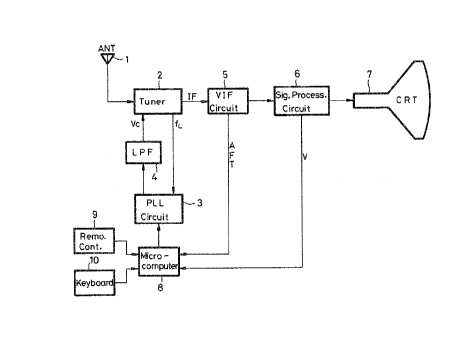
Fig. 1 is a block diagram showing an embodiment of an AFT
circuit according to the present invention; and
Fig. 2 is a flow chart to which reference will be made in
explaining an operation of the AFT circuit shown in Fig. ~..
DETAILED DESCRIPTION OF THE PREFERRED EMBODIMENT
An embodiment of an automatic fine tuning (AFT) circuit
according to the present invention will be described with
reference to Figs. 1 and 2.
Fig. 1 is a schematic block diagram of a television
receiver to which the present invention is suitably applied.
It will be seen in Fig. 1 that a television signal is
received at an antenna l and this received signal is supplied
to a tuner 2. The tuner 2 is also supplied with a channel
selection voltage Vc produced by a phase locked loop (PLL)
circuit 3 and a low-pass filter (LPF) 4 and, a local
oscillation signal ft from the tuner 2 is supplied to the PLL
-3-
S j~ G. ~~
. ,,~ ~~ ~,.t '~ 5
~J t J i.Y L) f'.,~ C
circuit 3.
Thus, a desired television signal is received on the basis
of a numerical value set in the PI,L circuit 3. The received
signal IF from the tuner circuit 2 is supglied to a video
intermediate frequency (VIF) circuit 5 including a video
detector circuit, and the demodulated video signal from the VIF
circuit 5 is supplied through a signal processing circuit 6 to
a cathode ray tube (CRT) ?, whereby a desired television signal
is reproduced on the CRT 7 as a picture.
A microcomputer 8 receives control signals from a remote
control circuit 9 and a keyboard 10 and generates a pre-
determined numerical value in order to receive a desired
television signal. This numerical value is set in the Phh
circuit 3.
Further, the VIF circuit 5 derives an automatic fine
tuning (AFT) signal. This AFT signal is supplied to the
microcomputer.8, and a vertical sync. (i.e., synchronizing)
signal V separated from the video signal by, for example, the
signal processing circuit 6 is supplied to the microcomputer 8.
Accordingly, in this circuit arrangement, in the
stationary state, on the basis of the vertical sync. signal V
from the signal processing circuit ~, the AFT signal is
detected during a vertical blanking period and the AFT signal
is controlled to have a predetermined level. Thus, the AFT
operation is performed.
In the channel switching mode, a different operation is
performed by the microcomputer 8.
The overall AFT operation of this invention is represented
in the flow chart forming Fig. 2. In Fig. 2, step 20, steps 39
to 42 and steps 44, 45 are executed in the prior art and steps
-4-
4 ~o~~cofa~w
i~~ ~~ ~.f iW
21 to 38 and 43 are additionally executed in the present
invention.
Referring to Fig. 2, switching ON the power switch of the
television receiver' and following the Start of operation, it is
initially determined in decision step 20 whether or not the
self-oscillating vertical sync. signal in the signal processing
circuit 6 goes to "0" from "1". If a NO is output at step 20,
this means other portion than the front edge portion of the
vertical synchronizing signal. Then, the routine goes to step
21, whereat the AFT signal from the V'IF circuit 5 is taken in.
It is determined in the next decision step 22 whether or not
the signal taken in is a signal which increases (UP) a
reception frequency. If a YES is output at step 22, then the
routine proceeds to step 23, whereat a count value [DN] for
counting the number of a down (I3N) signal, which will be
described later, is reset to "0". In the next step 24, a count
value [UP] far counting the number of up signal is incremented
by "1". It is determined in the next decision step 25 whether
or not the count value [UP] is larger than "7". If the count
value [UP] is larger than "7", as represented by a YES at step
25, then the routine proceeds to step 2~, whereat the UP flag
is set to "1", and the routine returns to step 20. If the
count value [UP] is not larger than ""7", as represented by a NO
at step 25, then the routine directly returns to step 20.
If it is determined that the AFT signal is riot the UP
signal, as represented by a NO at step 22, the routine proceeds
to step 27, wherein the count value [UP] is reset to "0".
Then, in the next decision step 28, it is determined whether
the AFT signal. taken in is a signal which decreases (down} the
reception frequency or not. If the AFT signal is the down
_.5.-
;>
'~t,~ FJ 1i~ lh C:)
signal, as represented by a YES at step 28, then 'the routine
proceeds to step 29, whereat the count value [DN] is
incremented by "1". The processing proceeds to the next
decision step 30, whereat it is determined whether or not the
count value [DN] is larger than "7". If the count value [DN]
is larger than "?", as represented by a YES at step 30, the
routine proceeds to step 31, whereat the DN flag is set to "1",
and the routine returns to step 20. If the count value [DN] is
not larger than °'?", as represented by a NC> at step 30, then
the xoutine directly returns to step 20.
If the identified AF'f signal is not the down (DN) signal,
represented by a NC) at step 28, then the count value [DN] is
reset to "0" at step 32, and the routine goes back to step 20.
On the other hand, if it is determined that the vertical
sync. signal goes to "0" from "1", as represented by a YES at
step 20, this means the front edge portion of the vertical
sync. signal. Then, the routine proceeds to the next decision
steps 33 and 34, whereat the UP flag and DN flag are
identified. If any one of UP and DN flags is "1", the
corresponding up (UP) or down (DN) operation is executed at
step 35 or 36. The up and down operations at steps 35 and 36
are wide automatic fine tuning operations described in the
preamble (prior art) of this specification.
At the completion of the steps 35 and 36 or if the UP flag
and the DN flag are both "0", as represented by a YES at steps
33 and 34, then the routine proceeds to the next decision step
3?, wherein it is determined whether or not the AFT signal is
pulled in completely. If the pull-in operation of the AFT
signal is not completed, as represented by a NO at step 3?, the
routine proceeds to step 38, whereat the UP flag, DN flag and
_6_
~3 ~1 f~ ~i ~
'ty t.i L% C:
count values UP and DN are all reset to "0", and the routine
returns to step 20.
If the pull-in operation of the AFT signal is completed,
as represented by a YES at step 37, the routine proceeds to the
next decision step 39, whereat it is determined on the basis of
the vertical sync. signal from the signal processing circuit 6
whether or not the AFT detecting period is within the vertical
blanking period. At a timing point in which. the pull-in
operation of the AFT signal is completed, the vertical sync.
signal from the signal processing circuit 6 is synchronized
with the reception signal. If the AFT detecting period is not
restricted within the vertical blanking period, as represented
by a NO at step 39, the step 39 is repeated.
If the AFT detecting period falls within the vertical
blanking period, as represented by a YES at step 39, the AFT
signal is taken in at step 41. Then, in the next decision
steps 41 and 42, it is determined whether or not the UP signal
and the DN signal exist. Further, it is determined at the next
decision step 43 whether or not the channel select command is
issued. If neither the UP signal and the IAN signal exist nor
the channel select command is issued, as represented by a NO at
steps 41, 42 and 43, the routine returns to step 39.
If the AFT control signal exists in any one of the two
steps 41 and 42, as represented by a YES, then the routine goes
to steps 44 and 45, whereat the corresponding up and down
operations are performed, and then the routines return to step
39. Further, if the channel select command is issued, as
represented by a YES at step 43, the routine proceeds to step
38.
The above-mentioned processings at steps 39 to 43 and .
a
~~~'~;;~~'~ a
steps 44 and 45 are executed in 'the stationary state. In the
stationary state, these steps 39 to 43 and steps 44 and 45 form
an infinite loop and these operations are stopped by turning
OFF 'the power switch and the like.
Accordingly, in the flaw chart of Fig. 2, upon channel v
selection, for example, the loop formed of steps 20 to 32 is
repeated to successively detect the AFT signal, which is
detected at a timing of the self-oscillating vertical sync.
signal from the signal processing circuit 6. Therefore, during
this identification, the detection of the AFT signal is
continuously carried out substantially over one vertical
scanning period and the vertical blanking period of the
reception signal is always involved in one vertical scanning
period. Thus, even if an average picture level (APh) of the
video signal is so high that the AFT signal of the vertical
scanning period can not be obtained, the AFT signal can be
positively detected by the signal within the vertical blanking
period.
At step 21 in the flow chart forming Fig. 2, the AFT
signal can be taken in at the interval of, fox example, 100 x
10-6 second in the above-mentioned loop. In that case, only
when the AFT signal contains more than successive seven up or
down signals, the UP flag or the DN flag is set to "1", whereby
a mal-function due to the noise component in the signal or the
like can be avoided.
As set out above, according to the above-mentioned circuit
arrangement, at least during the dhannel selection period, the
AFT signal detecting period is made longer than one vertical
scanning period, whereby the AFT signal can be detected
positively. Thus, the AFT operation can be pulled-in
_g_
'~ 4..h ~"r ~.
t; i.3 Cdr P
satisfactorily in a short period of time.
zn the flow chart forming Fig. 2, the decision at step 20
may be executed not by the vertical sync. signal but by a timer
driven in an interval of longer than 1G.7 x 10-3 second.
Having described a preferred embodiment of the invention
with reference to the accompanying drawings, it is to be
understood that the invention is not limited tothat precise
embodiment and that various changes and modifications could be
effected by one skilled in the art without departing from the
spirit or scope of the novel concepts of -the invention as
defined in the appended claims.
_g_