Note: Descriptions are shown in the official language in which they were submitted.
CA 02020856 1999-04-07
COMPOSITE OXIDE THIN FILM
The present invention relates to a composite oxide
thin film, and more particularly, to a composite oxide
thin film formed through an electrochemical reaction and
a water thermal reaction.
Composite oxide thin films are attracting the
general attention as electronic materials for various
applications and have already been industrialized or
subjected to trial manufacture in different manners as
materials for an inductor, a sensor, an optical
component, a magnetic use and superconducting
application.
There have conventionally been known, as such
composite oxide thin films, ones formed by physical
evaporation as typically represented by sputtering and
ones formed by chemical evaporation as typically
represented by CVD and MOCVD. These conventional
composite oxide thin films based on vapor synthesis
involve some problems to be solved.
More specifically, these films based on vapor
synthesis are defective in that they have a low rate of
growth of the film and require consumption of much
energy. In these methods, easy occurrence of non-uniform
evaporation and the reaction under a low partial oxygen
pressure tend to cause such oxygen demand, leading to the
possibility of being converted into semiconductors, thus
needing annealing after film formation. During annealing,
however, the substrate and the composite oxide thin film
may react, or peel off may be caused.
The low insulation fracture voltage relative to the
film thickness is another problem.
- 1 -
CA 02020856 1999-04-07
In the case of the CVD method, a raw material of a
high volatility must be used, but such a raw material is
usually unstable and difficult to handle, with a very
high cost.
In addition to these vapor phase method, there are
known several thin film forming methods based on the
liquid phase process, including, for example, a method
for forming a dielectric thin film by causing an electro-
chemical reaction through immersion of titanium of
zirconium in a molten salt of barium or strontium
(Japanese Patent Publication No. 43-2,650 of January 30,
1968), a method of immersing titanium in a molten salt
(Japanese Patent Publication No. 44-13,455 of June 17,
1969), and a method for forming a BaTi03 film through a
chemical treatment in a strongly alkaline aqueous
solution of barium (Japanese Patent Provisional
Publication No. 60-116,119 of June 22, 1985).
In the methods using molten salt, however, it is
necessary to employ a very high temperature and an
expensive pressure vessel and contamination from the
vessel is inevitable. It is furthermore difficult to
precisely control the film thickness.
In the case of chemical treatments, the defects
include the low growth rate and the difficult control of
the film thickness, and in addition, there is a concern
about contamination from such mineralizers as sodium and
potassium. In addition to those mentioned above, the
organic metal application method is known. This method is
however defective in that the thermal decomposition
through firing of an organic metal compound applied to
the substrate at a prescribed temperature causes a
considerable shrinkage during the firing step and
- 2 -
CA 02020856 1999-04-07
produces cracks in the resultant composite oxide thin
film, and furthermore, evaporation and combustion of the
organic components make it difficult to achieve a dense
sinter. The reaction with the substrate during firing is
another problem.
The present invention was developed in view of the
circumstances as described above and has an object to
provide a new composite oxide thin film which solves the
drawbacks of the conventional thin films, can be
synthetically manufactured at a temperature lower than in
the conventional manufacturing methods, is uniform and
excellent in crystallinity, and easy to manufacture even
in the case of a large-area film.
According to the present invention, there is
provided a method of manufacturing a composite oxide thin
film, comprising the steps of:
(i) providing a work electrode and an opposite
electrode immersed in an electrolytic solution, the work
electrode comprising a first metal and the electrolytic
solution comprising at least one reactive component which
is reactive with the work electrode and contains ions of
at least one metal other than the first metal in the work
electrode;
(ii) energizing the work electrode at a solution
temperature of at least 100°C. and under a pressure of at
least saturated vapor pressure of the solution, thereby
reacting the reactive component with the work electrode
and forming a composite oxide thin film which contains
oxides of the first metal and the metal other than the
first metal.
According to a preferred embodiment, the work
electrode, the opposite electrode and the solution are
- 3 -
CA 02020856 2000-08-14
contained within a pressure vessel. Preferably, the work
electrode comprises a metal selected from the group
consisting of titanium, aluminum, niobium, zirconium,
hafnium, lead, tantalum and iron; titanium is
particularly preferred. The opposite electrode, on the
other hand, preferably comprises platinum.
According to another preferred embodiment, the
reactive component is selected from the group consisting
of barium hydroxide, strontium hydroxide, calcium
hydroxide and lithium hydroxide. Preferably, the pressure
vessel further comprises means for heating the solution.
The temperature of the solution in the pressure vessel is
preferably maintained within the range of from 100°C. to
374.2°C. Direct or alternating current is preferably
applied to the electrodes in an amount effective to cause
reaction of the work electrode and the reactive
component.
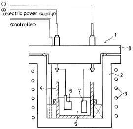
In the accompanying drawings:
Fig. 1 is a sectional view illustrating an
embodiment of the autoclave reaction apparatus applicable
when forming the thin film of the present invention;
Fig. 2 and 3 are chard diagrams illustrating the
results of X-ray diffraction for an embodiment of the
BaTi03 thin film of the present invention;
Fig. 4 is a chart diagram illustrating the result of
X-ray diffraction for the embodiment of the (Ba, Sr) Ti03
solid-solution thin film of the present invention; and
Fig. 5 is a chard diagram illustrating the result of
X-ray diffraction for the embodiment of the BaFe02,9 thin
film of the present invention.
The work electrode comprises a reaction-active mate-
rial such as metal, an alloy, an intermetallic compound,
- 4 -
CA 02020856 1999-04-07
or an inorganic substance. In this case, the work elec-
trode may be a single-body electrode or may be a compo-
site or a mufti-layer electrode, without any limitation
in shape; it may be of a special shape having, for exam-
s ple, a cavity, and the possibility of forming a composite
oxide thin film on the outer surface thereof or on the
inner surface thereof is one of the features of the
present invention. The work electrode may be formed on
- 4a -
FRUP7 W ?"77'J7T 6~v#a="4W 1999. 7.19 x:41 F. r
L~a ra c ~: rl r~"
,t1 ~ ~a~ JJ y~ ,;
the substrate comprising of inorganic materials, suoh as glass,
ceramics, and organic polymers.
Any axbi'~rary Oppo~irra Al.ao~rodo may be .u~e~l,
For the solution containing reactive components, any of
various chemica,i compositions may be adopted.
in general power should preferably be turned on under
pressurized and heating COtlditions in a pressure vessel. The
thin film of the present invention may be manufactured, for
example, in the apparatus as shown in Fig, 1,
In this embodiment, in the apparatus having a heater (3)
provided around an outer vessel (2) of an. autoclave (!) and an
inner vessel (4) such as one made of tephrorz provided in the
interior thereof, a work electrode; (6) and an opposite electrode
(?) are immersed in a solution (5) containing xeaoti,ve
components. A rid (8) is provided on the top of the outer
vessel (2) to clo$e the interior of the outer vessel (2).
xn such an apparatus, fox example, With a work electrode
(6) made of titaniura and an opposite electrode (T) made of
platinum, serving respectively as the anode and the ca~khode, a
BaTi03 thin film can be foamed on the surface of titanium by
energizing the electrod~:s in a barium hydroxide solution. Any
metal, $lloy or inorganic substance such as aluminum, niobium,
zirconium, hafnium, lead, tantalum or iron may be employed in
place of titanium. The solution (a) may contain any reactive
components reactive with the work electrode (6), including, for
example, barium hydroxide, strontium hydroxide, ca7.cium
hydroxide, and lithium hydroxide.
b _
FF,ut~1 _~~'I"~7~n( f~s~au~r.~a 195E~. 7.IE~ x:42 F. E~
-: c.; ~?, !i r f
6 ~. '
~~~~~~J~'.3
then a woxk electzode (6) made o:~ a metal is used as the
anode as deaaribed above, the metal of this, work electrode (6)
forma an oxide or begins to be solved into the-solution in the
state of anodic~oxidation, and reacts with the reactive
componerita in the solution (S), and composite oxides are
considered to be formed as a trcin film,
The temperature, the pressure and the applied eleatrio
current (DC or AG) ire the formation of the film, varying with
the xeaat.ion system, may be appropriately selected. P'or
example, the te~tpera,ture map be within the range of from 50°C to
the critical point c~f water (3~~4,2°C), and the pressure may be
at least the saturated vapor pressure, In the case of more low
temparture, axe autoclave is not necessary for the reaction.
Now, the present invention is described in more detail by
means of examples.
Example 1
A thin film was formed with the use of the apparatus shown
in Fig, 1, under the following condftlons:
Solution . 0.5 N - Ba(OTi) 2.8Fi20,
~lork electrode . Ti (pur.ity: 99.9%),
Oppasitr~ ele~etrode : Pt,
Temperature , 200°C,
Pressure . ~;aturated vapor pressure 2.0 mpa,
~leatxia current . 100 mA/em2 (DC).
~aTlO~ began to form on the surface of the work electrode.
The relat;lonshi.p between the applied ~roltagre and the
6 -
FROh1 _u7"~~~7?T f~~r~aW'4~a 19569. 7,19 9:4p F. 9
~.'~. ~ I~.
~t9 ~a ~~J C~ ~.:
treatment time is that the voltage shows a sudden initial rise,
and immediately after that, a constant value, with no remarkable
change thereafter. This is oonsidered attributable to the fast
that the gxowth.of the gilm and dissolution through aysthetic
reaoxion of the thin film aitnultaneoualy proceed" resulting in
equilibrium oP speeds.
The result of X-ray diffraction at the rea~ultant thin film
i9 illustrated in Fig. 2. The formed BaT103 was of a single
phase and had a satisfactory crystallinity.
example 2
A thin film ways farmed in the same manner as in the
Example 1 with a reaction temperature of 100°C. The result of X-
ray diffraction of the xeaulfiant BaT103 thin film is illustrated
in Fi,c~. 3.
Exam~lea 3 to 5
Thin films were formed in the same manner as in the
Example l, with.a concentration of 0.25 ~ of the soluti4n and a
current density of 50mA/cn2 while changing the temperature from
200°C to 250°C and 100°C.
fihe formation of the BaT303 thin film brought about, agtcr
the lapse of 30 minutes, the following changes 3n weight of the
work e.leCtrode:
200°C . 4,6 x 10⁻⁶ g/(cra2.minute)
150°C : 4.3 x 10-~' (cm2~minutey
100°C : 2.& x 14 G (cm2.minute)
- T
FROM W 'I"77~r~f F~s*sW'4~a 1'397. 7.13 9:4:, F.1~J
Lxample 6
A ~aTi03 thin film was farmed an a titanium sheet h$ving a
thickness of 1.0 mm by changing only the following conditions:
Solution ~ . 0.25N - Sa(pH)2.gH2p, .-
Temperature . 150 "C,
Sleetria current . 13 mA/cm2,
Time . 80 minutes,
A silver electrode was vapor-deposited onto the surfat:~ of
the resultant HaTio3 thin film to evaluate dielectric constant
characteristics.
Tt had a capacity of approximately TO nF, tan a = ib% and
= 300 (on the assumption of 0 ~ 0.i ,utn),
~xamr plc T
A treatment was conducted, with the use of the apparatus
as shown in Fig, i, under the following conditions;
Solution . 0.5N - aa(OFI)2.Sg20,
Electrode . bath work and opposite electrodes made
of metallic titanium,
Temperature ; 200~C,
Pressure . saturated vapor pressure 2 MPs,
Voltage . AC, constant voltage of 20 V, 50 lTz.
After the lapse of approximately ten minutes, lBaTiO~,
formed on the surfaces of the both electrodes, 1"he resultant
thin films showed X~ray diffraction patterns s,zmilar to that
shown in Fig. 2, permitting confirmation of a single phase and
an excellent crystallinity.
_ g -
FF,Ot~1 ='v'I"'77771 F~o~3J"4~~3 ly5h. 7,10 9:14 F'.11
6'? h r !' t"
n1 ~ f.~ 2~ 5
Ex_ amp ie 8
A metal Ti was deposited on a surface. of~pylex~lass
,______-_.
substrate izz a:.vapor phase deposition prooess by a RF sputtering
mefihod. The Tirfilm farmed by the abave process is, used as work
aleotrode. A thin fiJ.m~,aompr.isiny~.of composite oxide was formed
in the same manner as xn'the-L~xample 1 and 2.
The formed thin film has a, high density and a blightnes~
Tt shows several different color tane;~, suoh as blue, violet,
gold ooresponding to different treatments. A peeling of the
thin Film was not observed in a treatment of Cutting by a shape
knife, '
Example 9
A thin film was formed in the same manner as in the
Example 1 and 2, using a Ti deposition film on a surface of
polyphenyXene ~fulfide (PpS) Film by a process of RF sputtering
method. under the crondition of 100 ~. 1$0°C temperature, BaTi43
thin film was formed.
Example 10
An Srii03 thin film was formed on a titanium sheet having
a thickness of 0.2 mm, by changing only the fpllowing
conditions:
Solution . 1 N- Sr(OI~T)2.8H20,
Temperature . 200°G,
Electric current. : 50 mA/cm2,
Time . 60 minutes.
g _
FRU19 -~N"~7~?T b~:~#sW'4~a 195v3. 7.1i~ j:4~ P.12
d ~.~ ~ ;.) c~ 5
An SrTi03 thin film having a satisfactory crystallinity
was obtained.
E~tamp 1 a 11
A mixed solution of O.gN - Sr(OH)2~8H24 and 0.8N -
Ha(OH)2.8H20 was employed as the reaction solution, and a thin
film was foryned under the same conditions as in the Example 8.
xhe result of K-ray diffraction of the resultant thin E~,lm
is illustrated in ~.~g. 4.
Tt was confirmed that the than ~fil~n thus obtained was a
uniform (a, Sr)T103 ao7.id-solut~,on Film in which BaTi03 and
SrT~O~ were not separated,
Example 12
An LiNb4~ film was formed under the following conditions:
Reaction solution : 1 n - LiOFI,
work eleotrode . Nb (purity: 89.9%),
Temperature . 200°C,
Pressure . 1.8 MPa,
Electric current . 68 mA/cm2.
After the lapse of approximately I8 minutes, LiNb03 was
formed on the gurfaca of the work electrode,
Example 13
A thin fi7.a~ was formed using an iron sheet as the work
electrode under the following conditions:
- 10 -
FR0~~1 =7'1"9797~f 6~s#37'473 1597. 7.1~ 5:45 F.1
i
/ / I
ld ~ ~J ~ ~ "..i '.j
solution . 0,6 N - Ba(OH)a-NaOH,
Woxk electrode . Fe (purity: 99.996) ,
~i~pogita .electrode ; Pt , . ,.
Temperatuife . 243"C, ,
Pressure . saturated vapor pressure, ,
Currant density . 18 mA/cmz.
E'ormatidr~ of a BaFe02 , 9 film with a satisEactvry .
arystallinzty was confirmed from the X--ray diffraction pattern
shown in Fig. ~,
No BaFebz.9 was produced when electricity was not turned
on. '
According to th~ present invention, as described above in
detail, improveraent of orystaliinity is promoted by the use of
water thermal conditions as compared with the conventional thin
Film fQrraing methods, and it is possible to obtain a uniform
aompasite oxide thin film having an excellent cxystal,liaity
directly at a relatively low temperature. A large-area thin
film can thus easily be manufactured.
11 -