Note: Descriptions are shown in the official language in which they were submitted.
: 1 r~
~ t , . , ,~
I~PROVED DATA AND FOPcWARD h'RROR CONTROL CODING
TECEINIQUES FOR DIGITAL SIGNALS
FIELD OF I~IE INVhrNTIC)N
The invention relates to digital communication systems,
and more particularly to improved coding techniques that
facilitate accurate reception of transmitted digital signals.
BACRGROUND OF TE~E INVENTION
Digital communication signals to be transmitted over a
communication channel such as coaxial cable or a fiber optic
link typically are encoded to facilitate accurate reception at
a destination despite possible corruption of the signals during
transmission due to noise in the communication channel.
Depending on the application, either data encoding for improved
code characteristics or error-protection encoding is employed.
Data encoding entails the translation or conversion of the
information or data signal's bit stream into "codewords"
typically characteri~ed by a limited maximum run length,
limit~d cumulative DC-offset, and other signal characteristics
that facilitate reception. Specifically, data encoding
consists of converting an N-bit data word (or N-bit block) to
an N-bit codew~rd (or M-bit block), where M is greater than N.
The "overhead" imposed by the coding scheme is M-N, which may
be expressed as a percentage as 100 X ~M-N)/N %. The
efficiency of a coding scheme is N/M. The coding scheme adds
extra "overhead" bits to the data before it is transmitted in
order to convert the bit pattern of the data into a bit pattern
that may be received more reliably in the presence of noise in
-2-
the cc,mmunication path. The encoded signal may have, for
example, a limited run length, a limited cumulative DC-offset,
or both.
A coding scheme which converts an N-bit data word into
an M-bit codeword is often referred to as a Nb/Mb coding
scheme. For example, as 8b/lOb coding scheme converts 8-bit
data words into 10-bit codewords. Such a scheme has 2 bits
or 25% overhead, and has an 80% efficiency.
Some encoding schemes permit two types of codewords to be
encoded -- data words and command words. This arises from the
fact that the Nb/Mb coding scheme may be thought of as a one-
to-one mapping between a set of 2N possible data words and a
subset of only 2N different codewords out of 2M possible
codewords. This leaves 2M-2~ codewords which never are used.
However, in some codings, a small portion of the 2M-2N
codewords have the same desirable transmission characteristics
(e.g., run length and cumulative DC-offset) as the 2N codewords
which represent data. This small portion may be used to
represent another class of codewords referred to as command
words. It is desirable for a coding scheme to permit encoding
of a substantial number of command words which have the same
desirable transmission characteristics as the encoded data
words.
Limiting the maximum run length in data codewords can be
useful, for example, in clock recovery performed during
decoding at the destination. Maximum run length is the maximum
number of contiguous bits having the same value, i.e., either
LOGIC ONE or LOGIC ZERO. Limiting the maximum run length, so
as to reduce the length of strings of bits having the same
value, is important to facilitate accurate clock recovery at
the destination, because clock recovery circuits rely upon
transitio~s between LOGIC ONE and ZERO data values to detect
the underlying clock frequency of the data. Clock recovery
circuits generally lose synchronization if too many bit
intervals elapse without a transition in the data. Therefore,
it is desirable to choose a coding scheme having a low maximum
run length.
The cumulative DC-offset, also referred to as cumulative
DC unbalance or digital sum variation, often is expressed in
terms of the number of bit values which would have to be
changed to render the bit sequence balanced. For example, if
there exists a bit which would have to be a LOGIC ONE to render
the sequence balanced, but that bit has a LOGIC ZERO value,
then khe cumulative DC-offset is one bit. Alternatively,
cumulative DC-offset can be given as a single number calculated
by assigning a weight of -1 to each LOGIC ZERO bit, and a
weight of +l to each LOGIC ONE bit, and then summing thess
weights for the bits in the serial stream. Expressed this way,
the extra 2 LOGIC ZERO bits in the sequence of the above
example yields a -2 cumulative DC-offset. A bit sequence
having a cumulative DC-offset of zero is called "balanced," and
a sequence with a cumulative DC-offset of 1 or more bits is
called "unbalanced."
A bit stream transmitted to a destination consists of a
sequence of LOGIC ZERO and LOGIC ONE values. A receiver
circuit at the destination typically receives the two logic
values as opposite polarity voltages, and the signal voltage in
the receiver circuit has a near-DC (i.e., low-frequency)
voltage component proportional to the cumulative DC-offset in
the bit ~tream. Since receiver circuits can accommodate only
limited DC voltage swings without overload, it is desirable to
employ a code which limits the cumulative DC-offset of the
encoded data in order to avoid receiver overload.
Furthermore, it is desirable to employ an encoding scheme
which achieves periodic DC balance, which is defined as a
cumulative DC-offset of exactly zero at the end o~ every group
-4-
of K bits, where K is a fixed number of bits. (For example, K
may be one or two times the length M of the encoded word or
block.) If an encoding scheme has periodic DC bal~nce, its bit
stream has limited spectral components below a predetermined
frequency proportional to l/K, which allows a receiver circuit
to employ a high-pass filter to block all spectral components
below this frequency and thereby improve the receiver signal-
to-noise ratio.
A number of data codes have been proposed and commercially
used to varying degree~ in digital communication. For example,
known Manchester codes are readily implemented, have a maximum
run length of 2, and are DC balanced over a period of 2 bits.
Unfortunately, their 100% encoding overhead is typically deemed
excessive. Another known code, the Sperry 4b/5b code, has a
maximum run length of 4 and exhibits a mere 25% encoding
overhead, but it can exhibit a cumulative DC-offset which grows
without limit over time.
Yet another known code is the IBM 8b/lOb code, which is
described in an article entitled "A DC-balanced, Partitioned-
Block, 8b-lOb Transmission Code," that appeared in IBM J. Res.
Develop., VOL 27, No. 5, September, 1983. The IBM 8b/lOb code
is decomposed into 3b/4b and 5b/6b sub-encodings. It has a
maximum run length of 5, i5 fairly easy to implement in
hardware, also has a 25% encoding overhead, and constrains the
cumulative DC-offset within the bit stream to ~ 3 while
limiting the cumulative DC-offset at the end of any 10-bit
codeword to +/-1. Unfortunately, for many applications, the
IB~ 8b~10b code permits too few command codewords, and its
maximum run length of 5 is undesirably high. Additionally, its
cumulative DC-offset, which is merely bounded and not
periodically balanced, can present difficulties in receiver
filtering.
As mentioned above, encoding is alternatively used to
.. . . , ~
.
.
.
.
provide error detection and error correction mechanisms for
transmitted signals. Error correction coding commonly is
referred to by its initials, "ECC." A common approach to
detect and correct errors in a received communication signal
using an ECC is forward error control, known by the acronym
"FEC." In forward error control, each transmitted word, block
or frame contains additional bits of information (sometimes
called "ECC," "redundancy," "protection" or "check" symbols).
Employing these symbols, a receiver can detect -- and, in some
FEC schemes, locate the position of -- errors that are present
in the bit stream of the received signal. If the position(s)
of the erroneous bit(s) is identified, correction is achieved
simply by inverting the identified erroneous bit(s), e.g., by
changing a LOGIC ONE to a LO~IC ZERO, or vice versa. In this
manner, an accurate replica of the transmitted signal is
obtained without requiring re-transmission.
Preferred forms of error protection encoding generate
redundancy symbols using an FEC code that is both linear and
systematic. In a linear code, any sum of any two encoded
values results in another encoded value. In a systematic code,
each codeword includes a portion identical with the unencoded
data therefore, the resultinq FEC code block is formed by
concatenating the unencoded data with the redundancy symbols
generated by the FEC code.
An example of such an FEC code is a Hsiao code which has a
Hamming distance (i.e., the minimal number of bit positions in
which any two valid code blocks differ) of four. With this
Hamming distance, this FEC code can correct single errors and
detect double errors in the transmitted bit sequence. Such a
code requires 8 FEC redundancy bits to protect a total of 64 to
127 bits in th~ data input, 7 bits to protect 32 to 65 bits, 6
bits to protect 16 to 31 bits, or 5 bits to protect 8 to 15
bits.
~:.
! ~1 / r . . 1 '
Existing FEC coding schemes generally address only the
error detection/correction problem and do not attempt to
improve the transmission characteristics (e.g., run length and
cumulative DC-offset) of the data as discussed earlier. A need
exists for an improved coding scheme that simultaneously
provides error detection or correction as well as improved run
lengths and cumulative DC-offset characteristics.
SUMMARY OF THE INVENTION
According to a first aspect of the invention, input values
are data encoded for improved signal characteristics (e.g.,
limited maximum run length and limited cumulative DC-offset) so
as to form "data codewords," and then a number of the data
codewords, collectively referred to as a block, are error
protection encoded, preferably using a conventional linear and
systematic forward error control ("FEC") code, to yield an FEC
code block. Preferably, an FEC code block is formed by
generating a number of check bits or FEC bits equal to the
number of data codewords in the block, and then concatenating
one FEC bit and its bin'ary complement with each data codeword,
so that one FEC bit and its complement is interposed between
each successive codeword.
An advantage of this invention is that it permits error
detection/correction, limited run length and limited cumulative
DC-offset to be achieved simultaneously. Because each FEC bit
is paired with its complement, the FEC bits do not introduce
any cumulative DC-offset of their own, so that the resulting
FEC code block has the same limited cumulative DC-offset as the
data codewords. Preferably, a data encoding scheme is used, as
defined by another aspect of the present invention, which
achieves a zero or 1-bit cumulative DC-offset at the end of
each codeword, whereby the FEC-encoded block according to the
present invention also has a zero or no greater than l-bit
cumulative DC-offset.
Furthermore, the placement of an FEC bit and its
complement between each consecutive codeword helps achieve a
limited run length in the bit stream by preventing any run of
consecutive bits having the same value from extending beyond
the end of one codeword into the beginning of the following
codeword. For example, if a coding scheme were designed to
prevent a run of more than 3 consecutive bits within a
codeword, it would still be possible for one codeword to end in
3 LOGIC ONE bits and for the ~ollowing codeword to begin with 3
~OGIC ONE bits, producing a combined run of 6 consecutive LOGIC
ONE bits. The present invention overcomes this problem by
interposing a pair of complementary bits between the two
codewords, resulting in a run length of only 4 rather than 6.
This invention may be used even more advantageously in
combination with a 10-bit or 20-bit data encoding scheme
according to another aspect of the present invention which
limits the run length to 3 bits if the run includes the first
or last bit of the codeword, and limits the run length within a
codeword to 4 bits. When the inventive FEC-encoding scheme is
combined with the inventive 10-bit code or the inventive 20-bit
code, the resulting FEC-encoded block code has a maximum run
length of 4 and a maximum cumulative DC-offset of 1 bit.
For instance, in one preferred embodiment, a 9S-bit FEC
code block can be formed from 8 10-bit data codewords ~formed
by an 8b/lOb data encoder), 8 FEC bits, and 8 bits of the
complements to the F~C bits. The 8 FEC bits are derived from
the 80 data bits (8 10-bit codewords) using a conventional FEC
algorithm such as the aforementioned Hsiao FEC scheme. These
are arranged such that in between each pair of data codewords,
and following the last data codeword, is an FEC complement
pair, i.e., 1 bit of the FEC s~mbol and its 1-bit complement.
~.' 5 '^ .' 1~ _ b ~ ~
~8-
The 8 FEC bits can protect the entire 96-bit block. Thus, with
this encoding scheme, the overhead associated with error
protection encoding is 25% (the same as the 8b/lOb data
encoding overhead). Another advantage of the 9~-bit-block
encoding scheme is that it can accommodate multiple 8-bit or
16-bit data codewords and is compatible with present 8-bit-
oriented hardware and programs.
In another preferred embodiment, each 16-bit input data
value is encoded into a 20-bit data codeword pair made up of a
9-bit codeword and an ll-bit codeword. The preferred 16b/20b
encoding scheme limits the run length to 4 and achieves DC
balance at the end of each 20-bit codeword pair. (The
preferred hardware implementation comprises a precoder and
respective 8b/9b and 10b/llb sub-encoders, which collectively
perform 16b/20b encoding.) Then, an 8-bit FEC is generated
from an 80-bit block consisting of four of the 20-bit codeword
pairs. One FEC bit and its binary complement is concatenated
(as a prefix or suffix) to each 9-bit and ll-bit data codeword,
resulting in a 96-bit FEC block.
Preferably, in performing the data encoding used to
generate the 9-, 10-, or 11-bit data codewords in the FEC
versions described above, 3/4/3 maximum run length codewords
are selected from a memory-stored lookup table or generated
using logic devices. Such codewords have run l~ngths no
greater than 3 for each run or sequence of bits that includes
either the first bit ("beginning run length") or last bit
("ending run length") of the codewords, and a run length no
greater than 4 for each intermediate sequence, i.e., each run
that does not include the first or last bit.
By ~electing such 3/4/3 codewords, and placing the FEC
complement pairs in juxtaposition between the data codewords,
inter~codeword run lengths and, of course, intra-codeword
maximum run lengths are limited to 4. The reason for the
- 9 -
inter-codeword limitation is that an ending run length of 3
plus t]he following single FEC bit (if of the same logic value
as the ending bits of the codewords) produce a maximum string
of like-valued bits of 4, as do the beginning run length of 3
and the preceding inverted FEC bit. If the FEC complement
pairs were not interposed between the data codewords, the
inter-codeword run lengths would be 3 + 3 = ~. Thus, by using
interposed FEC pairs, shorter maximum run lengths for the bit
stream of the digital signal are attained.
Furthermore, the cumulative DC-offset of the run stream is
minimized by the proper selection and concatenation of data
codewords. For example, in 8b/lOb encoding, each input value
is encoded into a data codeword having either a cumulative DC-
offset of zero (i e., a balanced codeword) or of 1 (i.e., an
unbalanced code). Then, when encoding another input value into
the next unbalanced codeword, its unbalance is selected to
offset the unbalance of the prior unbalanced codeword. In
other words, data codewords are selected to be balanced, or, to
the extent possible, be paired with an associated codeword with
the opposite cumulative DC-offset. Consequently, the FEC code
block is balanced whenever it contains an even number of
unbalanced data codewords, and has the minimum possible
cumulative DC-offset of l-bit whenever it contains an odd
number of unbalanced data codewords. Therefore, the cumulative
DC-o~fset at the end of any codeword is no greater than 1 bit.
Analogously, in the 16b/20b encoding described above, each
pair of 9-bit and ll-bit segments from the encoders have
opposite cumulative DC-offsets which cancel one another.
Consequently, the FEC block containing a plurality of pairs of
these segments is DC balanced.
According to another aspect of the invention, the
complementary FEC bit pairs are used at the receiver to obtain
proper framing of the FEC code block prior to decoding.
-10--
Framing circuitry examines the bits of the received signal and
identifies block boundaries by detecting errors in the FEC
complement pairs and in the data codewords, and slipping the
frame boundary until errors are minimized. Then, to decode the
FEC code block, first FEC decoding is performed on the entire
FEC code block to recover the FEC bits, their complements, and
the data codewords, then detected errors in the data codewords
are corrected, and finally data decoding is performed to
recover the underlying information.
It will be evident that the above-described technique for
generating data codewords having a limited cumulative DC-offset
can be employed in applications that do not use error
protection encoding. For example, a 2/4/2 code can be used in
conjunction with this technique to obtain a maximum run length
of 4 as well as a limited cumulative DC-offset in the bit
stream of a digital signal. Alternatively, dummy complement
pairs could be placed between codewords.
The invention comprises the various novel coding
techniques mentioned above, as well as others which will be
exemplified in the embodiments hereinafter set forth, and the
scope of the invention will be indicated in the appended
claims.
BRIEF DESCRIPTION OF THE DRAWINGS
For a fuller understanding of the nature and objects of
the invention, reference should be had to the following
detailed description of illustrative embodiments taken in
connection with the accompanyinq drawings, in which:
FIGURE 1 is a block diagram of an encoding circuit
containing a 16b/20b data encoder and an FEC encoder in
accordance with a first embodiment of the invention;
FIGURE 2 is a table showing the number of codewords
1 }
conforming to various maximum run-length criteria;
FIGURE 3A is a block diagram of a single, direct 8b/lOb
data encoder in accordance with a second embodiment of the
nvention;
FIGURE 3B is a truth table for the unbalance detector of
FIGURE 3A;
FIGURE 3C is a block diagram of a single, direct 8b/lOb
data encoder in accordance with another embodiment of the
invention;
FIGURE 3D is a lookup table for the encoder of FIGURE 3C;
FIGURE 4 is a block diagram of a circuit for concurrent
encoding of multiple octet-based codewords in accordance with a
third embodiment of the invention.
FIGURE 4A is an SELECT-UNBALANCE lookup table for the
memory of FIGURE 4;
FIGURE 5 is a block diagram of a 16-bit-word-oriented
16b/20b encoding circuit using 8b/9b and lOb/llb sub-encoders
in accordance with a fourth embodiment of the invention;
FIGURE 5A is a translation table for the precoder of
FIGURE 5;
FIGURE 6 is a 16b/20b encoding circuit for octet-based
codewords using 8b/9b and lOb/llb sub-encoders in accordance
with a fifth embodiment of the invention;
FIGURE 6A is a translation table for the precoder of
FIGURE 6;
FIGURE 7 is a block diagram of a communication system
employing the encoding circuit of FIGURE 6.
FIGURE 8 is a block diagram of the ~raming and data
recovery circuit of FIGURE 7.
DESCRIPTION OF THE PREFERRED EMBODIMENT
h. Data and FEC Encodinq Circuit.
.
-
-12-
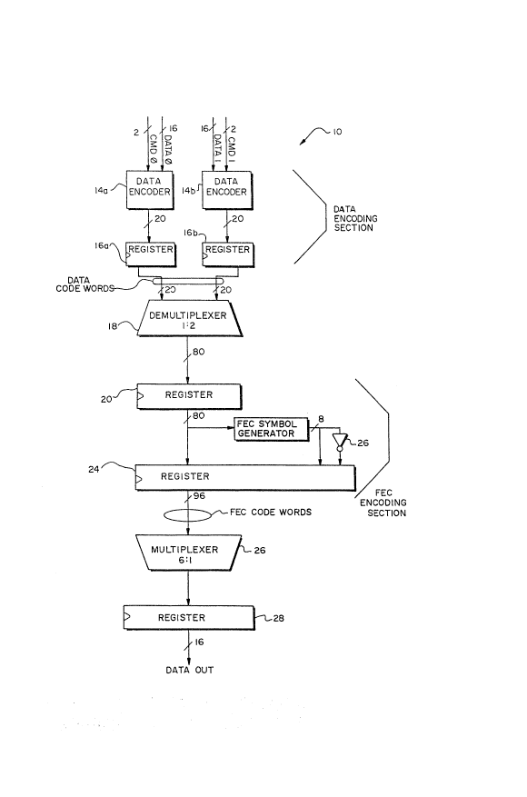
]FI~URE 1 shows a circuit for both data encoding and FEC
encoding of two 32-bit DATA signals into a 96-bit FEC code
block. The DATA signals each contain two 16-bit segments
DATA0, DATAl, each segment representing, e.g., data or command
information and being associated with one of two 2-bit CMD
signals CMD0, CMDl. Each CMD signal has a value which
identifies whether the associated segment contains command
information, i.e., is a command signal, or contains data
information, i.e., is a data signal.
Each segment DATA0, DATAl along with its associated CMD
signal is applied to a 16b/20b data encoder 14a, 14b. The data
encoders 14a, 14b translate the segments DATA0, DATA1 into
respective 20-bit data codewords, which are then stored in a
respective register 16a, 16b. The two 20-bit data codewords
stored in registers 16a, 16b are then provided to a 1:2
demultiplexer 18, which concatenates them with two other 20-bit
data codewords previously or subsequently generated by the data
encoders 14a, 14b.
The four 20-bit data codewords then are applied as an 80-
bit block to a register 20. Preferably, each data codeword in
the 80-bit block is, itself, DC balancedO If the 80-bit block
contains data codewords that are not DC balanced, then, its
data codewords have offsetting unbalances to the extent
possible, so that the entire 80-bit block has a minimal
cumulati~e DC-offset or is DC balanced. The technique for
achieving this is described below.
The 80 bits of data codewords are then applied to both an
FEC symbols generator 22 and a register 24. The FEC symbols
generator 22 generates an 8-bit FEC symbol, i.e., an ECC symbol
used for forward error control, from the data codewords. These
FEC bits are applied both to an 8-bit inverter 26 and directly
to the register 24. The inverter 26 inverts the bit values of
the FEC symbol, thereby generating inverted or complementary
FEC bits, which are supplied to the register 24.
The register 24 concatenates the data codewords, the FEC
bits and the inverted FEC bits in an interleaved fashion.
Specii--ically, each of the eight 20-bit data codewords is
followed by one of the 8 FEC bits and its complementary bi~.
In other words, complement FEC pairs are dispersed within the
FEC code block of encoded data. Not only does this effectively
limit the inter-codeword run lengths, but also the complement
FEC pairs are DC balanced and therefore leave unchanged the
cumulative DC-offs~t of the 80-bit block.
The 96-bit FEC code block is applied to a 6:1
multiplexer 26 to produce a 16-bit DATA-OUTPUT that is then
stored in register 28, ready for 16-bit serial transmission.
While the encoding circuit 10 processes 16-bit DATA inputs
using two parallel 16b/20b data encoders 14a, 14b, four
parallel 8b/lOb encoders can be used instead by suitably
adapting the circuit 10 as will be apparent to those in the
art. Various embodiments for 16b/20b and 8b/lOb encoding are
described in detail below.
A preferred embqdiment of each data encoder 14a, 14b uses
precoding and 8b/9b and lOb/llb subencoding. This results in
9-bit and ll-bit data codewords. The 9b/llb partitioning of
the 20B sub-block struct~re facilitates encoding and decoding,
and permits the constraining of both maximum run length and the
cumulative DC-offset. By appropriate selection of data
codewords, the DC unbalance in each 9-bit and each ll-bit
segment is constrained to one LOGIC ONE or LOGIC ZERO value,
which i8 the minimum unbalance possible with odd-length
segments. With 9-bit and ll-bit segments having opposite
unbalances, the composite 20-bit sequence can be made to be
balanced. Furthermore, use of the subset of 9-bit and ll-bit
data codewords that conforms to a 3~4/3 maximum run length
criteria, as explained below, limits the maximum run length
.
-14-
to 4.
With this type of data encoding, it is preferred that, in
generatinq the FEC code blocks, single FEC and FEC inverted
bits are placed in pairs between 9-bit and ll-bit segments to
reduce maximum run length.
The FEC code block thus contains a total of 16 F~C bits
and 80 bits of encoded data in the form of 4 20-bit sub-block
sections. Each sub-block is DC~balanced. The modular balanced
16B/20B sub-block encoding eases chip design, and enables the
use of 8/5, 16/1~, 32/30 as well as 64/62 data/command bit
length words.
In other words, the code block is composed of 4
structurally similar sub-blocks of 24 bits each. Each 24-bit
sub-block contains 20 bits of encoded data, which is further
sub-divided into 9-bit and ll-bit segments. In between each
segment is one bit of the FEC an~ its inverse. At the end of
the ll-bit segment is an additional FEC and inverted FEC bit.
Since each 24-bit sub-block contains 2 FEC bits and there are 4
sub-blocks, the entire block contains 8 FEC bits. The block
structure is therefore as follows:
BLOCK =
[24 bit SUB-BLOCK] ~24 BIT SUB-BLOCK] +
[24 bit SUB-BLOCK] [24 BIT SUB-BLOCK]
SUB-BLOCK =
[9 BITS ENCODED DATA] [FEC BIT] [INVERSE FEC BIT] +
[11 BITS ENCODED DATA] [FEC BIT] [INVERSE FEC BIT]
(The "+~ symbol in the preceding diagram represents
concatenation, i.e., that the data represented on two
.
, ~ ~ , .! . , : '
-15-
consecutive lines of the page are actually one continuous bi
stream.)
The FEC symbols generator 22 preferably uses a Hamming
distance 4 Hsiao block encoding procedure that corrects single
errors and detects double errors. To be compatible with
available multiplexers and demultiplexers and other commonly-
used interfaces, the code length is a multiple of 8. With 8
bits of forward error control symbols, it is possible to
protect blocks (including FEC bits) containing from 64 to 127
bits. The data codeword length of ~0 bits (i.e. 4 encoded 20-
bit words or 8 10-bit words) is advantageous since it reduces
FEC overhead and increases link efficiency.
Thus, the invention provides forward error correction
capability and good signal properties (i.e., short maximum run
lengths and minimal cumulative DC unbalance or periodic
balance) for use, e.g., with fiber optic transmission media.
The 25~ overhead attributable to the data encoder section and
the 25% overhead attributable to the FEC encoding section are
accomplished using a block encoding procedure that is both
simple and practical in implementation.
b. Introduction to Run Lenqth.
The maximum signal run length of the bit stream can be
fixed by the maximum run length properties of the individual
encoded words comprising the bit stream. The run length
properties of encoded words can be analyzed in terms of the
beginning run length, a middle maximum run length, and an end
run length. A code that iæ constrained to have a run length of
no more than i at the beginning, a run length of no more than j
in the middle, and a run length of no more than k at the end,
can be termed a i/j/k maximum run length encoding, where "i,"
"j" and "k" are integers. For example, contiguous sequences of
2/5/3 codes will generate a serial stream that has a maximum
.' : ' ' ~ ~ ' ' -
'.
-16-
run length of i + k = j = 2 + 3 = 5. Likewise, a continuous
sequence of 3/4~3 codewords will generate a serial stream that
has a maximum run length of i + k = 6, since "j" is less than i
+ k for the 3/4/3 codewords. However, a sequence of 3/4/3
codewords that are separated by a series of bits selected to
have a beginning and ending run length of "c" ("c" being a
positive integer) will yield a maximum run length for the bit
stream of the greater of "c + i", ";" or "k + c," which
for 3/4/3 codewor~s is c + i = k + c. Where 3/4/3 codewords
are separated by a complementary pair of bits (e.g., "1"/"0" or
"O"/"l" FEC bits), c = 1 and the maximum run length of the
resulting bit stream is 1 + i = k + 1 = 4.
The number of codes that conform to given
beginning/middle/end run length criteria can be counted by
listing all codewords of the required number of bits and
deleting codewords that violate the run length criteria. Such
a procedure can be carried out rapidly by a computer processor.
For future reference, the table of FIGURE 2 is a computer-
generated list of the number of codes that conform to various
run length criteria.
c. 8b/lOb Data Encodinq With FEC ComPlementary Pair
SeParators.
As mentioned above, data encoding can be performed
advantageously using 8b/lOb encoding. In accordance with the
invention, a novel, direct 8b/lOb encoding approach, using
complement FEC bit pairs to restrict run lengths at each end of
lOb codewords, enables 2a data codes and 27 command codes to be
generated. This code has a maximum run length of 4, a maximum
cumulative DC-offset of 4 one or zero bits within a codeword,
and a maximum cumulative DC-offset at the end of each codeword
of a single bit.
-17-
With this 8b/lOb code, it is not possible consistently to
have periodic code ~alance (i.e. balance at the end of each
codeword); there are only 228 balanced 10-bit codewords that
satisfy the 3/4/3 run length criterion, not enough to allocate
a separate 10-bit balanced codeword to each of the 256 possible
8-bit uncoded data words. The best that can be achieved is to
limit the cumulative DC-offset at the end of each codeword to a
single "1" or "O" bit. According to the present invention,
this is accomplished by mapping as many as possible (up to 228)
of the 8-bit data words onto balanced 10-bit codewords, and
mapping each of the remaining 8~bit data words onto one of two
alternative 10-bit codewords that are bit-wise complements of
each other and have an unbalance of only one bit. Whenever an
~-bit data word is to be encoded which maps onto one of the
unbalanced 10-bit codewords, the encoder selects that one of
the two alternative codewords for that data word that tends to
restore cumulative balance.
In other words, if the cumulative unbalance contains an
excess of "l"s, the next unbalanced codeword is selected to
have an unbalance of the opposite sign, i.e., an excess
of "O"s. This is achieved by selecting, as the second
unbalanced codeword, one whose unbalance is opposite to that of
the first. By so selecting the unbalanced codewords to offset
the unbalance of the most-recent prior unbalanced codeword, the
net cumulative DC-offset at the end of any block of codewords
(and hence at the end of a complete message) will not be
greater than a single "1" or "O" bit. Therefore, although the
bit stream is not assured of being periodically balanced, the
cumulative DC-offset is con trained to be within well defined
limits.
The number of available codewords meeting the aforesaid
run length and cumulative DC-offset criteria can be calculated.
The total number of balanced 10-bit words is the combination of
--18--
10 items taken 5 at a time, or 10!/(5!*5!) = 252. Therefore,
it is impossible to represent 28 = 256 data values with
balanced 10-bit codewords. Moreover, as shown in the table of
FIGURE 2, there are only 228 balanced 3/4/3 codes; 3/4/3 codes
are preferred because they can be used with complementary FEC
bit pairs to create maximum run length 4 bit streams. However,
as also shown in FIGURE 2, there are additional codewords that
have an unbalance of a single "1" bit (i.e., six "l"s and four
"O"s), 165 of which meet the 3/4/3 criteria. Likewise, there
are an equal number of codes that have an excess "O" bit.
Therefore, 228 input values can be represented with balanced
codewords, and an additional number (up to 165) of input values
can be represented by either of two minimally unbalanced 10-bit
codewords, each one of the codewords being the bit-wise
complement of the other. With this approach, there are a total
of 228 + 165 = 393 3/4/3 codes available for use. Of these 393
10-bit codewords, 256 are needed to encode the 8-bit data
words, so the remaining 137 10-bit codewords are available to
encode up to 137 different command words (i.e., more than
enough to encode the 128 possible 7-bit command words). Thus,
with this encoding scheme a 10-bit codeword can represent an 8-
bit data word or a 7-bit command word. The use of 3/4/3 codes
separated by complementary FEC bit pairs guarantees a maximum
run length of 4.
d. Illustrative Embodiment of a Sinqle, Direct 8b/lOb
Data Encoder.
FIGURE 3A depicts a single, direct 8b/lOb data encoder 40.
The encoder 40 includes an unbalance detector 42, a toggle flip
flop circuit 44 and a memory 46. The encoder 40 distinguishes
between 8--bit input words whose corresponding 10-bit codewords
are balanced from those whose codes are unbalanced. For those
latter input values that have been mapped onto complementary
?~
--19--
pairs of unbalanced codewords, it selects an unbalanced
codeword that takes the prior run stream history into account
and produces a code stream exhibiting the minimum unbalance.
Thus, whenever a codeword has more LOGIC ONE's than LOGIC
ZERO's, the next unbalanced codeword selected by the encoder 40
will be of the opposite unbalance, i.e., more LOGIC ZERO's than
LOGIC ONE's.
The unbalance detector 42 tests whether the code will be
balanced or not; that is, it recognizes whether a codeword is
unbalanced. When a codeword is unbalanced, the unbalance
detector 42 generates an UNBALANCE signal whose value is LOGIC
ONE. When the codeword is balanced, the UNBALANCE signal value
is LOGIC ZERO.
The unbalance detector 42 has an ~ND gate 50 to which the
three most significant bits (MSB's) of the input signal are fed
as separate inputs A5-A7. (~he least significant bits (LSB's),
designated AO-A6 are not used in the unbalance detector 42 for
reasons described below.) The output of the AND gate 50 is
applied as a first input to an OR gate 52, with the other input
being a CMD signal indicative of whether the input signal
contains command information. The output of the OR gate 52 is
the UNBAL~NCE signal.
The operation of the unbalance detector 42 can be
understood with reference to the corresponding truth table
given in FIGURE 3B. To understand the table, however, consider
the following: It can be seen from FIGURE 2 that there are 228
lOb balanced codewords (i.e., lOb codewords having 5 LOGIC
ONE's) that also have 3/4~3 maximum run lengths, and 165 lOb
codewords having unbalances of 1 (i.e., codewords having 4 or 6
LOGIC ONE's) and 3/4/3 maximum run lengths. Converting these
numbers of codewords to binary yields:
228 (dec~ - 11100100 ~bin)
,
.
.:
! " . . ', ., . u . ` ~
-20
165 (dec) = 10100101 (bin)
These numbers can be rounded down, resulting in 224 (dec) =
11100000 (bin) balanced codewords and 160 (dec) = 101000~0
(bin) unbalanced codewords available which meet the
stated 3/4/3 maximum run length criteria. Thus, input data
signal values less than 224 (111000002) can be represented by
balanced codewords, input data values from 224 to 255 can be
represented by unbalanced codewords, and input commands
from 256 to 383 (a total of 128) can be represented by
unbalanced codewords. With this scheme, the criterion for
recognizing an unbalanced codeword is that the three most-
significant bits (A5, A6, A7) are l's.
Now, with that background information having been given,
the table of FIGURE 3A can be readily understood. In the
table, "1" indicates a LOGIC ONE, a "0" indicates a LOGIC ZERO,
and an "x" indicates either a LOGIC ONE or LOGIC ZERO. By
using only the three most significant bits of the data input
signal and the command signal, the unbalance detector circuit
42 is simplified.
As can be seen, the output of the AND gate 50 is a LOGIC
ZERO when its three input lines A7-A5 are no~- all "1," which
indicates input signal values below 224 and corrasponds to
balanced codewords. The output of the AND gate 50 is a LOGIC
ONE whenever its input lines all assert "1," which indicates
input si~nal values equal to or above 224 and corresponds to
unbalanced codewords. The OR gate 52 generates an UNBALANCE
signal having a value of LOGIC ONE whenever the output of the
AND gate 50 is a LOGIC ONE or whenever the CMD signal is
asserted, i.e., has a LOGIC ONE value, which, in either case,
indicates an unbalanced codeword. on th~ other hand, the OR
gate 52 generates an UNBALANCE signal having a value of LOGIC
ZERO whenever any of the input signal bits are LOGIC ZERO,
r~
which indicates input signal values less than 22~, and the CMD
signal is not asserted. This condition corresponds to balanced
codewords.
The toggle flip flop circuit 44 serves to preserve the
present state of the UNBALANCE signal until the next unbalanced
code is generated, using an exclusive OR gate 44a and a memory
device such as a D-type flip flop or register 44b to store the
last UNBALANCE signal. Each time the next codeword to be
transmitted is unbalanced, the flip flop reverses its state.
The output of the toggle flip flop circuit 44 is applied to the
memory 46 for selecting the appropriate code balance for the
next unbalanced code.
The memory 46 preferably is implemented as a read-only
memory ("ROM") or programmed logic array ("PLA"), and performs
a lOb/lOb encoding by using a stored lookup table of codewords.
The lookup table provides a 10-bit codeword for each 10-bit
input. The 10-bit input consists of the single-bit UNBALANCE
output of the toggle flip flop circuit 44, as well as the
command signal CMD and data bits A7-AO, which are applied to
the memory 46 after being delayed (in a delay device 47, such
as a register bank) to arrive in the same clock cycle as the
corresponding output of circuit 44. The memory 46 implements
the codeword-assignment scheme outlined above, and, for those
data inputs represented by two complementary unbalanced
codewords, it chooses between the two codewords in accordance
with the UNBALANCE output of the toggle flip flop circuit 46 so
as to offset a previous unbalance of a prior encoded input.
The codeword assignments needed to accomplish this use the
output from the toggle flip flop circuit 44 to determine what
the unbalance of the codeword should be, on the basis of the
last input's unbalance.
FIGURE 3C depicts an alternate type of encoder. The
encoder RON 46c can in general be the same as ROM 46 of
. ... .
. . : . . : ,: . ~ : , .
. :- ,. ::: :
" ~". ` ; . ` '` ! ~-
--22--
FIGURE 3B, with the exception that each location additionally
inclucles an eleventh bit, i.e., the UNBALANCE signal, to
indicate whether the other ten bits constitute a balanced
codeword. This bit is fed to a toggle flip flop circuit 47
identical to the circuit 44 of FIGURE 3A to produce a similar
input to the decoder ROM 46c.
FIGURE 3D illustrates the lookup table stored in encoder
ROM 46c. The first three columns in the table represent inputs
to the ROM 46c (i.e., ROM addresses), the fourth column
represents the outputted 11th bit or UNBAL~NCE signal, and the
fifth column represents the 10-bit codeword output.
The lookup table supplies the UNBALANCE signal to a toggle
flip flop circuit 44a, which then applies it to the memory 46a,
as described in conjunction with FIGURE 3A.
e. Multiple Octet-Based Data Encodinq Circuit.
FIGURE 4 shows a composite encoder 60 for concurrent block
encoding of multiple (e.g., four) octet-based words in
parallel. The circuit 60 includes four parallel unbalance
detectors 62a-62d, four 10b/lOb component encoders 66a-66d,
each generally as shown in FIGURE 3A, and a memory 74.
Attaining the minimal unbalance when four octet-based
words are to be processed concurrently presents a complication
not encountered in non-block encoding. Specifically, each 10-
bit input word to each component encoder 66a-66d in the
composite encoder 60, containing either data or command
information, will indicate whether the output codeword is to be
unbalanced, as described above in conjunction with FIGURE 3A,
but the proper choice to minimize unbalance in the block
depends on the performance of all the component encoders, and
thus the component encoders are inter-dependent and must rely
on externally supplied information (external to each component
encoder's own circuit) to minimize the unbalance of the
,:
.. . .
' ,: '. '', ~ ' - ' ' - '
- , . ' .
-23-
resu].ting run stream.
One way of providing that external information is to
supply a feed forward signal in series from one component
encodér to another, and from the last component encoder back to
the first, to influence the selection of succeeding codewords
to obtain a minimal cumulative DC-offset. Unfortunately, this
approach can not be used in some applications because the time
required for the feed forward signal to ripple from encoder to
encoder generally will be too long to be accomplished in a
single clock cycle.
A faster and hence preferred approach is shown in FIGURE 4
as entailing the use of a select-unbalance-signal generator
comprising four unbalance detectors 62a-62d, a read-only
memory 74, and a latch 76. The detectors 62a-62d feed their
respective UNBALANCE signals U1-U4 as address signals to the
memory 74, which also receives a PRIOR BALANCE signal a~ part
of its address input. The memory 74 may be a single 5-
inputs/5-outputs ROM or PLA. The memory 74 stores a SELECT
UNBALANCE lookup table. The output of this lookup table is -
provided as a SELECT UNBAhANCE signal over four signal lines
Sl-S4 to the composite encoders 66a-66d. The SELECT UNBALANCE
signal indicates the appropriate DC unbalance state of the
codeword to be selected by each of the four composite
encoders 66a-66d. one NEXT BALANCE output bit of the memory 74
is provided to the latch 76 whose output is a PRIOR BALANCE
signal, which indicates the unbalance to be used to generate
the next SELECT UNBALANCE signal. The latch 76 holds the NEXT
BALANCE signal and then supplies it to the memory 74 in the
clock cycle in which the next set of four UNBALANCE signals Ul-
U4 is supplied from the unbalance detectors 42a-42d. Thus, the
NEXT BALANCE signal is a feedback signal which is
recirculated to provide a history of the prior unbalance.
Latches 78 on the circuit input lines act as buffers to
'"
:........... ' ' ' ' ' ` ' ,, ~'
, :.
o ~ c~
-24-
receive the CMD and A7-AO inputs and provide them in the same
clock cycle both to the unbalance detectors 62a-62d and to the
encoders 66a-66d. The latches 76, 78 preferably are clocked at
the same time.
The SELECT UNBALANCE table ~tored in memory 74 is shown in
FIGURE 4A, wherein a PRIOR BALANCE of "O" indicates that the
prior cumulative DC~offset is -1 (i.e., six "0"s and
four "l"s), and a PRIOR BALANCE of l'1" indicates that the prior
cumulative DC-offset is +1 (i.e., six "l"s and four "0"s).
Similarly a NEXT BALANCE of "1" indicates that the next
cumulative DC offset of +1 (i.e., six "l"s and four "0"s), and
a NEXT BALANCE of "0" indicates that the next unbalanced
codeword should have a cumulative DC-offset of -1 (i.e.,
six "0"s and four "l"s).
In response to its input signals that indicate which
codewords will be unbalanced, the BALANCE-TO-SELECT table
selects the unbalance state to be used by the encoders 66a-66d.
A "O" in one of the input columns (Ul-U4) of the SELECT
UNBALANCE table indicates that the selected codeword will be
balanced, and a "1" indicates that it will be unbalanced. The
SELECT UNBALANCE table outputs, i.e., the SELECT UNBALANCE
signals, are "0" if the selected codeword is to have more "0"s
than "l"s, and "1" if the selected codeword is to have
more "l"s than "0"s. The SELECT UNBALANCE table shows SELECT
UNBALANCE signal values of "X" (either "1" or "0") for balanced
inputs because, in that case, the encoders 16a-16b preferably
will output a codeword independent of the unbalance select
lines.
Whenever the PRIOR BALANCE signal bas a value of "1", all
output bits S1-S4 from the lookup table are the binary
complements of their values when the PRIOR BALANCE signal has a
"0" value. As depicted in FIGURE 4A, the size of the SELECT
UNBALANCE table îs halved in order to save space on the page,
- ' : ~ . : ' ~ '
both values for the complementary entries being shown as
separated by a slash. The left value is used for PRIOR
BALANCE = "0" and the right value for PRIOR BALANCE = "1." (An
alternative way to implement this is to use a bank of par~llPl
exclusive OR gates at the output of memory 74, with each of the
output signals Sl-S4 of the lookup table being provided as a
first input to a different one of the exclusive OR gates, and
the PRIOR BALANCE signal from the latch 76 being applied as a
common second input to each of the exclusive OR gates.)
f. 16b/20b ~ncodinq Usinq 8b/~b and 10b/llb Sub-Encodin~. -
An 8b/lOb code necessitates the use of some unbalanced
codewords. By doubling the codeword size to 20 bits, however,
a code in which all codewords are balanced can be obtained,
even though the siæe of the input word is also doubled, to 16
bits.
To accomplish this, 10 bits of the 20-bit block must have
the same logic value. Therefore, there are
C(20/10) = 20!/10!*10! = 184,756 distinct balanced codewords
having 20-bit lengths. Therefore, well over 2~5 = 65536 input
values can be represented by the available repertoire of
balanced 20-bit codewords. (On the other hand, a 16b/19b code
results in some unbalanced codewords, and a 16b/18b code
results in too few codewords of any type.) A 16b/20b data
encoding procedure also offers the advantaqe that it, like
the 8b/lOb code, uses input values that are a multiple of
eight, and therefore are compatible with octet-based hardware
and programs.
In order to perform 16b/20b encoding using ROM or PLA on
CMOS chips using current technology, the 16b/20b encoding
procedure preferably is divided into two or more sub-encoding
procedures of approximately equal size to minimize the chip
area.
s~
-26-
Dividing the 16b/20b encoding into two 8b/lOb encodings
results in only C(10/5) = 252 balanced codewords, i.e. not
enough to represent the desired 28 = 256 input values for each
8-bit input value. If unbalanced 10-bit codewords are used to
augment the available repertoire, on the other hand, enough
codewords can be obtained, but, of course, then a DC unbalance
is being introduced.
However, if the 16b/20b encoding is divided into two
unequal parts -- ~b/9b and a lOb/llb sub-encodings -- then
there are enough available balanced 20-bit composite codewords.
While neither the 9-bit nor the ll-bit codeword can be balanced
-- odd-length codewords cannot be balanced -- the 9-bit and ll-
bit codewords can be constrained both to be minimally
unbalanced and to have the opposite unbalance so that, when the
codewords are concatenated, the resulting block is balanced.
In a 9-bit code, there are a total of C(9/4) = 126
codewords with an excess "l" bit and 126 with an excess "O"
bit. The 252 such codewords will be used separately; i.e., a
9-bit codeword and its complement will be used in this scheme
to represent different input values; they will not be used as
alternative ways of representing the same input value. In an
11-bit code, there are a total of C(11/5) = 462 codewords with
a single excess "1" bit and the same number of codewords with a
single excess "O" bit. However, unlike the 9-bit codewords,
the complementary ll-bit codewords must be used as an alternate
representation of the same input; when one of the available 252
9b codewords is used, the 11-bit codeword's unbalance must
complement the 9-bit codeword' 8 unbalance to yield overall
balance for the complete 20-bit block. There are therefore
252*462 = 116,424 codewords, more than enough to represent 2
values.
Unfortunately, the use of all 116,424 codewords provides a
very loose limit on the maximum run length of the encoded bit
:
- . :
-27-
stream. For example, the use of 000011111 and 11111000000,
when concatenated to form the 20-bit blocks, would result in a
maximum run length of 10. However, the use of forward error
correcting code bits permits the maximum run length to be
limited -- using 96-bit blocks each protected by 8 FEC bits and
8 complement FEC bits, with complementary FEC bit pairs placed
between each of the four 9b and llb sub-segn)ents. In that
case, the maximum run length using the above words would be 7.
As can be seen from the table of FIGURE 2, there are a
total of 391 11-bit codewords and 113 9-bit codewords with a
single excess "0" bit that conform to the 3/4/3 maximum run
length criteria. There are also 113 such 9-bit codewords with
a single excess "1" bit. If this restricted set of codewords
is used with complementary FEC pairs between each 9-bit and 11-
bit codewords, then a maximum run length of 4 can be achieved.
There are 391*2*113 = 88366 such 4-bit run length, balanced,
20-bit codewords representing data, more than enough to
represent 216 = 65536 input values, so 22830 codewords are
available for other uses.
Of these 22830 additional codewords, one can, for example,
use 214 = 16,384 for codewords representing command
information, i.e., "command codewords." Preferably, command
codewords are identified as such by the setting of a "command"
line which is an input or output line that is separate from the
16 data input or output lines. In other words, the setting of
the command line identifies the codeword as representing
command information, while ~he other 16 lines specify the
particular command. However, because the codeword repertoire
does not allow 2l6 command values, the two most significant
bits are not available when the command line is active. In
that case, 214 = 16,384 values remain for representing command
codes. That nevertheless leaves 6446 (>4096 = 2l2) codewords
for representing an additional data type or category, which can
-28-
be c;alled "idle" codewords. It is desirable for the 16b/20b
codewords to be able to represent not only 2l6 data words and
214 command words, but also the third category of 2l2 idle
words.
The idle codewords can be used for a variety of purposes.
For instance, they can be sent across a link for initialization
purposes or sent if no data is available at the input of the
link to maintain the desired maximum run stream properties
(idle link). The availability of 212 12-bit codewords ~that
are used in this embodiment as idle words) also enhances the
capability of the 16b/20b code to represent octet-based data
and commands, as described below.
Although there are 88,366 balanced 20-bit data codewords
providing a maximum run length of 4, it is not straightforward
to implement such a code in 8b/9b and 10b/llb encoders without
exceeding the repertoire of available conforming codewords.
Specifically, if the encoder input lines are simply the lines
that carry the 16-bit input, there is no constraint on the
input values. Accordingly, the number (28 = 256) of possible
input words to an 8b/9b encoder would exceed the number (226)
of conforming 9-bit codewords, and the number (2~ = 1024) of
possible input words to a 10b/llb encoder would exceed the
number (391) of conforming pairs of ll-bit codewords. Logic
translation thus is required.
While this logic translation can be accomplished by
'Irandom logic" of AND or OR gates, a preferred implementation
is a ROM or PLA lookup table. The ROM or ~LA that performs the
necessary translation in the data encoding process is called
"pre-encoder" logic or, simply, a "precoder."
The precoder preferably generates a number of precoder
codewords which, when applied as inputs to the 8b/9b and
10b/llb encoders, does not exceed the code repertoire limits of
the 8b/9b and 10b/llb encoders, and yet permits the use of a
-29-
high fraction of the encoders' repertoires. Also, the number
of data lines that pass through the precoder preferably is a
small fraction of the total 16 input data lines. Otherwise,
when augmented by a command line and an idle line, the total
number of lines would make the precoder ROM or PLA chip area
too large. Conversely, minimizing the number of da a lines
translated by the precoder causes a loss in the number of
values that can be sent to the 9b and llb encoders.
As indicated above there are 226 9-bit values and 391 11-
bit values that provide 20-bit balanced codes with a maximum
run length of 4. Expressing these values in binary yields:
226 (dec) = 11100010 (bin)
391 (dec) = 110030111 (bin).
It is apparent that if no values equal to or greater
than 11100000 = 112 are sent to the 8b/9b encoder, and no
values equal to or greater than llO000000 = 384 are sent to
the lOb/llb encoder, the inputs will not "overflow" the
capability of either encoder to provide codewords. In effect,
no input to the 8b/9b encoder should have all three most
significant bits set, and no input to the lOb/llb encoder
should have both of the two most significant bits set.
g. 16-Bit-Word-Oriented 16b/20b Encoder Using 8b/9b and
_Ob/llb Sub-~ncoders.
A composite 16-bit-word-oriented 16b/20b encoder 80 is
shown in FIGURE 5. The encoder 80 includes a precoder 82, an
8b/9b component encoder 84, and a lOb/llb component encoder 86.
For conceptual purposes, the drawing also depicts an inverter
88. The inputs of the encoder 80 consist of 16 bits of data
D15-DO (with D15 being the most significant bit), a command
i` ' '` ' ~` `!
-30-
line input CMD, and an idle line input IDLE. The data input
lines Dll-D5 bypass the precoder 82 and are coupled directly to
inputs A7-Al of the 10b/llb encoder 86. The data lines D4-Dl
also bypass the precoder 82 and are coupled to inputs B4-Bl of
the 8b/9b encoder 84. The input line D0 is connected to the Bo
input of the 8b/9b encoder 84 and determines the unbalance of
the encoder output. The inver er 88 is included to indicate
that the unbalance of this encoder's output is opposite that of
the 8b/9b encoder's output, although, of course, an inverter is
not necessary to achieve this result since the lookup table of
the 10b/llb encoder 86 can be arranged to accomplish this
result directly.
Encoder 84 provides an output with an excess of a
single "O" if the D0 line is not set, while encoder 86 provides
an output with an excess of a single "1." The output of both
encoders when the D0 line is set are the complements of their
outputs when it is not. The lookup tables of encoders 84, 86
respond to the signal on the D0 line to generate the required
codeword. Alternatively, complementary data, of course, can be
generated by using a linear array of exclusive OR circuits.
The 9-bit and ll-bit codewords stored in encoders 84
and 86, respectively, preferably are selected from a computer-
generated list of codewords having a cumulative DC-offset of 1
bit and a maximum run length of 3/4/3. As described earlier
under Section (b), antitled "Introduction to Run Length," this
list can be generated by programming a computer to sequence
through every possible 9-bit and ll-bit codeword and test each
word to discover which ones satisfy both the l-bit cumulative
DC-offset criterion and the 3/4/3 maximum run length criterion.
The 9-bit and ll-bit words which do satisfy both criteria are
stored as codeword values in encoder ROM's 84 and 86,
respectively.
The translation carried out by the precoder 82 is
. - : ~.
.
' ~ ~
.
.
,
- ;?
-31-
represented by the table of FIGURE 5A. As can be seen from the
right hand side of the table, A9 and A8 are never both "1"
simult:aneously, and not all three of B8, B7, B6 are "1"
simultaneously. Therefore, the use of input values to the
8b/9b and 10b/llb encoders that would exceed the repertoire of
conforming codes has been avoided. Note that the values
for D14 and D15 are given as X for commands and idles and, in
addition, that D12 and D13 are given as X for idles. The ROM
and PLA outputs are the same regardless of the values of these
lines in the indicated situations. Note also that, because of
the lines bypassing the precoder 82, a total of 215 data, 214
command, and 212 idle words can be encoded.
h. 16b/20b Encoder For Octet-Based Data.
In the above-described 16b/20~ encoding, the input to the
encoder 80 was a 16-bit word containing either data or command
information, but not both. 16b/2Qb encoding can also
accommodate octet-oriented input values; i.e., two 8-bit words.
Each 8-bit input word can represent either 8-bit data or 5-bit
command information. Thus, the 16-bit input value can be a
data-data sequence (i.e., each octet includes data), a command-
command sequence (i.e., each octet includes command
information!, a data-command sequence (i.e., the first oct~t
contains data while the second octet contains command
information) or a command-data sequence ~i.e., the first octet
contains command information while the second contains data).
In addition to the sixteen data lines, there are two
additional command lines that together indicate the contents of
the other sixteen, i.e., whether they are data-data, command-
data, etc. In data-data sequences all sixteen lines carry
data, so there are 2l6 possible input words, each of which must
be assigned a separate code.
The system provides for only thirty-two (=25) different
'. ' ' ` : '
-32-
possible commands; the three most significant bits of an octet
that ~ontains a command in a data-command sequence are expected
to be zeros, while all eight bits of the data octet are used.
For a data-command sequence, therefore, 25 X 28 = 213 different
possible input words must be assigned codewords, and another
213 must be assigned to command-data sequence~, for a total of
214 codewords for data-command and command-data sequences
together. Another 25 X 25 = 2' codewords are needed for the
allowed command-command sequences.
Rather than introduce additional logic to convert from two
octet input words to one 16-bit input word for processing in
the encoding circuit of FIGURE 5, there exists a simpler
approach, namely, provide a suitable precoder translation
lookup table to accomplish the desired task.
Shown in FIGURE 6 is a 16b/20b encoding circuit 90 using
this approach for encoding two octet-based input values. In
FIGURE 6, the two 8-bit inputs are represented by data lines
Al-A8 and B0-B7, respectively. A l-bit command/data line
A-CMD indicates whether the 8-bit input word Al-A8 represents a
command word or a data word. Another l-bit line B-CMD
indicates the same thing for input word B0-B7. A precoder 92
receives command signals A-CMD, B-CMD, and input values, e.g.,
data or command information, A8-A6, B7-B5. Outputs A9'-A6'
from the precoder 92 are applied to a lOb/llb encoder 94, which
also receives input values A5-Al. The 10b/llb encoder 94 is
identical to the encoder 86 of FIGURE 5. Other outputs B7'-B5'
of the precoder 92 are provided to an 8b/9b encoder 96, which
also receives signals B4-Bl and the BALANCE signal B0. The
8b/9b encoder 96 is identical to the encoder 84 of FIGURE 5.
The BALANCE signal BO is inverted by inverter 98 and is applied
as yet another input A0 to the encoder 94.
FIGURE 6A shows the truth table implemented by
precoder 92, where the first group of columns represent input
. - ~
.
,
.
- ' ' ': .
; J ,~
lines (e.g., ROM address lines), and the second group of
col~lms (denoted by "prime" superscripts) represents output
lines; (e.g., values stored in the ROM). In order to shorten
the printed representation of the truth table in FIGURE 6A, the
first 64 rows of the truth table are represented by a single
row in that drawing. In the table, "X" indicates a signal
whose value does not affect the output. The D's indicate the
corresponding entries can be either "O" or "1." Unlike X's,
though, D's on the input side indicate that different values of
those input signals result in different values of the output
signals represented by D's.
When CA = CB = O, both input words Al-A8 and BO-B7
represent data words rather than command words. In this case,
the precoder 92 performs a 1 to 1 mapping between the six
precoder data inputs (A8-A6, B7-B5) and the seven precoder data
outputs (B7'-B5', A9'-A6'~. Any one-to-one mapping may be
used, so long as the mapping does not violate the two
constraints necessary to prevent overflow of the 8b/9b encoder
and the lOb/llb encoder. The two constraints are that at
least one of the three lines B7'-BS' must assume the value
LOGIC ZERO, and at least one of the two lines, A8' and A9' must
assume the value L~GIC ZERO. In the table of FIGURE 6A, input
data for the two octets is expressed in terms of the lOb~llb
encoder inputs A9-AO and the 8b/9b encoder inputs B7-BO.
External data is applied to the eight Al-A8 and eight BO-B7
lines. BO-B4 inputs bypass the precoder to directly enter the
8b/9b encoder. BO determines the unbalance state of the 8b/9b
encoder output and is inverted and sent to the AO input of the
lOb/llb encoder to force balance of its output to be
complementary to that of the 8b/9b encoder output. The Al-A5
lines also bypass the precoder to directly enter the lOb/llb
-34-
encoder. Input lines A~-A8 and B5 B7 as well as the command
lines A-CMD and B-CMD enter the precoder (8 input lines) and
seven output lines A9'-A6', B7'-B5' exit the precoder.
i. Forward Error Correcti~n Encodin~.
The type of forward error correction code employed can be,
for instance, a single error correction, double error detection
code and, in particular, a Hamming distance 4 code such as
devised by Hsiao (cf. the book "Error Control Coding" authored
by Shu Lin ~ Daniel J. Costello, Jr., PRENTICE-HALL 1983, pages
498-502). Such codes are linear in that the sum of any two
encoded values results in another encoded value. They are also
systematic in that the encoded data portion is unchanged from
the unencoded data. Therefore, in essence, an FEC bits are
added to the data codewords such that the combination of FEC
bits and data codewords provides distance 4 encoding. The FEC
bits can be generated by multiplying a lxB matrix data word by
a BxP FEC matrix to form a lxP FEC symbol matrix, where "B"
represents the total number of bits of the data codewords in
the block and "P" represents the number of FEC bits. The total
number of bits in the block is L = B + P.
In the present case, an 80-bit block (i.e., 4 20-bit data
codewords) is being protected by 8 FEC bits. Hence, B = 80 and
P = 8. To generate the 80 rows of the FEC matrix, 8-bit vector
s~quences are used, which each contain an odd number of "1"
bits, this odd number being at least 3. Because there are
only 8!/3!5l = 56 vector sequences with 3 "l" bits and there
are 80 bits to protect, some number of the complement type of
8-bit vector sequences containing 5 "1" values must also be
used. Since there are also 56 complement sequences, leading to
a total of 112 (there are also an additional set of 8 vector
sequences containing 7 "1" values that need not be used) and
only ~0 bits are to be protected, ~he choice of which 80 of the
112 vectors to use is arbitrary. Minimizing the number of "1"
bits in the vectors can minimize the number of active gates
required for encoding and decoding.
A preferred method for generating FEC bits is to use
cyclically independent code sequences (i.e. sequences that can
not be inter-converted by rotating sequence elements). In
terms of sequences containing 3 "1" bits, the following 7
cyclically independent variations are readily enumerated:
[00000111], tOOOO1011], [00010011], tOO100011]
[01000011], [00010101], [00100101]
Rotating all of these sequences through all 8 of the possible
cyclical variations produces a total of 56 FEC codes. Also,
the complement sequences containing 5 "l"s can be generated by
inverting all bits of the codes obtained for the case
of 3 "l"s.
i. Illustrative Communication System.
FIGURE 7 shows a communication system 100 in accordance
with the invention. System 100 is a point-to-point fiber optic
data linX. The illustrated components of system 100 are
susceptible of implementation using, for example, two CMOS
chips that perform data coding, decoding and framing.
System 100 includes a transmitter section lOOa and a
receiver section lOOb. In the transmitter section lOOa, input
data is accepted by an encoder 102 as a 32 bit parallel stream,
where it is coded and forward error correction bits are added
so as to form an ECC codeword in a manner such as described
~}
--36--
above. Encoder 102 preferably is implemented as shown in
FIGURE 1. In the encoder 102, the data is also multiplexed up
to a 16-bit parallel word, and then passed to a 16:1
mult:iplexer ("MUX") 104, followed by a laser transmitter 106.
The serialized data is the input of a laser transmitter 106,
which drives link or channel 108.
In the receiver section lOOb, the optic signal received
over the link 108 is converted back into an electrical signal
and amplified by the optical receiver/transducer 110 and then
passed to a clock recovery module 112. The clock and retimed
data are recovered by the module 112 and applied to a
conventional 1:16 demultiplexer 114. The demultiplexer 114
provides 16-bit sequences of the electrical signal to a framing
and data recovery circuit 120. The framing and data recovery
circuit 120 performs further demultiplexing, framing to
determine the boundaries of the 96-bit FEC code blocks, and
error correction and data decoding to obtain a recovered data
stream. The recovered data stream is in the form of a 32-bit
parallel stream, including 32 bits of DATA and 2 bits of CMD,
similar to the form of the above-mentioned source data fed to
the transmitter section lOOa.
During encoding and decoding, control and status
information is accessed by respective micro-processors 122,124
through registers in the encoder 102 and decoder 120.
k~ Framinq of the FEC Code Block and Data Decodinq.
When the receiver 1OOb initially receives communication
signals, the incoming bit stream lacks any boundaries that
would identify the beginning and end of the FEC code blocks.
Consequently, the framing and decoding circuit 120 must
identify those boundaries, i.e., frame the FEC code block, in
'
order to be able to perform error correction and data decoding.
This typically takes place during initialization of the
receiver lOOb, prior to receipt of actual data.
FIGURE 8 depicts the framing and decoding circuit 120.
The 16-bit sequences from the 1:16 demultiplexer 114 are
applied, one at a time, to register 200. Register 200 then
suppl ies its contents, the 16-bit sequence, to a 1:6
demultiplexer 202 which generates a 96-bit output. This 96-bit
sequence is supplied to a register 204. The register 204
provides its 96-bit contents to framing circuitry 205, which
includes a syndrome generator 206, an FEC check 208, and an
error counter 210. The framing circuitry 205 treats each 96-
bit sequence as though it were an FEC code block and calculates
the number of errors contained in that block as indicated by
the bits of that sequence occupying the bit positions of the
FEC symbol.
Specifically, the 80 bits of the 96-bit sequence that
would contain data codewords and the 8 bits that would be FEC
bits if the sequence were properly framed are applied to the
syndrome generator 206. The syndrome generator 206 detects
errors in these 88 bits, and generates an 8-bit ERROR signal,
which contains all "O"s if there is no detected error, contains
an odd number of "l"s if the syndrome generator 206 detects a
~ingle-bit error, and contains an even number of "l"s if the
syndrome generator 206 detects a double-bit error. Such
syndrome generators are readily available as commercial parts
in a single integrated circuit chip.
At the same time as the syndrome generator 206 receives an
88-bit block of the 96-bit sequence, the register 204 supplies
the 16 bits from that same 96-bit sequence corresponding to the
8 FEC bits and their 8-bit complements to the FEC check 208.
-38-
The FEC check 20a compares the received bits and checks whether
each FEC bit is juxtaposed with its complement. If any
complementary pairs are not present, the FEC check 208 asserts
FEC-ERROR.
The error counting circuit 210 receives the 8 bit ERROR
signal from the syndrome generator 206 and the FEC-ERROR signal
from the FEC check 208. For each error indicated by the
syndrome generator 206, i.e., for each single-bit or double-bit
error, the error counting circuit 210 increments a counter.
If, for any 96-bit block, neither the syndrome generator 206
nor the FEC check 208 detects an error, the counter is reset to
zero.
If the counter reaches a pre-selected threshold, e.g., 8
errors, then the error counting circuit 210 supplies a signal,
BIT SLIP, to the SLIP or SKIP input of 1:16 demultiplexer 114.
This signal causes the demultiplexer 114 to skip one bit of the
incoming serial data stream, as mentioned above, so as to
change by one bit the alignment of the frame of the 96-bit
sequence provided to register 204. ~Demultiplexers having this
"slip" or "skip" function are readily commercially available.)
This new 96-bit sequence is then examined ~gain by the framing
circuitry 205.
This process continues until a predetermined nu~ber of 96-
bit sequences (e.g., 10) are found to be error free. At that
time, the receiver 100b is properly initialized and error
correction and data decoding can ensue.
Conventional Hsiao error correction circuitry 212 corrects
any detected errors in the data codewords of the now-framed 96-
bit FEC code block, and provides the data codewords to a
re~ister 218, which then provides them to a 2:1
multiplexer 220. The 2-1 multiplexer 220 provides a first pair
, . - '
.
`~ . ' t~
s ~ .J
-39-
of the data codewords, i.e., the first 40 bits, to a data
decoder 222. The data decoder 222 decodes the data codewords
it received to recover the data and command information
contained therein. The output of the data decodPr 222 is
stored in register 224 as 32-bit DATA-OUT and a 2-bit CMD-OUT
values. Then the 2:1 multiplexer 220 provides the remaining
two data codewords, i.e., the last ~0 bits, to the decoder 222
which again generates therefrom a 32-bit DATA-OUT signal and a
2-bit CMD-OUT signal.
An illustrative embodiment of the decoder 222 will now be
described. This decoder decodes data codewords formed, for
example, by the encoder. The data decoder 222 has two
identical, parallel decoding branches, each for decoding one of
the codewords. Within each branch, the 20 bits of the received
data codeword are sent to llb/lOb and 9b/8b decoders. Then,
the three most significant bits from the 9b/8b decoder and the
two most significant bits from the llb/lOb decoder are sent to
a post-decoder that performs an operation inverse to that of
the precoder 42 of FIGURE 5; that is, the lookup in the table
of FIGURE 5A (which is contained in the pre-decoder as well as
in the precoder 42) proceeds from right to left as shown in the
drawing. The output of the decoding circuit is then a total of
18 lines that reproduce the input of the encoding circuit 40 of
FIGURE 5.
There is, however, at least one difference between the
decoding circuit and the encoding circuit 40 -- there are no
valid words in the output of the decoding circuit that
correspond to both command and idle lines set. In the output
of the decoding circuit, the presence of "l"s on both command
and idle lines preferably is used to indicat~ the reception of
an invalid code.
-40-
IJsing the system 100, the properties sf the coded serial
data s.tream are optimized for transmission over the fiber optic
link ;L08. In accordance with various aspects of the invention,
the maximum run length is kept short to aid in clock recovery
and to minimize the low frequency energy, and the DC balance
allows reliable code retrieval with the use of a high-gain AC-
coupled receiver. Preferably, the maximum run length is four,
i.e., no more than four successive LOGIC ONE's or LOGIC ZERO's
may appear in the serial data stream when error free. The
cumulative DC-offset preferably is limited to plus or minus
four within each codeword, and to zero at the end of each 24-
bit sub-block. For these values, the overall efficiency of the
link 10~ of system 100 is 2/3.
1. Other Data Encodinq Techniques.
Hereinabove, the described encoding techniques all use
double encoding, i.e., first data encoding, preferably using
a 3/4/3 csde, and then FEC encoding of blocks (e.g., 96-bit
blocks) containing a plurality (e.g., four) of data codewords.
By dispersing the FEC bits between the data codewords, a
maximum run length of 4 is achieved for the resulting bit
stream of the communication signal.
Many of the novel techniques of error protection encoding
can be used advantageously with data encoding approaches other
than those described in conjunction with the illustrative
embodiments of the invention. For example, dispersal of
complementary bits or the use of 96-bit FEC blocks can be used
with the above-mentioned IBM 8b/lOb code. Furthermore, the
error protection encoding techniques described herein can be
used even where data encoding is not employed, i.e., where only
protection encoding of an unencoded bit sequence is desired.
:, : ' . ' ., - :
. , ' . ' ~ ~ :
- ' - ~ ' ~ '
.
..
-41-
On the other hand, applications in which only data
encoding is desired also can obtain many of the advantages of
the present invention. In order to maintain a relatively short
run length, however, preferably a 2/4/2 code, a 1/4/3 code or
a 3/4/1 code is used instead of the 3/4/3 code described above,
although the choice of code depends on the requirements of the
application. Notwithstanding the use o~ different codes, the
encoder circuits depicted in FIGURES 3, 4, and 5 can be adapted
for data encoding input values into codewords with limited
cumulative DC-offset.
For example, the unbalance criteria for the unbalance
detector circuit 42 of FIGURE 3 would have to be appr~priately
changed with regard to the code used. For the 2/4/2 10-bit
codewords, for example, the criteria would be as follows:
input values from O through 123 would represented as unbalanced
data codewords, input values from 124 to 255 would represented
as balanced data codes, and values running from 256 to 303
would be represented as balanced command codewords (a total of
48 command codewords). In other words, for the 2/4/2 code, the
criterion for unbalanced codewords representing data is any
input value less than 124, or, expressed in binarv terms, any
input value of data not having all LOGIC ONE values in its five
most significant bits.
The foregoing description has been limited to a specific
embodiment of the invention. It will be apparent, however,
that variations and modifications may be made to the invention,
with the attainment of some or all of the advantages of the
invention. Accordingly, it is the object of the appended
claims to cover all such variations and modifications as come
within the true spirit and scope of the invention. This
specification is intended to be construed in an illustrative
and not restrictive manner.