Note: Descriptions are shown in the official language in which they were submitted.
z 11-ME-2~9
sr.~cTROrrzG wA~~:HOUa~ riETER
s~cxoROUrrm of THE xra~rs~xzorr
The present invention relates to electronic watthour
meters and more particularly to techniques and apparatus
therein for configuring a meter to monitor electrical energy
consumption on various types of service networks and further
to such a meter which contains apparatus for improving the
accuracy of the measurement of electrical energy.
It is well known that there are several different 'types
of electrical distribution systems or service in common use
today. These systems provide power to a user facility in~
the form ofa
1. a four wire three phase wye service;
2. a three wire three phase delta;
3. a three wire network;
4. a four wire three phase delta service;
5. a three wire single phase service; and
6. a tW0 wl.re single phase service.
Historically the monitoring of electrical energy consuanpti.on
by a load which is connected to these services has been done
by variou:a types of induction type watthour meters designed
specifically to be connected to these types of services.
2 11-ME-2 4 9
Meters must be configured s~~ as to be properly connected to
each of the different types of services. Unfortunately, two
variants of each basic meter type are required, differing
primarily by their full scale current rating. The so called
self-contained watthour meter in common use today has a full
scale current rating of 200 amperes. The second type of
commonly used meter is called a transformer-rated meter
(used with external current transformers to scale down their
large current loads) and has a full scale current rating of
amperes. In the historical development of
electromechanical or induction type meters, the
self-contained and transformer-rated meters wound up with
slightly different watthour constants (watthours per disc
15 revolution). Therefore, the two different types of Meters
cannot be provided for in just the scale factor alone of the
current sensor in the meter which is used to sense the line
currents. Thus it can be seen that a need exists for a
watthour meter which can be configured to accommodate the
20 various types of distributian systems or electrical
services.
electronic registers are in cowman use today with
induction type watthour meters.
3 11-r~-2 ~ 9
Typically the induction type watthour meter contains a pulse
initiator which senses rotation of the meter disc and
provides pulses proportional to energy consumption to the
register. These electronic registers are typically used for
the measurement of kilowatt demand andjor time of use energy
consumption. In order to accumulate data representative of
these types of consumption, a time base is usually required.
This time base is used for intexval timing of typically 5,
15, 30 or 60 minwtes for calculation of kilowatt demand and
for keeping time and date information in time of use meters.
Whenever an electronic register is employed with an
inductian type meter, generally one phase voltage is
supplied to the register to provide both power to operate
the register and also the line frequency for the time base.
If that particular phase voltage fails, the register will
cease operation. lIowever, on polyphase induction type
meters there may be up to two other phase voltages supplied
to the meter. If the phase voltage supplying the 60 Hz time
base to the register fails, the meter disc will continue to
rotate due to the other two active phases, but the
electronic register will not operate normally even if
powered. Thus it can be seen that a need exists to be able
to provide the line frequency time base to an electronic
register from a meter if any one phase voltage is available
at the meter voltage input.
~~~~~~1
~1 11-ME-2.4 9
For induction type meters, particularly of the
transformer-rated type, it has been the practice for many
years to provide "pot lamps°" to indicate potential or the
presence of voltage at each of the meter potential inputs.
Typically, these pot lamps are energixed from a secondary
winding on each meter potential coil, and indicate that flux
is being delivered to the meter disc. These pot lamps can
also be used to indicate the presence of each of the phase
voltages at the input to the meter. Tn earlier watthour
meters these pot lamps were first incandescent bulbs (one
per voltage input) and more recently these meters utilixe
light emitting diodes. Each of these devices draw
significant power, has limited life,,emits light (a target
for vandalism) and is difficult to see in high ambient light
conditions. Meter readers typically are expected to check
each of the lamps at each monthly reading and report any
problem if a lamp is not operating. Thus it can be seen
that a problem will never be identified unless a meter
reader or some other knowledgeable person is present at the
time of loss of potential of any of the inputs to the meter.
In this context, it can be seen that a need exists for
insuring integrity of the potential circuits in an
electronic meter down to a level at least comparable to that
in induction type watthour meters while overcoming most of
the shortcomings of the induction type meter.
7
FJ
11-CIE-2 4 9
Tn electricity metering, electric utility companies
historically have found it desirable to measure, in addition
to total kilowatt-hours (real volt amperes), power factor,
K~3'A, or reactive volt amperes. The measurement of reactive
volt amperes typically has been accomplished by using a
second meter in conjunction with the conventional
kilowatt-hour meter. from the reactive volt amperes and the
real volt amperes, quantities such as power factor and KVA
can be calculated. This second meter for measurement of
reactive volt amperes, is in actuality a watthour meter
connected with phase shifting transformers in the voltage
circuits. Voltage phase shifts of 90 degrees result in a
measurement called Vars (reactive volt amperes). Voltage
phase shifts of 60 degrees result in a different measurement
generally called Q or hours. ~ is in fact a reactive
measurement and may have well evolved from the fact that the
60 degree phase shift could be readily accomplished by cross
phasing the meter voltage connections to a polyphase circuit
at the meter, thus eliminating the need of phase shifting
transformers as is required for the measurement of Vars.
The requirement to provide a second meter for making these
reactive measurements is eacpensive by the mere fact that
the second meter must be employed.
~d
6 11-ME°249
Thus it can be seen that a need exists to provide a single
meter which is capable of measuring both kilowatt-hours and
reactive volt amperes without external phase shifting
transformers or the need ta~ make special connections.
For a detailed description pertaining to electricity
metering and in particular for detailed information
pertaining to the various types of electrical services and
distribution systems and the types of meters utilized to
perfarm kilowatt-hour, varhour and Qhour metering, reference
is made to the Handbook for Electricity Metering, Eighth
Edition, published by the Edison Electric Institute.
Electric utility companies have some to expect very
high levels of reliability in the metering equipment they
purchase from manufacturers. In electronic metering
equipment in particular, it is important to be able to tell
if a piece of equipment is good or has failed without the
need to perform complex or time consuming test procedures or
to remove the equipment from the installation. Thus it can
be seen that a need exists to be able to cnxickly and easily
verify proper operation of key elements or circuits in an
electronic meter without complex or lengthy test procedures
and without having to remove the equipment from service.
Further <~ need exists to achieve this reliability and test
capability with a low cost solution which does not
7 11-~E-249
substantially reduce the meter equipmewt reliability due to
increased complexity of additional circuitry.
Electronic meters employ analog amplifiers, such as
those used in analog to digital converters and current to
voltage converters, as well as other types of circuits and
components which can introduce DC offset voltages in the
entire meter contributing to inaccuracy in the measurement
of power. Eor example, a typical DC offset error voltage
might typically be one millivolt, or worst case as large as
30 millivolts, in a low cost single chip integrated circuit
for a complete watthour meter which is constructed from a
CMOS process. There have been techniques developed for
trimming out this DC offset in high performance single chip
amplifiers of the aforementioned type, but they are not
considered appropriate for the many amplifiers necessary to
implement in an electronic meter such as that contemplated
by the present invention. Tt is possible to build a
suitable calibration means into an electranic meter which
adjusts out the effects of DC offset at the time the meter
is calibrated. However these offsets can drift with time,
and more significantly with temperature, thus causing
changes in the electronic meter accuracy.
8 11.-ME-249
Meter accuracy versus time <~nd temperature are both
important to electrical uti:Lities and have limits specified
in national standards. Therefore it can be seen that it is
desirable to provide a means to compensate for the
accumulation of DC offsets in an electronic meter and which
also adapts to any changes in the D~ offset that might occur
during the lifetime of the meter.
OBJECTS AND SUMMARY OF THE INVENTION
It is an object of the invention to provide an
electronic watthour meter having enhanced operating
capabilities.
It is a further object of the invention to provide an
electronic watthour meter which provides the capability to
digitally configure the meter to measure electric energy
flow in any one of a plurality of different electrical
services.
It is another object of the invention to provide an
electronic watthour meter capable of measuring real power
such as watthours and further capable of selectively
measuring different reactive power components.
~~w~~~?
9 11-ME-249
It is a still further object of the invention to
provide an electronic watthour meter with automatic range
switching capability which adjusts the input current
provided to the meter over a prescribed range to achieve
high accuracy over a wide dynamic range of input currents to
thus reduce the number of current ratings required.
It is another object of the invention to provide an
electronic watthour meter far providing a line frequency
time base to wn electronic register so long as any one phase
voltage in a polyphase system is available at the meter
voltage input.
It is a further object of the invention to provide an
electronic watthour meter for monitoring the voltage
potential input signals to the meter and providing an output
signal to an electronic register indicative of a failure of
one or more of the potential voltage input signals to the
meter.
It is another object of the invention to provide an
electronic watthour meter having manually initiated
selfcheck capability for testing critical circuits within
the electronic meter and providing output signals to various
indicators and to an electronic register indicative of a
failure in the meter.
~u~~~~
11-MF-2~~
It is a further. object of the invention to provide an
electronic meter capable of compensating for the
accumulation of DC offset voltages in the meter and also
which automatically adapts to any changes in the DC offsets
5 that might occur during the lifetime of the meter.
In one aspect, the invention provides an electronic
meter which can be digitally configured to measure
electrical energy in two or three wire single phase services
or circuits or three or four wire polyphase services or
10 circuits such as generally provided by electric utilities.
The meter is configured to be connected to either single
phase or polyphase power line systems. A current
multiplexor is utilized to combine the signals from
individual line currents in each phase and a voltage
multiplexor is used to combine the individual line voltage
signals for each phase. As each phase (current and voltage)
is sampled by its respective multiplexor, the current and
voltage analog output signals from the respective
multiplexors are fed to corresponding analog to digital
converters for converting each multiplexed analog signal to
an equivalent digital signal. The voltage and current
output signals from the respective multiplexors are in fact
voltage and current samples which can get converted in the
respective analog to digital converters.
11 11-ME-249
Each analog sample is converted into a digital word in a
register in the analog to digital converter which is
transferred to a digital signal processor such as a
microcomputer. These digital samples are representative of
current and voltage respectively and are multiplied together
in the digital signal processor and integrated over time to
derive a measurement of energy.
A precision time base is maintained in the electronic
meter and is utilized to generate the various timing signals
for multiplexing of the phase voltage and line current input
signals through the current and voltage multiplexors as well
as the sample times for doing the analog to digital
conversions for the voltage and current. A meter type
select decode is utilized to configure the meter to measure
energy in any one of the above mentioned power distribution
systems or services. The output signals from the type
select decoder are provided to a multiplex controller which
decodes the signals to provide the proper phasing of clod
signals to the voltage multiplexor to thus control the times
of sampling of the various phase voltage inputs to the
meter. The sequence by which the various phase voltage
input signals are sampled is directly dependent upon how the
meter has been configured for the type of service being
metered.
12 11-M~-249
As each current and voltage sample is converted to a
digital equivalent, it is t~.°ansferred to the digital signal
processor where those samplea are stored in respective
current and voltage registe~:s. At the end of each
conversion the digital signal processor then multiplies the
samples together to derive a measurement of instantaneous
power which gets summed with previous measurements and
accumulated in the processor. The accumulation of products
gets compared against a threshold value or constant stored
in the digital signal processor which corresponds to the
type of meter configuration. When the accumulated value of
the products is equal to the selected threshold value, the
digital signal processor outputs a pulse representativeof
watthours to an electronic register.. When the watthour
pulse is sent to the electronic register, the value of the
threshold is subtracted from the accumulated value.
The electronic watthour meter also provides a signal to
the digital signal processor to notify the processor as to
whether to calculate VARS or Q. Depending on whether the
meter has been selected to function as a VAR meter or a Q
meter, the digital signal processor will enter into a
subroutine after its calculation of watthours, and calculate
either Vars or Q values and output pulses proportional to
these values to the register.
~.3 , 11-ME-249
The threshold values for Vars and ~ are also set
automatically by the digital signal processor dependent upon
the type of meter configuration.
Tn another feature of the invention an electronic
watthour meter provides an automatic ranging feature which
scales the input current signals to be measured such that
minimum signal levels will be more nearly comparable to
large signal levels over a large range of input currents
provided to the meter. Thus the total range over which the
current measurement circuits must operate is reduced. At
the beginning of each analog to digital conversion of the
current, the magnitude of the current is tested to see if it
falls above or below a specific range. Depending upon the
magnitude of the current, the range select feature
automatically switches to either a low current or a high
current range. The analog to digital converter then
converts the current to a digital value for transfer to the
digital signal processor. The state of the high/low range
select is stored in a range select memory which provides a
~0' signal to the digital signal processor along with the
digitized current sample so that the digital signal
processor can tell in which range the sample was taken.
~t~~.A~~~
14 llpME-249
Armed with this information the digital signal processor is
then enabled to convert samples taken in one scale to
another scale for combining current quantities for use in
deriving power measurements.
In another aspect of the invention an electronic meter
continuously monitors all of the phase voltage inputs to the
meter. These phase voltages are constantly monitored in a
phase voltage decode which continuously provides a 60 hertz
timing signal to an electronic register as a time base for
that register. The phase voltage decode insures that the f0
hertz time base signal will be continuously provided to the
electronic register so long as any one phase voltage is
present. That is, two voltages in the polyphase system
could be missing and the time base signal would still be
presented to the electronic register. In accordance with
another aspect of the invention a timer is associated in the
electronic watthour meter with each voltage phase input
signal provided to the meter. These timers are each driven
by a timing clock signal which is synchronized with each of
the phase voltages. Each of these timers will output a
pulse at the end of a prescribed delay period. At the end
of each analog to digital voltage conversion sample, a
voltage decode tests to see if the magnitude of the
converted voltage is at a prescribed minimum value.
~~''~~~1~~~
15 1~.°h!E-249
If the sampled input phase voltage is at or above the
prescribed value the respective timer for that phase gets
reset and thus the timer doss not time out. However, at the
time of the test, if the tested phase voltage is absent or
.5 below the prescribed value, the timer for that respective
phase outputs on a pulse which gets,transferred to an
electronic register to indicate to the register that that
particular phase has failed in the meter.
In another aspect of the invention an electronic meter
incorporates a method for testing the operation of critical
circuits which make up the electronic meter. The testing of
these circuits may be initiated manually. The digital
signal processor the voltage A-D converter and current A-D
converter are tested for successful operation by applying
known constant inputs and monitoring the watthour output
pulses from the digital signal processor. If these output
signals are not received within a prescribed time window,
the meter of the present invention generates a DSP test fail
signal which is then provided to an electronic register for
display or to an indicator to indicate that there has been a
failure of the digital signal processor. Additionally,
means is provided for testing each of the line current
16 11-ME-249
input sensors. A current tssst fail signal is generated and
sent to the electronic regi;ater and to an indicator to
indicate that there has been a failure in one of the current
sensing devices that provides input current to the meter.
Further, means is provided in the present invention for
combining the DSP test fail signal, the current test fail
signal and the aforementioned voltage fail signal to
generate a system fail signal which can be sent to an
external indicator or to an electronic register to indicate
that there has been a failure in the system.
As a further feature of the invention a method as
employed in the digital signal processor for compensating
for the effects of DC offset voltages which occur in the
various circuits in the voltage analog to digital voltage
conversion circuitry of the electronic meter. To carry out
this compensation, the sum of all voltage samples (ie, A-D
conversions) are taken and accumulated over a fixed number
of cycles (eg, ~0 Hertz) of the input voltage. The
resulting sum of these voltage samples is then divided by
the number of voltage samples taken during all of the analog
to digital conversions carried out over the fixed number of
cycles. This division results in an average DC offset value
for each of the previous voltage samples, which is then
17 11-ME--24 ~
subtracted from each subseqment voltage sample. The
correction factor (or offset compensation value) is updated
after each fixed number of cycles.
The above, and other objects, features and advantages
of the present invention will become apparent from the
following description read in conjunction with the
accompanying drawings, in which like reference numerals
designate the same elements.
BRIEF DESCRIPTION OF THE DRAwINO
Fig. 1 is a simplified block diagram of an electronic
meter of the present inventian.
Fig. 2 is a block diagram illustrating the various
tuning signals and reference voltages applied in carrying
out the invention.
Fig. 3 is a detailed logic block diagram of an
electronic watthour meter according to an embodiment of the
invention.
Figs. 4-16 are timing diagrams illustrating timing
relationships between various signals and era useful in
understanding the construction and operation of the
electronic watthour meter of the invention.
1~ 11-ME-2~9
Fig. 17 is a logic schematic of a voltage and system
test logic for testing the ~~peration of an electronic meter
according to an embodiment of the invention.
Fig. 18 is a simplified schematic diagram of a range
select circuit for automatically scaling the input current
applied to an electronic meter including means for notifying
a digital signal processor of the range of current selected.
Figs. 19-2~ are program flow chart diagrams
illustrating the operation of a digital signal processor for
processing meter data and carrying out the operations of an
electronic meter according to an embodiment of the
invention.
Fig. 25 is a schematic block diagram of a line current
test circuit for generating test fail signals during a self
check operation.
DESCRIPTION OF THE PREFERRED EP3HODI1'4EI~1~
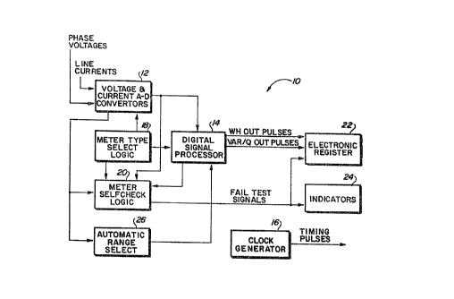
Reference is now made to Fig. 1, which is a major block
diagram of an electronic watthour meter shown generally at
10 in accordance with the present invention. The Deter 10
is connected to a power distribution service or network and
receives phase voltage inputs and line current inputs, which
19 11°ME-249
after having been scaled and isolated are provided to the
input of two Voltage and Current Analog to Digital (A-D)
Converters 12 for converting the voltage and line current
inputs to corresponding digital output words which are
provided to a Digital Signal Processor (DSP) 14. A Clock
Generator 16 generates a plurality of timing pulses from a
precision oscillator and provides those timing pulses to the
various blocks of the meter for controlling the operations
of the meter and the Processor 14. A Meter Type Select
Logic 18 is utilized to provide various timing signals to
the A-D Converters 12 and to the Digital Signal Pracessor 14
to control the operations thereof in accordance with the
configuration of the mater selected by Select Logic 18 to
correspond to the particular type of power service network
to which the meter is connected. The Meter Type Select
Logic 18 also provides control signals to a Meter Self Check
Logic 20 along with outputs of the A-D Converters 12 to
selectively effect the generation of fail test signals
representative of various operational conditions taking
place within the meter. These fail test signals are
provided to a plurality of Indicators 24 for instantaneously
showing t:he status of the meter and also to an Electronic
Register 22 such as a demand register or time of use
20 11-ME-249
register. The Electronic Register may be programmed to
monitor these fail test signals and display the status of
those signals, for example, on a liquid crystal display fox
use by a meter reader in analyzing the condition of the
meter. The A-D Converters 12 also provide digital words or
signals proportional to phase voltages and line currents to
the input of the Meter Self Check Logic 20 and to an
Automatic Range Select 26. The Self Check Logic 20 monitors
the signals proportional to the phase voltage inputs to
continuously check on the condition of the voltage sensors
and isolation networks feeding the voltages to the input of
the voltage A-D Converter. The Automatic Range Select 26
continuously monitors signals proportional to line current
inputs to the A-D Converters and, each analog to digital
conversion period of the input currents, will provide a
signal to the Digital Signal Processor 14, notifying it of
the selected range of input current.
The Digital Signal Processor, in response to a reset or
start signal from the Clock Generator 16 periodically reads
the outputs of the A-D Converters 12. The outputs of the
A-D Converters are read by the Processor at the termination
of each A-~D Conversion sample of the input phase voltages
and 1 ine currents .
21 11-ME-249
Thus, the samples provided to the Processor 14 are signals
representative of the value; of instantaneous voltage and
current provided to the meter. These voltage and current
samples are periodically multiplied in the Processor 14 and
integrated over a period of time to generate output pulses
designated as WH OUT and VAR/Q OUT pulses to the Electronic
Register 22. WH OUT or VAR/Q OUT pulse is generated each
time the integrated value achieves a prescribed threshold
level for the appropriate calculatian (ie, ~H and Var/Qj.
There is a threshold value stored in the digital signal
processor as a constant for each of the various meter types
selected by the Meter Type Select Logic 18. Tn the present
embodiment there are six different types of meters as will
subsequently be described which can be selected by Logic 18.
Thus the Signal Processor 14 stores a threshold constant for
each of the various types of meters. The rate of WH OUT and
V.AR/Q OUT pulses to the Register 22 is determined by the
threshold value for the particular type of meter selected by
Logic 18. A more detailed description of how the WH and
VAR/Q OUT pulses are generated will subsequently be
described.
~;~~~~fl~~
22 11-ME-249
Reference is now made to Fig. 2. The basic timing
signals for controlling the sequence of operations of the
invention axe generated by the Clock Generator 16 as shown
in Fig. 2. The Clock Generator is comprised of a high
precision Oscillator 28 which provides a 4.97 M~iZ signal
designated MCLK to the Digital Signal Processor (DSP) 14 and
to an A-D Clock Generator 30. The Clock Generator 30
divides the 4,97 MHZ clock signal down to a 207 XHZ signal
designated ADCLK. The ADCLK signal is provided to the meter
analog to digital converters and to a range select for
controlling the operations thereof in a manner to be
described. The ADCLK signals are also applied to a Time
Base Generator 32 which generates a plurality of output
timing signals designated FCCLK, RESET, V SAMPLE, and T
SAMPLE. The timing relationships of these signals along
with the ADCLK'signal will be subsequently described in
connection with the detailed operational description of the
invention.
~u~~.~~~
23 11-ME-249
Fig. 2 also shows a Precision Voltage Reference 34 for
generating a plurality of voltage references for use in the
electronic meter of the present invention. The manner in
which these references are applied will be subsequently
described in the detailed operational description of the
invention in connection with Fig. 3.
Reference is now made to Fig. 3 which is a detailed
logic schematic diagram of the electronic meter of the
present invention. However, prior to proceeding with the
detailed operational description of the invention, it is
believed first advantageous to describe the basic functions
and the purpose of the various logic elements and circuits
which make up the meter.
The mater of Fig. 3 is illustrated as receiving three
phase voltage inputs (Phase 1 - Phase 3j from a polyphase
power distribution service into a Voltage Scaling and
Isolation Circuit 36 associated with each of the individual
phase voltage inputs. The Voltage Scaling and Isolation
Circuits 36 provide electrical isolation from the power
lines and also scales down the various line voltages; far
example from 1.20 volts through 480 volts down to
i
~~~~1~ ~~
24 11-ME°249
approximately 1.6 volts for input to a voltage multiplexor
(VNIUX) 38. The voltage inputs designated VSA thru VSC are
multiplexed by the VMUX 38 t:o provide a multiplexed output
signal to a Self Check Enable Switch (SW 4~). The
multiplexing of the VSA through VSC voltage signals through
the VNiUX 38 is controlled by the timing of three clock
pulses VACLTC, VBLK, VCCLK which axe applied to the VMUX 38
from a Multiplexor Control (MiJX Control 42). The manner in
which the VMCTX is controlled by these latter clock signals
will subsequently be described.
The multiplex voltage signals are passed through SW 40
and applied to the input of a Voltage analog to digital (A-D
Converter 12'). Each voltage phase signal VSA through VSC,
as it is passed through the V1HUX 38 and SW 4~, is converted
during a sample time as controlled by a V SAMPLE signal
applied to the A-D Converter to thus generate digital output
signals in the form of a digital word shown as bits DVO~DVN
at the output of the Converter 12'. The output word from
A°D Converter 12° is applied directly as one input to the
Digital Signal Processor 14 (DSP) and also to the input of a
Voltage Tn Decode Circuit 44.
25 11-ME-249
The Voltage In Decode 44 continuously monitors each
digital voltage sample at the output of the A-D Converter.
So long as the magnitude of the digital word, as represented
by DVO-DVN, is above a prescribed magnitude or threshold, an
output signal VIIN from the Decode 44 will remain at a
binary 1 state at the input of the Voltage and Line
Frec,~uency Test Circuit 209' . Circuit 20'9 forms a portion of
the Meter Self Check Logic 20 as previously described in
connection with Fig. 1.
Reference is now made to the left bottom corner of Fig.
3 where it is shown that three line currents Line 1 - Line
3) are applied to three Current Scaling and Isolation
Circuits 46. In the preferred embodiment, the Current
Scaling and Isolation Circuits 46 each provide electrical
isolation from the power line and scales the line currents
down to approximately 2 milliamps maximum for input to a
Current Multiplexor ~IM~TX) 48. Typical input currents to
the Scaling Circuits 46 can be up to 200 amperes for
self-contained meters and up to 20 amperes for transformer-
rated meters. Three current test signals ITA-ITC are
provided to the self test logic 20'. During self check
operation these signals are monitored to test for a failure
in any of the Current Scaling and Isolation Circuits 46.
~;i~~ ~.~~)
2 6 11-~-2 4 9
Output current signaler ISA through ISC are provided to
the input of the IMUX 48 arid are multiplexed therethrough :in
a fashion similar to the V~IUX 38 by three clack signals,
IACLK, IBCLK and ICCLK from a Current Phase Clock 50. The
Current Phase Clock is clor;ked by the I SAMPLE signal from
the Tame Base Generator 32 to properly cycle the clock
signals IACLK - ICC7LK to control the multiplexing of 'the ISA
- ISC signals through the IMUX ~8 to thus provide a
multiplexed input signal IIN to the input of a Switched Gain
Control Circuit 52. The S~ritched Gain Control 52 comprises
a part of the Automatic Range Select 26 and automatically
provides a scaled up or scaled down IIN current signal to
the input of a Current to Voltage Converter 54. The current
signal from the Switch Gain Control 52 gets converted to a
voltage signal proportional to the magnitude of IIN in the
Current to Voltage Converter 54. This proportional voltage
signal gets passed directly to the Current Analog to Digital
(A-D) Converter 12a",via a Gain Adjust 56 and~a Self Check
Voltage Test.Switch 58.
The output of the Gain Adjust 56 is a voltage
proportional to the input current IIN and is designated as
TOUT. This IOUT signal is applied as one input to a Range
Select 60, also forming a part of the Automatic Range
27 11-ME-249
Select 26 previously descrilbed. The Range Select 60
receives the I SAMPLE and A;DCLK cl~ck signals from 'the Time
Base Generator 32 and monitors the IOUT signal to thus
provide a control signal designated EN1~ to the DSP 14 and
to the Switch Gain Control .52. The details for the Range
Select Circuit 60 will subsequently be described. However
for the present, suffice to say 'that that circuit
continuously monitors the magnitude of the LOUT signal and,
as the magnitude of that signal changes, the EN16 control
signal wall cause the Switched Gain Control 52 to scale the
input current IIN to the proper level for input to the
Current to Voltage Converter 54. As previously mentioned,
the purpose of this scaling is to properly scale up the
small signal levels of the input current IIN to be more
nearly comparable to large signals thus reducing the total
range over which the Current A-D Converter 12" must operate.
The EN16 signal from the Range Select 50 is a binary signal
which switches between a binary 0 and a binary 1. This
signal is monitored by the DSP 14 and is utilized
by the DSP to know which scaling is being.applied to the
input current IIN in order to make the proper calculations
when computing the values of watthours and Var/~ hours.
28 11-ME-249
The current A-D Converter 12'° also receives
input signals similar to the: Voltage A-D Converter 12' and
samples signals proportional, to the multiplexed input
current signals ISA - ISC to thus provide at its output
digital words corresponding in magnitude to the respective
samples of the analog input current. These digital words
are provided on a plurality of lines to the input of the DSP
14 designated as Signals DIO-DIN. As previously mentioned,
DSP 14 serves to multiply the .respective digital voltage and
current samples together to derive instantaneous power at
the time of each sample. Each digital sample DV'O-DVN and
DIO-DIN is clocked into the DSP 14 at the time of generation
of the RESET signal from the Time Base Generator 32 (see .
Fig. 2) .
The MCLK high frequency signal from the Oscillator 28
is also provided as the basic master clock for the input to
the DSp 14. P~IChK allows the DSP 14 to operate at a very
high frequency in comparison to the remainder of the meter.
This high frequency clocking, which is attributed to the
xCLK signal, allows the DSP to process a vast amount of data
between analog to digital samples as will subsequently be
described.
2~ 11-r~-z49
Still referring to Fig.. 3, the Nteter Type Select Logic
18 as previously described :in connection with Fig. 1 is
shown as being comprised of a Type Select 62, a Type Select
Decoder 64, a Threshold Decode 66 and the aforementioned MUX
Control 42. As previously mentioned, when the meter is
connected to the proper phase voltages and line currents for
of the particular type of service being monitored, the meter
of the present invention can be configured to measure energy
in two or three wire single phase circuits or
three or four wire polyphase circuits. The ananner in which
the meter of the present invention can be configured to
meter electrical energy from the above mentioned six
different circuits is best shown by reference to the
following Table 1.
3 0 1. 2-ME-2 4 9
TABLE 1
TYPE SELECT CODING BY METER TYPE
BIT2 BIT1 BITO TYPE DESCRIPTION BY APPLICATION
3-ELEMENT MhTER FOR FOUR-WIRE TYPE 1
0 0 1 THREE-PHASE WYE SERVICE
2-ELEMENT METER FOR FOUR--WIRE TYPE 2
0 1 0 THREE-PHASE WYE SERVTCE
2-ELEMENT METER FOR THREE-WIRE TYPE 3
0 1 1 THREE-PHASE DELTA OR THREEWIRE
NETWORK SERVICE
2-ELEMENT METER FOR FOUR-WIRE TYPE 4
1 0 0 THREE-PHASE DELTA SERVICE
1-ELEMENT METER FAR THREE-WIRE TYPE 5
1 0 1 . _ STNGLE PHASE SERVICE
1-ELEMENT METER FOR TWO-WTRE TYPE 6
1 1 0 SINGLE PHASE SERVICE
BIT3 DESCRIPTION
0 SELF-CONTAINED METER
1 TRANSFORMER-RATED METER
Table 1 shows the states of four binary bits; Bit 0,
Bit 1, Bit 2 and Bit 3. These bits correspond to Bits 0°3
as shown at the output of the Type Select 62 of Fig. 3. As
shown in Fig. 3, the Type Select 62 contains four sets of
terminal connections which can be jumpered to set up the
various binary bit configurations for input to the Type
Select Decoder 64 by merely connecting jumpers across the
various terminal connections. For example, when a jumper is
connected across a particular set of jumper terminals such
31 11°ME°2~9
as shown for Bit 3, then Bit 3 is considered to be a binary
1, whereas in the absence of a jumper, the bit will be a
binary 0. As can be seen from Table 1 it takes three unique
binary bits, Bits 0°2, to define the six different types of
meters by application. In addition a fourth, Bit 3, is
required to define whether the particular meter is a self°
contained meter or a transformer-rated meter as shown in the
second half of Table. 1. To configure the meter type for a
particular application die, service) it can be seen that it
l0 is only necessary to connect the appropriate jumpers in the
Type Select 62 to achieve the desired configuration. For
example as shown in Table 1, if the meter is to be
configured as a Type 1 for a four°wire three-phase wye
service, Bit 0 will have a jumper connected across its two
terminals, whereas Bits 1 ° 2 will be left open. Further,
if it is assumed that this Type 1 meter is a self-contained
meter, then terminal connections of Bit 3 will likewise be
left open. By observation of Table 1 in connection with the
Type Select jumpers in Type Select 62 it can be seen how the
various other meter types 2 through 6 can be selected.
The requirement to be able to distinguish between a
self-contained meter and a transformer-rated meter as set by
32 11-~E-249
Bit 3 of the Type Select 62 arises from the evolution of the
aforementioned induction type watthour meters where
transformer-rated meters generally run at a certain design
speed at a test current of 2.5 amperes
(out of a full scale of 20 amperes) and self-contained
meters run at the same speed at a test current of 30 amperes
(out of a full scale of 200 amperes). Ideally, in the
present invention, the electronic meter is designed to
exactly emulate existing induction type watthour meters by
providing watthour output pulses from the DSP 14 at a rate
exactly 12 times the speed of the eguivalent induction
watthour meter disc. Thus it can be seen that the DSP, in
order to be able to distinguish between in a self-contained
and a transformer-rated meter, must be notified of the
magnitude of the input current provided to the meter in
order to establish the proper threshold in the DSP 14 to
generate the watthour output pulses at the proper rate for
that particular input current. The manner in which the DSP
14 distinguishes between transformer-rated and the
self-contained meters will subsegczently be described.
Still referring to Fig. 3, the Bits 0-3 are applied to
the Type Select Decoder 64 wherein they are decoded into
four binary Type Select output bits designated TSBO through
TSB3.
~3 11-ME-249
The Type Select Decoder 64 decodes Bits 0°3 to provide the
proper type select bits TSBt~ - TSB2 to the MUX Control 42
for decoding therein to effa=ct the proper generation of the
Clock Signals VACLK-VCCLK ties the VMUX 3~.
The MUX Control 42 also receives the current clock
signals ~ACLK-ICCLK from the Phases Current Clock 50. The
MiJX Control 42 utilizes these latter signals in conjunction
with the decoding of the TSBO through TSB2 signals to
control the sequencing of the generation of the VACLK
through VCCLK signals which are applied to the VI~ITJX 38. The
Mux Control 42 also decodes the TSBO through TSB2 signals to
generate two signals EHB and ENC which are applied as inputs
to the Voltage and Line Frequency Test circuit 20°°.
Further, depending on the type of meter configuration, the
2iUX Control 42 also provides a divide by two signal ('2) to
the DSP 14.
Still referring to Fig. 3, the TSBO through TSB2
signals, including the TSB3 signal are also provided as
inputs to the Threshold Decode Logic ti6. This logic decodes
those input bits to thus generate three threshold identifier
bits THt7, TH1 and TH2 which are applied as inputs to the DSP
14. As will subsequently be described, the DSP decodes
these bits to make a determination as to which threshold to
34 11-ME-249
utilize for the particular type of meter being configured.
In addition, the Threshold Decode 66 decades bits TSBO -
TSB2 to provide two signals ENIB and ENIC to the Current and
DSP Self Test Logic circuit 20" to inform that logic of the
current inputs utilized for the type of meter configuration
being tested.
Reference is now made to a Self Check Switch 68 of Fig.
3. The Self Check Switch 68 is a push button switch which
is manually activated, far example, by a meter reader or by
a test technician, to apply a ground signal to a Self Check
Enable Logic Circuit 70. When the Self Check Switch is
closed, the FCCLK clock signal from the Time Base Generator
32 enables the Self Check Enable 70 to generate a Self Check
Enable Output Signal shown as SELFCHKEN. As previously
mentioned the meter of the present invention has a
capability of performing a self check on the operation of
the various critical circuits within the meter. Thus when
the SELFCHKEN signal is generated, that signal is applied to
the Current and DSP Self Test 20', the A-D Converter Test
Switch 58, A-D Converter Test Switch 40, the Isolation
Circuits 46, and to Threshold Decode Logic 66.
The Current and DSP Self Test 20° includes logic far
monitoring the states of the Current Test signals ITA-ITC.
During the self check period, that is when SELFCHKEN is
~i~~~i.~~l
35 11-ME-249
high, if any one of the ITA-TTC signals go high (To a binary
1), the TVC TEST signal is generated as an indication that
one of the Current Scaling and isolation Circuits 4s has
failed. This IVC TEST signal is provided as one input to
the Voltage and Line Frequency Test logic 20" at the top of
Fig. 3 and is combined therein with the DSP TEST and the
VIOUT signals to generate the SYSTEM FATL signal from the
output of the Voltage and Line Frequency Test 20".
Referring back to the Current and DSP Self Test logic
l0 20', it will be rioted that another output signal from that
logic is the DSP TEST signal, which is also applied to the
Voltage and Line Frequency Test 20". This signal is also
generated during the self check enable periad in response to
the WH OUT pulses which are applied to the Test Logic 20'
7L5 from the output of the DSP 14. The DSP Self Test Logic 20'
includes a timer counter which begins to count upon the
receipt of a first WH OUT pulse from the DSP 14. This timer
is enabled to begin counting during the period of the
SELFCHKEN signal. If the DSP 14 has riot generated a second
WFi OUT signal within a specified window period before the
timer times out, the DSP TEST signal will be generated as an
indication that the DSP 14 has generated a faulty signal.
36 11-ME-249
As previously described, the: DSP TEST signal is combined
with the IVC TEST and VIOUT signals in the Voltage and Line
Frequency Test Logic 20" to generate the SYSTEM FAIL signal.
Also this DSP TEST signal may be provided to the Electronic
Register 22 or the Indicators 24 as an indication of a DSP
failure.
Still referring to Fig. 3, reference is now made to a
VAR/Q Select Switch 72. As illustrated, this select switch
is a single pole single throw switch, which when closed,
applies a ground or logic 0 signal to a Varclock Generator
74 and DSP 14. Varclock Generator 74 also receives as a
clock input signal the IACLK signal from the Current Phase
Clock 50. The output of the Varclock Generator 74 is a
signal designated VARCLK which is applied as another input
to the DSP 14. The state of VARCLK is sampled by the DSP,
and its state, at the time of sampling, directs the DSP to
calculate either Varhours or Qhours. The VARCLK signal is a
binary signal which varies in accordance with the state of
the Var/Q Select Switch 72. The operation of the Varclock
Generator 74 and the manner in which VARCLK is modified in
accordance with the state of Switch 72 will become clear in
the ensuing description.
~~~~~~?
37 11~ME-2~9
Reference is now made rack to the voltage and Line
Frequency Test circuit 20°°. That signal generates a 60
Hertz line frequency output signal designated LFOUT which is
provided to the Electronic Register 22 as a timekeeping
pulse for that register. The LFOUT signal may also be
applied to one of the Indicators 2~ to indicate the presence
of the 60 Hertz input signal to the meter. The LFOUT signal
is also applied to a divide by 32 (~ 32) Counter 76 which
generates an output signal OFFCLK every 32 cycles of the
LFOUT signal. The OFFCLE signal is applied as another input
to the DSP 1~ and is utilized by the Processor as a flag to
cause it to enter into a DC offset subroutine to perform the
DC offset compensation previously referred to.
Prior to proceeding with a further detailed description
of the invention it is first believed advantageous to
provide a brief overall description of the operation of the
invention. For this description, let it be assumed that the
meter has been configured as a Type 1 for connection to a
four wire wye service as shown in Table 1. To adapt the
electronic meter of the invention to meter this type of
service requires the use of all three current inputs and all
three voltage inputs. Still referring to Fig. 3, the
current and voltage inputs must be connected such that 1SA
ss 11-~E-2~9
monitors Line 1, VSA monitors Phase 1, etc. The VMU~ 38
and the IMUX ~8 must be operated such that VSA is sampled
simultaneously with ISA, VSB with TSB, and VSC with ISC.
Each pair of samples (eg, I5A and VSA) gets converted to
digital words in the respective A-D converters 12' and 12",
multiplied in the DSP, summed and accumulated therein to
derive a calculation of energy.
In the DSP the multiplication of each set of current
and voltage inputs (VSAISA, VSBISB, VSCISC) calculates the
power contribution for each phase for each sample taken by
the respective A-D converters . The V~IITX and IPqUX are
controlled by the VACLK through VCCLK and IACLK through
ICCLK signals to sequentially sample each phase. By
sequentially sampling each phase, and adding the products
resulting from the multiplication of the current and voltage
samples into a common accumulator in the DSP 14 sums
together the power contribution of each phase. The
accumulation of all power samples over time integrates power
into energy. Each time the accumulator equals or exceeds the
value set by the aforementioned threshold for the particular
meter type selected, one output pulse (WH OUT) is generated
and the value of the threshold for that meter type is
subtracted from the accumulator. The WFI OUT pulse which is
generated is proportional to one quantum of energy
39 11°ME°249
flowing in the four wire wye circuit being metered in the
present example.
For each of the six msaer types previously described
and as shown in Table 1, appropriate sampling schemes and
corresponding threshold values have been established. The
following Table 2 shows a sampling sequence which is
employed for the various types of meters.
TABLE 2
SAMPLING SEQUENCE
vMUx IMUx
SEQUENCE METE12TYPE
~?~TE 1. 2 3 4 5 6
1 VSA VSA/2 VSA VSA/2 VSA/2 VSA ISA
2 VSB VSA ~* VSA/2 VSA/2 ~* ISB
3 VSC VSC/2 VSC VSC ~# ~# ISC
4 VSA VSA/2 VSA VSA/2 VSA/2 VSA ISA
5 VSB VSA g5* VSA/2 VSA/2 ~* TSB
6 VSC VSC/2 VSC VSC # ~# ISC
7 VSA VSA/2 VSA VSA/2 VSA/2 VSA ISA
8 VSB VSC ~* VSA/2 VSA/2 ~* ISB
VSC VSC/2 VSC VSC ~# ~p# ISC
20 VSA VSA/2 VSA VSA/2 VSA/2 VSA ISA
11 VSB VSC ~* VSA/2 VSA/2 ~* ISB
12 VSC VSCj2 VSC VSC cb# ~# ISG
* VSB and ISB DISCONNECTED
# VSC AND ISC diSCOnneGted
40 11-MS-249
The twelve sequence states shown represent twelve
sequential samples, where t;he quantity (eg, VSA) selected by
the VMUX 38 is multiplied by the quantity (eg, ISA) selected
by the IMUX 48. In Table 2, it will be noted that a zero
exists for certain of the voltage and curxent inputs such as
shown for meter types 3, 5 and 6. When these meter types
are configured, the respective phase voltages and line
currents as shown in Table 2 are disconnected, thus the
corresponding voltage and current input signals to the mater
are considered as zero. The manner in which the invention
handles the sampling of the zero inputs will subsequently be
described.
Still referring to Table 2, each of the sequence states
1 through 12 represents a sample of the respective voltage
and current inputs for the phases shown (eg, VSA, ISA,
etc.). Averaged over 12 sequential samples, it can be shown
that average power per sample is as summarized in the
following Table 3 for each meter type. Also shown in Table
3 are W, the power per sample in milliwattst f, the desired
output pulse rate (that is of WkT OUT)t and the corresponding
threshold value for each meter type given in milliwatts per
pulse. As previously mentioned, these threshold values are
stored as constants in the memory of the DSP 14. While each
~~~r~~~~l
41 11~ME-2~9
meter type has its own threshold value, it will be noted
that meter types 3 and 4 share the same threshold, and meter
types 5 and 6 likewise share a common threshold. Thus the
DSP need only store three separate threshold values, that
S is, separate values for meter types 1 and 2, a separate
value for meter types 3 and 4, and another value for meter
types 5 and 6.
TADLE 3
Vd F THRESHOLD
METER MILLIWATTSPULSE/SECMILLIIJATTS
TYPE POHERUATION (NOTE (NOTE /PULSE
EQ 1) 2)
1 )/3(VSA + VSBISB + .480 15/9 2B759
ISA VSCISC)
2 )/3(VSAISA+ VSAISB +VSCISB.320 20/9 13380
+ VSCISC
2 2 2 2
3 1/3(VSAISA+ VSC1SC) .920_ 15/9 17840
4 i/9(VSAISA+ VSA1SB + .32D 15/9 17840
VSCISC)
2 2
1/3(VSAISA+ VSAISB) .1B0 30/9 4460
2 2
6 1/3fVSAISA) .160 30/9 4460
NOTE l: Average power per sample at rated voltage (1.6V)
and test current (300 microamperes) ~ Unity power factor
NOTE 2: Output pulse rate for conditions of Note 1.
42 11~ME°249
The threshold value for each of the thresholds in Table
3 is calculated as follows:
Threshold = 128 mw/sample X W X 17280 samples/sec>
3.45X3.45 2F
= W X 92915 mw/pulse
F
Where: W = average power per sample at test condition
F = output pulse rate
17280 samples/sec =~ sample rate
3.45 Full scale reference voltage of each
converter
If W were at full scale on current and full scale on
voltage, then 128mW would be added to the DSP accumulator
for each sample. The term W/(3>45X3.45) determines what
portion of full scale is represented by each sample and in
turn, what portion of 128 will be added to the DSP
accumulator fox the sample. The 2F term is required because
twa internal states the DSP are required to generate one
output pulse.
The threshold values given in Table 3 are for
self-contained meters. To obtain the same output pulse
rats, F, at a test current of 250 microamperes instead of
the 300 microamperes used for Table 3, (see dotes 1 and 2)
involves simply reducing the threshold by the ratio of the
43 11-ME-249
test currents, by 5/6 (.83325). Therefore, as previously
explained in connection wi~:h Table 1, the fourth type select
bit (TSB3) which is used to select self-contained or
transformer-rated meters, need only effect a reduction in
the threshold value by a factor of 5/6 when a transformer-
rated meter is selected.
Continuing now with a further detailed description of
the invention, reference is now made to Fig. 4. Fig. 4 is a
basic timing diagram illustrating the timing relationships
between the various timing signals generated by the Clock
Generatar 16 as shown in Fig. 2. The ADCLK signal from the
A-D Clock Generator 30 is a 207KH~ clock signal which gets
divided down in the Time Base Generator 32 to generate the
respective output signals RESET, V SAMPLE, I SAMPLE, and
FCCLK. It will be noted that a RESET signal occurs every 12
ADCLK pulses. The interval between the RESET pulses
represents one cycle, or as previously described in
connection with Table 2, one sequence state. It will also
be noted that the time period between RESET pulses
represents one A-D conversion time, the time when each A-D
sample is taken and converted. In Fig. 4, for illustrative
and explanatory purposes, the VACLK-VCCLK and IACLK-ICCLK
signals are shown as being sequentially generated as
44 11-ME-249
previously described for a Type 1 meter (see Table 2) for
metering energy for a four wire wye service. The voltage
and current inputs to the A-D converters 12' and 12" from
the VtKtJX 38 and the IMCJX 48 are sampled during each of the
VSAMPLE and ISAMPLE pulse times as shown in Fig. 4. This is
the input acquisition time of each of the respective A-D
converters. when VSAM~LE and ISAM~LE are both at binary 1
states, the VACLX and IACLK signals are applied to the
respective multiplexors to switch the respective VSA and ISA
input voltage and current signals through the V34L1X and IiKiJX
under control of the MLTX Control 42 as shown in Fig. 3.
This sampling or taking of an A-D conversion of the VSA and
ISA input signals is shown as sampling phase A (~A) in ~'ig.
4. In a similar fashion, with the generation of each
VSAMPLE and ISA~iPLE signal, phases ~ B and rp C are
sequentially sampled. As can be seen in Fig. ~, the VACLK
and IACLK signals are 17.28 KHZ signals with one complete
time frame taking approximately 174 microseconds Shawn as an
overall frequency of 5.76 I~iZ. Thus, it can be seen that
each sample takes approximately 58 microseconds. At the end
of each A-D conversion cycle, the outputs from the A-D
converters 12' and 12°' (DVO-DVN and DI0-DIN), are read into
the DSP 14 (clocked at Reset time) as new carrent and
~~?~.Q~~
45 11-1ME°249
voltage values shown as IADC: and VADC in Fig. 4. The manner
in which the DSP 14 processca these values will be
subsequently described.
As previously mentioned, the multiplexing of the
VSA-VSC voltage input signa:Ls through the VI~IUX 38 of Fig. 3
is controlled by the sequencing of the VACLK-VCCLK signals
from the MTJX Control 42. The sequence of occurrence of the
VACLK-VCCLK signals is determined by a decoding in the MUX
Control Type Decode Circuit 42 of the type select bits
30 TSDO-TSB2. The sequence or times of generation of the
VACLK-VCCLK signals is dependent upon the meter type which
has been configured in the present invention.
Figs. 5-10 are timing diagrams of the operation of the
IKUX Control Type Decode 42 for the aforementioned meter
types 1-6.
Fig. 5, fox example, is a timing diagram of a Type 1
meter as previously described and it will be noted that the
timing is similar to that just described in connection with
Fig. 4. To achieve the sequential generation of the signals
VACLK-VCCLIC as shown in Fig. 5 to sequentially multiplex the
VSA-VSC signals through the VMUX 38 (Fig. 3) the type select
bits TSgO-TSB2 must have the states as shown in Fig. 5. The
states of TSDO-TSB2 correspond to the Type 1 meter
~s m-~E-a~9
as previausly described in connection with Table 1.
Further, it will be noted by referring to Table 2 that the
sequential sampling of VSA-VSC by the VACTaK-VCCLK signals
corresponds to the sequence states as previously described
in connection wa.th Table 2. These twelve sequence states
are as numbered above the VSA~PI~E line in Fig. 5 and Figs. 6
through 10. It will also be noted in Figs. 5 through 10
that the sequential timing of the IACLK-ICCLIC signals is not
altered. As can be seen in Fig. 3, the only input signal to
the Current F~hase Clock 50 is the ISAMPLE signal which
occurs simultaneously with the VSAMPLE signal applied to the
MUX Control 42. There are no input control signals or any
decode required in the Current Phase Clock 50. Thus it
merely generates the signals IACLK-ICCIaK sequentially as
shown in each of the timing diagrams Figs. 5 through ~Ø
Still referring to Fig. 5, it can be seen that during
sequence state 1, the VSA and ISA (VA and IAA input signals
are simultaneously sampled by their respective A-lD
converters as controlled by the states of the IACLK-ICCLK
signals applied to the IMUX 48 and the VACLK-VCCLTZ applied
to the VM~TX 38. In a similar fashion during sequence states
2 and 3, VSE and ISB and VSC-ISC are sequentially sampled.
~~~~~~~3~~~
47 11-ME-249
Reference is now made 'to Fig. 6 which is a timing
diagram for the Type 2 meter showing the generation of the
VACLI~-VCC~IC signals from the MUX Control 42. Reference is
also made back to Tables 2 and 3 where it will be noted that
for a Type 2 meter, the quantities VSA and VSC must be
divided by 2 to derive the proper product in the DSP for the
VSA and ISA and VSC and TSC samples. Further, it will be
noted as shown in Table 1 that a Type 2 meter is a 2 element
meter for a four wire three phase wye service, thus that
meter does not monitor the VSB voltage phase input. This
non-monitoring is accomplished as shown in Fig. 6 by the
decodes of the states of the TSBO through TSB2 signals in
the MUX Control 42. As shown the VBCLK signal is not
generated for a Type 2 mater, thus the VSB signal is not
multiplexed through the MUX 38. It should be noted,
however, that the meter does monitor the ISB current signal
applied to the IMUX 48. ISB gets converted simultaneously
with either VSA or VSC as shown in Fig. 6.
It is significant at this time to note in Fig, 6 that
the deCOde Of the TSB(-TSB2 SlgnalS alSO effeCtS the
generation of the = 2 signal from the output of the M~7X
Control 42 which is applied to the ASP 14. This latter
48 11-ME°249
signal notifies the DSP to divide certain of the VSA and VSC
samples by two to derive the equations as shown in Table 3.
Reference is now made to Fig. 8 which is a timing
diagram of a Type 4 meter. Further, reference .is made to
Table 1 which also indicates a Type 4 meter is a two element
meter similar~to Type 2 except it is configured fox a four
wire three phase delta service. As shown in Table 2 and in
Fig. 8 for this type of meter, the VSA input voltage signal
gets divided by 2 twice. Once during the first sequence
state when VSA and 3SA are sampled, and a second time during
the second sequence state, when VSA is sampled with zSB.
Reference is now made to Fig> 9 which is a timing
diagram of a Type 5 meter. The timing for the Type 5 meter
is similar to that as shown for the Type 4 meter except as
will be noted in Table l, the Type 5 meter is a single
element meter for a three wire single phase service. 1n
this type of service, there is only one voltage phase, VSA
to be monitored. However, there are two current phases, ISA
and 3SB which get metered. As shown in Fig. 9, VSA gets
divided by 2 twice as previously described and shown for the
Type 4 meter in Fig. 8. Further, it is significant to note
4~ 11-ME-249
that the input voltage and current signals VSC and ISC are
zero by virtue of the fact that those two inputs to the
meter are disconnected as noted in Table 2. Thus, during
the sequence state 3, when the A-D conversion is taking
place, the outputs of the A-D converters 22' and 22" are
both zero for VSC and ISC respectively.
Deference is now made to Fig. 20 which is a timing
diagram of a Type 6 meter as shown in Table 1, that meter is
a single element meter for a two wire single phase service.
In this type of meter there is only one voltage phase
connected to the meter, and that is VSA. Thus as shown in
Fig. 10 and in Table 2, when TSBC-TSB2 are configured t~
select a Type 6 meter, the VSB, ISB and VSC, ISC conversions
are zero which get read into the DSP 14.
25 Having described the operation of the PZUX Control Type
Decode 42 in connection with the Decoding of the TSBO-TSB2
signals as shown in Figs. 5 through 20, it is believed that
one using the timing diagrams Figs. 5 through 10 can readily
design the necessary decode logic to generate the
VACLK-VCCLK signals in a sequence as shown in those diagrams
and as described. It should be noted that when the DSP test
is initiated, the SELFCHIZEH signal will go high. When
SELFCHItE;N is high, the PZLJX Control Type Decode 42 will
unconditionally force the ~ 2 signal to the DSP 24 to remain
5~ 11-ME-249
low. This will cause the D:'P 14 to never divide by two
during the DSP test, independent of the particular meter
type selected.
Reference is now made back to Fig. 3 to the Threshold
Decode 66. As previously d~ascribed, the Threshold Decode
decodes Bits:TSBO-TSH3 from the Type Select Decoder 64 to
generate threshold decode output signals THO-TH2 which are
transferred to the DSP 14. The following Table 4 shows the
logic of the Threshold Decode 66 in equation form. Table 4
also shows how the DSP decodes the TIi2 output from the
Threshold Decode to make a determination as to whether the
configured meter is either transformer-rated or
self-contained. This Table also shows how the DSP decodes
the THO and TH1 outputs from the threshold decode to select
the proper threshold in its memory for the particular type
of meter that has been selected. It should be noted that
when the DSP self test is initiated, the SELFCHI~EN signal
will go high. When SELFCHICEN is high, the Threshold Decode
Logic 66 will unconditionally force TRIO through TH2 signals
to go low. This will cause the DSP 14 to select a
particular known threshold value for the DSP test,
independent of the particular meter type selected. The
manner in which the DSP decodes the THO through TH2 signals
will subsequently be described in connection with the
operational description of the DSP.
51 11-ME-249
TABLE ~
THRESHOLD SELECT DECODE LOGIC
FOR METER Z'YPES 1-6
TH1 - (TSBl . TSBO) + (TSBO . TSB1 . TSB2)
THO ~- (TSBI . TSB2) -t- (TSBO . TSB1)
TH2 TSB3: Transformer-rated meter. Reduce
=
selected threshold in DSP by 5/6 (.83325)
for particular meter type.
TH2 TSB3: Self-contained meter. UsE selected
=
threshold in DSP for particular meter
typeo
THO TH1 Select Threshold (26759) in DSP for
. :
Type 1 meter.
THO TH1 Select Threshold (13380) in DSP for
. :
Type 2 meter.
THO TH1 Select Threshold (1740) in DSP for
. :
Types 3 and 4 meters.
THO TH1 Select Threshold (4460) in DSP for
. :
Types 5 and 6 meters.
52 11-ME-249
The Threshold Decode 6S also decodes Bits TSBO-TSB2 to
generate two output signals ENIB and ENIC which are applied
to the Current and DSP Self Test logic 20°. The logic for
decoding these signals is shown on the following Table 5.
TABLE 5
METER TYPE DECODE LOGIC ~'OR
IVC TEST
Types 1 & 5 Type 2 Type 4
ENIB .- (TSBO . Tssl) -~ (TSB2 . TssO) + (TSBO . TsBl)
Types 1,2,&3 Type 4
ENIC - (TSB2) + (TSBO . TSB1)
~1s can be seen in Table 5, signal ENIB gets decoded as Types
1, 2, 4 and 5 and signal ENIC gets decoded as types 1, 2, ~
and 4. The ENIB and ENIC signals are utilized in the
Current DSP Self Test logic 20° only for the testing for the
failure of the sensors in the current Scaling and Isolation
l0 Circuits 46 as detected by the ITA-ITC signals applied to
the Self Test Logic 20'.
~~u ~'~.~0'~
53 11-MB-2~9
4ahen the meter has been configured to one of the types
of meters not using or moni3:oring current ISB or ISC, it is
necessary to disable testine~ of the particular line current
input in order to prevent the generation of a false current
test. The ENTB and ENIC signals enable the current and DSP
self test logic 20' to distinguish between the various types
of meters to prevent such generation. The ENIB signal from
the Threshold Decode 66 is ANDED in the Self 'test Logic
20~with the ITB signal. In a similar fashion, the ENIC
signal is ANDED with the ITC signal. When the ENIB signal
is enabled, it will allow its corresponding STD gate to be
enabled when the ITB signal goes high to detect a failure in
the line 2 current sensor. In a similar fashion, when the
ENIC signal is enabled it will allow its STD gate to be
enabled when the ITC signal goes high to detect a failure in
the line 3 current sensor. The outputs of the above
mentioned two ~3D gates are ORED together in an OR gate with
the ITA signal in the Test logic 20' to thus provide an
output signal from that gate whenever any one of the ITS-ITC
signals indicates a current sensor fail condition. The
output of that 012 gate serves to generate the IVC TRST
signal if there is a failure during the selfcheck period.
CA 02021092 1999-11-25
54 11-ME-249
Prior to proceeding with a further detailed description
of how the IVC TEST signal is generated, reference is now
made to Fig. 25 for a description of how the ITA-ITC signals
are generated in the Current Scaling and Isolation Circuits 46.
s Fig. 25 is a schmo~atic diagram of the Current Scaling
and Isolation Circuit 46 for sensing the Line 1 Current of
Fig.3. Similar Circuits 46 are present for Lines 2 and 3
currents.
U.S. patent 4,970,459 issued Noveanber 13, 1990 assigned
io to the assignee of the present application and entitled
Electronic Meter Chopper Stabilization discloses that portion
of the circuit of Fig. 25 c~rised of a current transformer
(CT), Switches 78, an Operational Amplifier 80 and a Current
Multiplexes 48.
i5 As part of the Self Check feature of the present
invention, a S'tniitch (SW) 84 and a Coa~arator 86 have been
incorporated into the circuit of Fig. 25. The Switch 84 is
operated by the SEI~~T signal to inject a Voltage Signal
of Irnown polarity into the negative (-) terminal of
ao Amplifier 80 when the meter is in the self check anode. This
55 11-N!E-249
voltage signal is provided by small current from a Current
Source 88 connected between the -VT reference and SW 84.
The output of Amplifier 80 on Conductor JO to a
positive (+) input terminal of a Comparator 86. The
negative (-) terminal of Comparator 86 is connected to the
-~VT reference (see Fig. 2).
The Switches 78 are driven by the FCCLI~ clock signal, at
an approximate 154 BIZ rate to continuously (alternately)
switch the potential of a sense winding Ns at the CT across
the positive and negative input terminals of Amplifier 80.
The output of Amplifier 80 is fed back through the contacts
of Switches 78 to a feedback winding Nf of the CT. This
feedback signal, through the Nf winding, nullifies the flux
in the core of the GT and reduces the voltage induced in the
Z5 Ns winding.
The Switches 78 also switch the polarity of the Nf
winding at the output of the Circuit 46~to thus provide the
aforementioned ISA current to the input of the INtUX 48. The
TMLJX also receives the current signals TSS and ISG from the
respective Current Tsolation and Scaling Circuits 46 as
shown in Figs. 25 and 3. The ZIN signal is shown in Fig. 25
at the output of the IMLIX 48. As previously described, this
signal is applied to the Switched Cain Control 52 (see Fig.
).
56 11°ME°249
Still referring to Fig. 25, let it now be assumed that
the SELFCHKEN signal is high (ie, in Test mode) causing SW
84 to apply the ITEST Current signal to Amplifier 80. The
magnitude of this signal at the negative input terminal of
Amplifier 80 does not have any affect on its operation so
long as the Ns or Nf windings are not open. Thus, the
output voltage of the amplifier is sufficiently low to
prevent turning on Comparator 86.
Let it now be assumed that the Current Sensor (CT) has
failed due to an opening in the Ns winding either during or
prior to entering into the Self Check mode. With the Ns
winding open, its polarity can no longer be switched by
Switches 80 across the amplifier input terminals. As a
result, the voltage caused by the ITEST current at the
negative terminal of Amplifier 80 drives it into saturation
causing its output to go positive, thus turning on the
Comparator 8S. When Comparator 86 turns on its output
signal ITA goes positive, thus providing an indication of
current sensor failure.
As previously described in connection with Fig. 3, the
ITA°ITC signals from the Current Isolation and Scaling
Circuits 46 are applied to the Current and DSP Self Test
Logic 20° where they are ORED together to generate the IVC
TEST signal. Reference is now made back to Fig. 3 for a
continuec! description of the Test Logic 20'.
57 11-ME-249
As previously mentioned, the Current and DSP Self Test
logic 20' also generates the DSP TEST signal whenever the
DSP 14 fails to generate the WH OiJT pulses within a specific
time window.
To best understand the operation of the Current and DSP
Self Test Logic, reference is now made to Fig. 12. which is
a timing diagram of the operation of that logic for the
generation of the IVC TEST and DSP TEST signals. Self Check
begins when the Self Check Switch 68 is depressed, at which
time the SELFC~3KEN signal goes high. The SELFCFTKEN signal
is latched on the rising edge of the FCCLK signal as shown
in Fig. 12. The SELFCHKEN signal will remain high for
different periods - depending on various conditions to be
explained. The states of the ENTE and ENIC signals will be
positive or negative according to the type of meter which
has been selected by the Threshold Decode 66. The basic
equations for the ENIB and ENIC signals are as previously
given in Table 5. As previously explained, these signals
identify to the Test Logic 20' the current sensor circuits
' to be tested.
It will be noted that the IVC TEST and the DSP TEST
signals are both low upon entering the test cycle. During
the test cycle, the ITA-ITC signals (see Figs. 3 and 25)
58 11°ME°249
will be tested for failure of a current sensor (CT of Fig.
25). The DSP is also tested by checking for WH ~UT pulses
from the DSP during the test cycle. The manner in which the
DSP generates the WH OTJT pulses for DSP Test will
subsequently be described.
Reference is now made to Fig. 12 in conjunction with
Figs. 3 and 25. As shown in Fig. 12, when the SELFCHKEN
signal goes high, the VTEST signal from the Precision
Voltage Reference 34 is switched via Switches SW 40 and SW
58 into the A°D Voltage and Current Converters 12' and 12"
as shown in Fig. 3. At this time both converters go through
the conversion process as previously described. Also at the
time the SELFCHI~N signal goes high, the ITEST current
signal as shown in Fig. 25 is switched into the negative
input terminal of Amplifier 80 via SW 84. Thus it can be
seen that the test current from the ° VT reference supply is
now applied to the input of Amplifier 80 to test for an open
sensor as previously described in connection with Fig. 25.
It will also be noted that the SELFCHk~EN signal is
applied to the input of the current and DSP Self Test Logic
20' as shown in Fig. 3. Thus at this time, as shown in Fig.
12, the FCCLW pulse starts to cloak a Self Check timer
inside the DSP Self Test Logic 20'. This timer, not shown,
is clacked.by FCCLK each time it goes positive.
a~ 11°ME-249
Upon entry into the teat mode, any one of the current
sensors in the Current Sca7.ing and Isolation Circuits 46
could have failed prior to entry into the test or one of
those sensors could fail during the test. For explanatory
S purposes, as shown in Fig. 22, on the IVC Test line, it will
be noted that the IVC Test signal is shown as going high
during the test period thus indicating that one of the
current sensors has failed as previously described in
connection with Fig. 25. For example, if the current sensor
in the Current Scaling and Isolation 46 has failed as
previously described in connection with Fig. 25 on the Line
1 current line, the ITA signal will be high and applied to
the input of the Curre';snt and DSP Self Test Logic 20'. As
previously described, the ITA signal is ORED with the ITB
and ITC signals in the Self Test Logic 20' to thus generate
the IVC TEST signal at the output of the Test Logic 20'. Of
course, at the time of the test and during the test, if none
of the ITA ~°ITC signals goes high, there will be no failure
detected and thus the IVC TEST signal will remain low as
shown in Fig. 12. The IVC TEST signal can come high at any
time during the Self Test cycle.
Reference is now made to the DSP TEST line of Fig. 12
wherein it will be noted that the DSP TEST signal will
60 11-ME-249
remain low all during the DSP Test cycle. It will be
recalled that the A-D conversions began at the very
beginning of the Self Check period. As previously described
in connection with Fig. 4, and A-D conversion sample only
takes approximately 5~ microseconds. And a~t the end of that
conversion sample, the outputs of the A-D converters are
cloaked into the digital signal processor for processing
therein. The processor operating in a very high frequency
from the MCLK pulse from the Clock Generator 16 can perform
many of these A-D conversions in a very short period of
time.
If the DSP 14, voltage A-D Converter 12' and Current
A-D Converter 12'° are operating properly, it will generate a
WH OUT pulse as shown in Fig. 12 within a prescribed period
of time following the start of the Self Check Test. The DSP
Self Test Logic 20° waits for the receipt of the first WH
OUT pulse from the DSP 14. However, if the DSP is not
operating properly, it may not generate any WH OUT pulse to
be detected by the Logic 208. For explanatory purposes as
shown in Fig. 12, the first WH OUT pulse is shown as being
generated by the DSP 14 at some time after the beginning of
the Self Test cycle. When the first WH OUT pulse is
received in the Test Logic 20' as shown in Fig. 12, that
pulse starts a DSP Test timer within the Logic 20'. The
~~rv:~~
61 11-ME-249
receipt of this first pulse gets latched iota a memory
within the Logic 20° to thus allow the DSP timer to be
clocked with the RESET pulse. The DSP Timer will continue
to count for a prescribed period of time, as shown in Fig.
12, at which time the output of the timer will go negative
to establish a WH OUT time window. This time window will
last a predetermined period of time until the DSP Test Timer
times out by going positive as shown in Fig. 12.
As shown in Fig. 12, a second WH OUT signal is received
during the 'i~H OUT window. If the DSP generates this second
WH OUT pulse within the window, it is an indication that the
DSP and converters are operating properly. Thus, as shown
at the top of Fig. 12, the SELFCHKEN signal is driven
negative to thus end the Self Check eycle. The Self Check
Enable signal, SELFCHKEN, is driven negative as shown in
Fig. 12, by an ENDSELFCHK signal generated at this time from
the DSP Self Test Logic 20°. This latter signal is applied
to the Self Cheek Enable Logic 70 to 'thus drive the
SELFCHKEN signal negative. On the other hand, if the second
WH OUT pulse is not received in the Test Logic 20°, the
ENDSELFCHK will not be generated and the SELFCHKEN signal
will remain high as shown by the dotted line in Fig. 22.
Assuming that the second WEi OUT signal has not been
received, the DSP Timer will continue to be clocked
62 11°ME°249
by the RESET pulse until it times out by going positive as
shown in Fig. 12. At this 'time, the DSP TEST signal goes
high as shown in Fig. ~.2 to indicate that the DSP test has
failed by virtue of the fact that the second wH oUT signal
was not received within the time window. Also at this time,
the SELFCHKEN signal is driven negative to end the Self
Check at the time the DSP Timer times out and at the same
time, stop the Self Check Timer. 1~t this time, of course,
the ENDSELFCHK will go positive to thus disable the
30 SELFCHKEN signal in the Self Check Enable Logic 7D.
Reference is now made to the SELFCHKEN line of Fig. 12
at the right hand side. There shown is a note that says End
Self Check on Self Check Timer out. It will be noted at
this point that the SELFCH~N signal goes negative to end
the Sslf Check. Tf the Self Check Timer were not allowed to
time out, there would be no way to terminate the self check
test period in the event that the DSP did not generate any
WH OUT pulses. This is due to the fact that if the first t~Fi
OUT signal is not received, the DSP Timer will never be
started and thus there will never be a DSP Timer time out to
terminate the Self Check.
63 11-ME-249
The operation of the voltage and Line Frequency Test
Logic 20" of Fig. 3 will now be described by reference to
Figs. 11 and 17. Referring first to Fig. 1'7, it will be
nated that the logic of the Voltage and Line Frequency Test
Circuit 20" generates all of the aforementioned output
signals, LFOUT, OFFCLK (from the :- by 32 Counter 76), the
VIOUT signal, and the SYSTEM FAIL signal. Further, it will
be noted that the input signals VACLK-VCCLK, FCCLE, VIIN,
and ENB and ENC, axe provided to that logic as previously
described in connection with the description of the Voltage
and Line Frequency Test Circuit 20" of Fig. 3.
Three 26 millisecond timers, 90, 92 and 94,
corresponding to the Voltage Input Phases VSA, VSB and VAC,
respectively are provided. These timers are each clocked by
the FCCLK signal which is applied t~ a DE input terminial for
each of the timers. The FCCLK signal gets inverted through
an Inverter 96 to provide a FCCLK signal to one of the DE
terminals of,.each of the timers to cause those timers to be
clacked in a conventional counter manner. Three flip-flops
98, 100 and 102, are also provided for controlling the
resetting of the Timers 90-94 and further for providing
signals FA, FB and FC to a Line Frequency Out Decode Logic
104.
~~i~:l~~~
64 11-M~-249
Each of the flip-flops 98, 100 and 102 are clocked by
the VACLK, VBCLK, and VCCLK signals respectively. As
previously described, the VIIId signal is applied to the
Voltage and Line Frequency Test Logic 20" from the Voltage
in Decode 44 as shown in Fig. 3. The VIIN signal from the
Voltage in Decode 44 is a binary signal which varies between
binary 0 and binary 1 dependent upon the magnitude of the
word from the Voltage A-D converter during each conversion
sample as the input voltages VSA, VSB and VSC are sampled.
For example, at the termination of each A-D conversion, the
magnitude of the output word from the Voltage A-D Converter
12' will have some binary value representative of and
proportional to the magnitude of the Fhase Voltage (VSA-VSC)
just sampled and converted. If the magnitude of this word
as decoded by the Voltage in Decode 44 is above a prescribed
threshold, the VIItd signal will be positive to thus apply a
positive input signal to each of the DE input terminals of
' the flip-flops 98-102. It will be noted that the VACLK,
VBCLK, and VCCLK clock signals are applied to the C or clock
input terminal of flip-flops 98, 3.00, and 102 respectively.
Thus it can be seen that each of the flip-flaps 98-3.02 will
capture the state of the VIIN signal open the occurrence of
the respective clock signals VACLK-VCCLK applied to those
flip-flops..
6 5 11-~iE-2 4 ~
The Q outputs of flip~~flops 100 and 102 are applied
as one input to two HAND Genes 104 and 106, respectively.
Gate 104 receives at its other input the ENB signal and Gate
106 receives at its other input the ENC signal. The ENB and
ENC signals are also applied to the Line lFrequency Decode
104. The ENB and ENC signals are utilized to either enable
or disable the operation of the Timers 92 and 94 depending
upon the type of meter which is selected by the MUX Control
42. The following Table 6 provides the logic equations
defining the logic for decoding the ENB and ENC signals in
the MtlX Control 42.
. TABLE 6
METER TY1~E DECODE FOR VIOUT
TEST
Type 1
ENB = TSBO .TSB1 . TSB2
Types 1-4
ENC = TSB2 + (TSBO . TSBIj
66 1.1-ME-249
Reference is now made to Fig. 11 which shows that the
VIIN signal can be either a binary 1 or binary 0. Assuming
that the VSA Phase Voltage input is being sampled upon the
occurrence of the VACLK signal and that VIIN is positive,
the flip-flop 98 will be set to thus cause its Q output
terminal to go positive to a binary 1 to thus apply a Reset
signal to the Timer 90, keeping that timer from running.
This binary 1 signal is designated as VSA and is also
applied to the Line Frequency Out Decode 7.04. On the other
30 hand, at the time of sampling the VSA Phase Voltage Input,
if the VI7:N is at a binary 0 or low state, the flip-flop 98
will be reset upon the occurrence of .the VACLK signal, thus
causing flip-flop 98 to reset. The Q output terminal of~
flip-flop 98 now goes to a low or binary 0 state, thus
removing the Reset signal from Timer 90. As shown in Fig.
11, when the Reset signal is removed from Timer 90, the
FCCLK signal will now toggle the Timer 90 to start the timer
as shown in Fig. 31. So long as flip-flop 98 remains reset,
the Timer 90 will continue to count the FCCLK signals. If
the flip-fl~p 98 is not set before the Timer 90 times out,
thus indicating a loss of the VSA input, the Q output from
Timer 90 will go to a binary 1 state and generate a VAT
signal avo shown in Fig. 17 which gets applied to the Line
Frequency decode 104 and also as one input to an OR Gate
108.
~~~xfl~~
67 11-ME-249
It will be noted that OR Gate 108 receives three inputs, the
VAT input, a VBT input, and a VCT input, the latter twa
coming from Timers 92 and 94. Thus it can be seen that
anytime one of these signa.l.s goes to a binary 1 state, OR
Gate 108 will be enabled to thus provide a binary 1 VIOTJT
Voltage Failure signal as previously described and as shown
in Fig. ~.
The other Timers 92 and 94 function in the same manner
as that just described for Timer 90 in response to
flip-flops 100 and 102, monitaring the VSB and VSC voltages
in accordance with the phasing of tine VBCLK and VCChK. It
is to be noted however, that the Timers 92 and 94 which
correspond to the VSB and VSC signals are also controlled at
their Reset inputs by the states of the ENB and ENC signals
applied to NAND gates 104 and 106. As can be seen from the
equations in Table 6, when the ENB signal is a binary 1 or
positive, NAND Gate 104 will be enabled to have its output
go negative to remove the Reset signal from Timer 92 when
the flip-flop 100 is in the Reset state: Of course, as
previously described for flip-flop 98, flip-flap 100 will
achieve a Reset state at the time of the VBCL1C signal if
VIIN is at a binary 0 or low state, thus indicating a loss
~s 11-~E-2 49
of the VSB input phase voltage. Should this occur, the Q
output of flip-flop l00 will go to a positive state and with
ENB at a positive state, a NAND Gate 104 will be enabled to
thus remove the Reset input from Timer 92. Timer 92 will
now begin to count the FCCThK pulses in the same manner as
previously described for Timer 90. The Timer 94 is reset in
the same fashion as described for Timer 92 when the FNC
signal is at a binary 1 state.
Tt can now be seen how if any one of the Voltage Phase
inputs VSA-VSB fails for a prescribed period of time as
determined by each of the 26 millisecond Timers 90-94, that
the VAT-VCT signals applied to ~r Gate 108 will enable that
gate to immediately generate the VIOUT signal representative
of one af, either a loss of one of the phase voltages, or
the possible failure of the Voltage A-D converter. As shown
in Fig. 11, each of the Timers 90-94 are started at a time
determined by the VAChK-VC~LK signals clocking the
respective flip-flops 98-102. Thus it can be seen that each
of these timers will be started at different times and thus
they will each time out at a later time to generate the
respective VAT-VCT signals.
Referring now to Fig. 17, it will be noted that the
V10UT signal is applied as one input signal to an oR Gate
~~~~~1~
69 11-ME-249
110. It will be noted that: other inputs to OR Gate 110 are
the DSP TEST and IvC TEST :>ignals from the Current and DSP
SelfTest Logic 20'. Thus ~.t can be seen, if the meter fails
either the voltage test (v7:0UT high), the DSP TEST or the
IvC TEST, OR Gate 110 will be enabled to provide a binary 1
high signal as one input to an AND Gate 112. The other
input to this latter gate is the SELFC~i%EN signal. Thus,
when the meter is in the self checl~ mode, Gate 112 will be
enabled to generate the SYSTEM FAIL signal if any one of the
aforementioned tests fails.
Reference is now made to the Line Frequency Out Decode
104. The logic for Decode 104 is shown in equation form in
the following Table 7.
TADLE 7
LF OUT DECODE I~C3~GaC
VSA Present vSA Missing
LFOVT = (vAT~~A~ + (F~~vA~~v~T~EN~) +
VSA & VSD Missing
(FC~vAT~vcT~ENC)~(EN~+v~T)
~~2.~~~
7 0 11-ME-2 4 9
The FA, FB and FC signals from Flipflops 98, 100, 102
are each at a frequency of approximately 60 Hertz. As can
be seen from the equations of Table 7, the logic of the
Decode 104 is designed such that if the VSA phase voltage is
missing, the frequency of the VSB phase voltage (ie,
frequency of FB) will be provided as LFOUT from the Decode
Logic 104. if neither VSA or VSB voltages are present, the
VSC voltage frequency will appear at the output of the
Decode Logic 104. Of course, if all of the phase voltage
inputs VSA-VSC are missing, the output signal LFOUT will not
be present.
Thus it can be seen from the above description of the
Line Frequency Out Decode 104 that the LFOUT signal, which
gets provided to the aforementioned Electronic Register 22
as a tame base signal for that register, will always be
provided so long as at least one of the phase voltage inputs
VSA-VSC is present at the input of the meter.
Still referring to Fig. 17, reference as now made to
the s 32 Counter 76 an conjunction with Fig. 16 which shows
2o the timing far the OFFCLK signal generated by that counter.
As shown in Fig. 16, the Counter 76 divides the LFOUT 60
Hertz signal down by 32 to thus generate a pulse output on
each 32 counts of the counter. As previously mentioned an
connection with the description of Fig. 3, this OFFCLK pulse
is provided to the DSP 14 and is utilized to set a flag an
the DSP 14_to notify the processor to enter the update DC
Offset subroutine. The manner in which the OFFCLK pulse is
~~~~~~1
71 11-ME-249
utilized in the DSP will subsequently be described.
Reference is now made ~>ack to Fig. 3 to the.Varclock
Generator 74. As previously mentioned the Varclock
Generator operates in response to the TACLK signal to
generate a repetitively occctrring output signal VARCLK which
is applied to the DSP ~.4. The Var/Q Select Switch 72
applies a select signal to the Varclock Generator shown as
VAR/QSLCT which is also applied to the DSP 14. Further, as
previously described, voltage words in the DSP are delayed
by the time equivalent to 90 degrees of the power line
frequency before multiplication by the current words. In a
similar fashion, when Q is selected by the VAR/Q Select
Switch 72, voltage words are delayed by 60 degrees of the
power line frequency before multiplication by the current
words. In the DSP,~products of the current and delayed
voltage are separately accumulated until the aforementioned
threshold is reached for the particular type of meter
selected. Thw aforementioned output pulses VAR/Q OUT are
provided from the DSP 14 to the aforementioned Electronic
Register. The VAR/QSLCT signal notifies the processor
whether to calculate Varhours or Qhours. The VAR/QSLCT
signal modifies the rate of the timing signal VARCLK as
shown in 1E'ig. 15. '6~hen Varhours are selected (VAR/QSLCT
low), VARCLK operates at 1/3 the frame rate, where the frame
rate is a;s previously described in connection with the
72 11°ME-2~9
timing diagram of Fig. ~. It will be recalled that a frame
is the time period required for the multiplexors VMUX 38 and
IMUX 48 to sequence through all three of the VSA°VSC, and
ISA°ISC inputs once. As shown in Fig. 15, VAFtCLK operates
at 1/2 the frame rate where Qhours are selected (VAR/~SLCT
high) .
The DSP 1~ samples the VARCLK signal and depending upon
its state at the time of sampling will control the time
delay of the voltage words. In the T~SP memory, there are
eight memory locations provided for Phase 1 voltage words
(VSA), eight for Phase 2 voltage words (VSB), and eight for
Phase 3 voltage words (VSC). hacks time the VARCLK signal
goes high, a new set of voltage words are loaded into
memory, those already in memory are shifted one location and
i5 the oldest set of voltage words becomes available for
multiplication by its corresponding current word. That is,
the oldest word which is the earliest received in. the eight
memory locations is shifted out of that location and
multiplied with its corresponding current word. When
Varhours is selected, this delay is twenty-four frames
(eight memory locations times the VAItCLK at 1/3 the frame
rate) and when Qhours is selected, the delay is sixteen
frames (VARCLK at ; the frame rate). As shown in Fig.
~~~?:~~~
73 11-ME-249
15, the frame rate is 1/~ the DSP Reset rate, thus resulting
in a Varhour delay of a2 DSP cycles and a hour delay of 48
DSP cycles. The DSP Reset rate is 17.28 Kilohertz or 288
DSP Reset cycles per 60 He~:tz cycle see Fig. 4.). The
Varhour delay of 72 DSP cycles out of 288 cycles is 1/4.
One fourth of 360 degrees is 90 degrees. Ln a similar
manner, the Qhour delay works out to be 60 degrees.
In the DSP there are two integrators, one a watthour
integrator for accumulating the sum of the products of the
current and phase,voltage inputs and a second integrator
called the Varhour integrator for accumulating the sum of
the products of the input current multiplied by the delayed
voltage. Referring to Fig. 15 for example, in the frame
when the VARCLK is high, during the first DSP cycle, current
ISA is multiplied by voltage VSA and the product is added to
the watthour integrator. Then current ISA is multiplied by
the delayed voltage, VSA, and then added to the Varhour
integrator. The multiplication of ISB, VSB, ISC, VSC,
follows as appropriate for the meter type selected. During
those frames when the VARCi~IC signal is low, Varhours (or
Qhours) is not calculated.
As previously mentioned, the VAR/QShCT signal to the
DSP noti:Eies the DSP as to whether it is to calculate
<du~~.~~~'
74 11-ME-249
Varhour or Qhours. A separate threshold :is required for
each of the calculations of Varhours and Qhours. That is,
one threshold is required for the selected meter type when
calculating Varhours and another threshold is required for
that selected meter type when calculating Qhours. In the
I~SP these thresholds are calculated by dividing the
threshold for the selected meter type by three for Varhour
calculations or dividing the threshold for the selected
meter type by two for Qhour calculations. The mannex in
which this is done will subsequently be described in
connection with the operation with the DSP 14.
An electric watthour meter is required to have high
accuracy over a wide range of values for the metered
current. Typically, errors in these meters need to be
limited to less than 1 percent of the measured value of
energy while measured current may vary over the range of 1
to 200 amperes. Somewhat reduced accuracy is acceptable for
currents between 0.1 and 1 ampere. Thus the total range of
the input current to the meter is about 0.1 to 200 amperes
~a range of 1e2000). The current may be scaled down to
smaller values but the dynamic range of 1:2000 still
remains. The accurate measurement of a current signal which
is 2000 times larger at some times than at others is a
difficult: problem. This problem is overcome in the present
~v~~~~~
75 11-ME-249
invention by scaling the input current signal to be measured
such that minimum current ~;ignal levels are more nearly
comparable to large current signal levels, thus reducing the
total range over which the subsequent measurement circuits
in the electronic meter mu:~t operate. Further, these
subsequent circuits must also be able to compensate properly
for the scaling of the input current signal, such that the
total result correctly represents the input values. One
solution to this problem is described in U.S. patent
4,761,606 assigned to assignee of the present invention»
this patent describes an automatic ranging system which is
suitable for analog integrating type electronic watthour
meters but that system is not appropriate for digital
electronic watthour meters of the type contemplated by the
present invention which samples these signals and then
processes the digital sample values. Further, the scaling
method used in this patent was used with a basic variable
scaling technique based on the selection of one of several
current transformer windings of different turns counts.
this method has the disadvantage of added cost in reduced
reliability of the extra windings and interconnections
required. Further, the electrical characteristics of the
current transformer vary with these turns counts, creating
variable electrical characteristics that may be detrimental
76 11-M~-249
to circuit operation. The present invention overcomes these
disadvantages by providing a method in circuitry which does
not require extra secondary windings on the current
transformer which would add cost, reduce reliability,
require extra interconnects and further cause circuit
parametric value changes in the different current ranges.
Reference is now made to Fig. 18 which is a schematic
diagram of the Automatic Range Select 26 as previously
described in connection with Figs. 1 and 3. The multiplexed
input current signals ISA-ISC from the IPfi(JX 48 are provided
as the aforementioned IIN signal to the input of the
Switched Gain Control shown generally as 52 in Fig. 18. The
IIN signal is applied to a plurality of CMCS Transistor
Switches 114, 216, 118, and 12~. The switching of these
Z5 transistors is controlled by the aforementioned FN16 signal
applied to the gate electrode of each transistor from a
Range Select Memory Flip-flop 3.22. The drain electrodes of
Transistors 126 and 120 are connected together, and in turn,
connected to negative (--) input terminal of the
aforementioned Current to Voltage Converter 54. The
Converter 54 has its positive (+) input connected to ground.
The input signal IIN gets converted through Converter 54 to
77 11-ME-249
a voltage signal proportional to input current as shown at
the output by a signal IVC OUT. The IVC OUT signal is
applied to the Gain Adjust 56 as previously described in
connection with Fig. 3. Two resistors, Rl and R2, are
connected together at 124 and further connected at 126 at
the output of the Converter 54. The other end of Resistor
R1 is connected at the junction of the drain and source
electrodes of Transistor Switches 114 and 116 effectively at
130. Tn a similar fashion, the other end of Resistor R2 is
connected at 128 at the junction between the drain and
source electrodes of Transistors 118 and 120 respectively.
Reference is now made to the Gain Adjust 56 of Fig. 18
and as further shown in Fig. 3. ~1s they are shown, the IOUT
signal is provided to the Current A-D converter via SW 58.
Further, the IoUT signal is provided to the input of a Dual
Comparator 132 comprised of two Voltage Comparators 134 and
136. The LOUT is applied to the positive (+) input of
Comparator 134 and also to the positive (+) input terminal
of Comparator 136. The negative (-) input of Comparator 134
is connected to the +VT reference provided by the precision
Voltage Reference 34 of Fig. 2. In a similar fashion, the
negative (-) input terminal of Comparator 136 is connected
78 11-ME-24g
to the -vT reference voltage from the Precision Reference
Source 34. The output from each of the Comparators 134 and
1.36 is applied to the input of an eacclusive NOR Gate 138
which provides a RANGE signal to the data input terminal of
a Fiip-flop 140.
The ADCLK arid ISAMPLE signals are provided to the range
select shown generally at 60 in Fig. 18. The ISAMPLE signal
is applied to a reset input (R) of divide by four Counter
142 and to a set (S) input terminal of Flip-flop 140 and
also to a input clock terminal {C) of the Memory Flip-flop
122. The ADCLK signal clocks the divide by 4 Counter which
generates an output signal designated RANGE CLOCK which is
applied to a clock (C) input terminal of Flip-flop 140.
Flip-flop 140 has its ~ output terminal connected to a Reset
(R) input terminal of the Memory Flip-flop 122.
Reference is now made to Fig. 14 in conjunction with
Fig. 18. As they are shown the RANGE SELECT is activated at
each ISAPSPLE pulse. Thus it can be seen that a range
selection is made for each current sample of the input
current TIN appearing at the input of the Switch Gain
Control 52. When the ISAMPLE signal goes high as shown in
Fig. 14, the ~ 4 Counter 142 is reset and simultaneously
Flip-flop 140 is set. The data input terminal of the Memory
Flip-flop 1.,22 is connected to the -~V voltage output from the
79 11-ME-249
Precision Voltage 34. Thus the ISAMPLE signal when positive
on the clock terminal of (C) flip-flop 122 sets the Memory
Flip-flop 122. As shown in Fig. 14, at the time when
Flip-flop 122 is set its Q output terminal goes negative
thus driving the EN16 signal low thus indicating to the DSP
14 that the meter is in the high range condition.
As shown in Fig. 14, when the ISAMPLE signal resets the
divide by four Counter 142, that counter begins to count the
ADCLK pulses. When Counter 142 times cut, it generates a
RANGE CLK signal as shown in Fig. 14 which is applied to the
C input terminal of Flip-flop 140. At this time, the
Flip-flop 140 will capture the binary state output of the
range signal from the exclusive NOR Gate 138. zf the range
signal is low, it will cause Flip-flop 140 to reset, thus
causing the Q output from Flip-flop 140 to go high and apply
a reset signal to the input of the Memory Flip-flop 122.
when Flip-flop 122 resets, its output signal EN16 will go
positive, thus signalling the D8P 14 that the meter has
selected the low range for the input current. On the other
hand, at the time that the RANGE CLOCK is generated, if the
RANGE signal is high or a binary 1, Flip-flop 140 will
80 11°ME-249
remain set as previously established by the ISAIHfPIGE signal,
thus the Q output from Flip-flop 7.4fl will not change and
Flip-flop 122 will remain in the previously established set
condition. In this situation, the processor is now notified
by the ~N16 signal that the meter has remained in the high
range for the input current.
To more thoroughly understand the operation of the
Range Select 26 of Fig. 18, reference is now made to the IIN
signal which is applied to Transistor Switches 114 and 118.
As previously described, initially the EN16 signal is low
thus forcing the Range Select into the high current range
mode. With the EN16 signal low, Transistors 114 and 116 are
both driven into conduction to thus allow the IIN current be
applied to the negative input terminal of the Amplifier 54.
It will also be noted that the canduction of these
transistors applies a current through R1 from the IVC OUT
terminal of Amplifier 54 which is summed with the IIN
current at the junction 130 between Transistors 114 and 116.
The sum of this current applies an input signal to the
negative input terminal of Amplifier 54, causing Amplifier
54 to generate an IVC signal substantially proportional to
the input current IIN. This IVC signal is fed through the
Gain Adjust and applied to the positive input terminals of
Voltage C:omparators 134 and 136.
~~2~~~
81 11-ME-249
The operation of these comparators is dependent upon the
magnitude of the voltage applied to those comparators. The
following examples are the best way to explain the operation
of Comparators 134 and 136.
bet it be assumed that the input voltage applied to the
+ input terminals of each of the Comparators 134 and 136 is
a~t a magnitude +2VT. Under this corydition, the +2VT voltage
is greater than the +VT voltage applied to the negative
terminal of F~mplifier 134, thus its output is at a binary 1.
Further, since the +2VT voltage applied to the + terminal of
amplifier 136 is more positive than the - VT voltage applied
to the negative terminal of that amplifier, its output is
likewise a binary 1. As a result, the output of the
exclusive NOR Gate 133 is at a binary 1, thus placing a set
enable signal on the D input terminal of Flip-flop 140. As
can be seen in Fig. 14, when the range clock appears,
Flip-flop 140 will be set to thus cause this Q output
terminal to remain negative and not reset the Memory
Flip-flop 122. then Flip-flop 122 remains set, its Q output
terminal will remain low to thus signal to the processor
that the meter has selected to remain in the high current
range of operation. Tn addition, the EN16 signal retains
Transistors 114 and 116 in conduction and retains
82 1,1-ME-249
Transistors 118 and 120 in their non-conduction condition.
As can be seen in Fig. 18, Transistors 118 and 120 remain
turned off thus the Resistor R2 is disconnected and Resistor
R1 is connected to feed back current therethrough to the
junction 130 between Transistors 114 and 116. The TIN
current which is applied to the input of Switched Gain
Control 52 is proportional to the voltage drop across
Resistor R1. Thus the IVC OUT signal from Amplifier 54 is
provided through the Gain Adjust 56 to the A-D converter
which will convert that current sazaple to a digital value
for input as. the current word to the DSP Processor.
Amplifiers 134 and 136 will also work in the manner
just described for the +2VT inputs signal when a -2'VT input
signal is applied to the positive terminals of those
amplifiers. For exaanple, a -2vT signal at the + terminal of
Amplifier 134 will be more negative than the +VT signal
applied to the negative terminal. As a result, the output
of Amplifier 134 will be a binary 0. In a similar fashion,
the -2vT signal applied to the + terminal of Amplifier 134
will be more negative than the -vT signal applied to its
input terminal. Thus, the output of Amplifier 136 will
likewise be a binary 0. As a result, the range output
signal from the exclusive NOR Gate 138 will be
83 11°ME°249
high as previously described causing Flip-flop 140 to remain
set, thus not resetting Memory Flip-flop 122. The EI~16
signal remains low as previously described for the a-2VT
example.
As previously mentioned, the E~116 signal is always low
at the beginning of the Range Select cycle. Thus forcing
the Range Select into the high current range mode. Let it
now be assumed that at the beginning of the Range Select
sampling period, the signal IIP1 is at a low value which
causes the 7CVC OUT signal applied via the Gain Adjust 56 to
the Comparators 134 and 136 to be at a value +~VT. Since
the ,~VT 1/2 signal is less positive than the +VT signal
applied to the negative input terminal of Amplifier 134~ the
output of that Amplifier will now be a binary 0. Since the
a-~vT signal applied to the positive terminal of Comparator
136 is more positive than the °vT signal applied to the
negative input terminal, the output from Comparator 136 will
be a binary 1. Thus it can be seen that the output of the
exclusive NOR Gate 138 will cause the RA1VGE signal to go low
and thus apply a reset signal to the D input of Flip-flop
140. When the RAP1GECLOC~ times out and clocks Flip-flop 1.40,
it will now reset thus causing a binary 1 reset signal to be
applied to the reset terminal of Flip-flop 122. This causes
~~~~~1
8 4 11 °1~IE-2 4 9
Flip-flop 122 to now reset, thus driving the EN16 signal
positive to now force the Flange Select into the low range
condition. The EN16 signal will now cause Transistors 118
and 120 to conduct thus switching out Resistor R1 and
switching Resistor R2 from the IVC oUT output of Amplifier
54 back into the Function 128 of Transistors 118 and 120.
The larger value Resistor R2 will now cause a larger output
signal to be generated at the output of Amplifier 54 to
compensate fox the small current TTN being provided to the
range input of the meter and to scale that small current
signal up to make it comparable to aforementioned examples
where the -~2VT signal was applied to Comparators 134 and
136. Comparators 134 and 136 will operate in a fashion -
similar to that previously described in response to a -1/2
VT signal applied to their positive input terminals. If a
-1/2VT signal is applied to both Amplifiers 134 and 136,
Amplifier 134 output will be a binary 0, whereas Amplifier
136 will generate a binary 1 output. As a result, the range
signal from exclusive NOR Gate 138 will be at a binary 0 to
thus force the EN16 signal positive as previously described.
From the foregoing description, it can now be seen by
selecting the ratio of R1 to R2 as a power of 2, it becomes
simple for the 1DSP 14 to convert samples taken in one scale
to the other scale for cambining the quantities of the
85 11-ME-249
various samples. In the DSP, as will be described, this is
done by an arithmetic shift or divide process of the binary
value representing each sample which is taken. In the
present embodiment, the ratio of R1 to R2 is 1:16. The
dynamic range of the sz.gnal seen by the Current A-D
Converter 12°' is 'thus reduced by a factor of 16 from 2000:1
down to 125:1. It is to be understood that ratios of R2:R1
other than 16:1 can be used. Ratios which are powers of two
have the advantage of easy compensation in a digital circuit
for microcomputers. However, more than two ranges may be
used. A 'third range can be added, for example, by use of a
third resistor similar to Rl and R2, and another threshold
detector in the Range Select hogic 60 to select which of tlae
three resistors is to be used.
Further, it can now be seen from the above description,
that the range determination is made by starting in the high
current range and switching to the low current range for
measurement if the current signal is below a predetermined
threshold value. It is to be understood that,
alternatively, range determination can be made by starting
in the low current ranges, switching to the high currant
range for measurement if the signal is above a predetermined
threshold value.
The operation of the DSP 14 will now be described with
8C 11-ME-2~9
reference to Figs. 19 through 2~. Reference is first made
to Fig. 19 which is an overall flow chart of the program and
the method by which the DSP 14 performs the various
calculations to ultimately generate the 4~i OUT and VAR/Q OUT
pulses. As a preface to the description of Fig. 19 it is to
be remembered that the DSP 14 performs its calculations on a
voltage and current A-D conversion sample basis. That is,
the DSP reads each A-D converted word from the A-D
converters starting at the time of the generation of the
RESET pulse from the Timebase Generator 32 as shown in Fig.
2. The DSP will perform all of its calculations in a very
rapid manner and then go into a wait cycle waiting for the
receipt of another reset signal from the timebase generator
to start another cycle.
As shown in Fig. 19 the DSP on the receipt of the RESET
signal, enters into a START block from which entry is made
into an action block wherein the DSP reads the new or just
converted voltage and current words from the A-D conver~t~rs
into the DSP. These new samples designated as V and I are
2a stored in temporary variable locations in the memory of the
DSP. The processor then tests to see if the EN16 signal
from the Range Select 60 is high or low to determine whether
the low range or the high range was used fcr the input
current :sample. If the Range Select 60 has selected the
87 11-ME-24g
low range, the processor will then enter into an action
block where it divides the ~aurrent sample I by 16 and then
enters into a VARCLK? decision block. On the other hand if
the EN16 signal is low indicating that the range select has
selected the high range for the input current sample, exit
is made through the No branch of the EN16? decision block
and entry is made into the VARCLIC? decision block.
The DSP now checks for the presence of the VARCL3C
signal from the Varclock Generator 75. at will be recalled
from the previous description that the DSp will only
calculate Varhours or Qhours when the VARCLK signal is at a
binary 1 or high. At this sample time, if the VARCLIC signal
is low, then exit will be made from the No branch of the-
VARCLK? decision block into a SELECT 6TH FROM THO-TH2
subroutine 144. The SELECT wTH subroutine 144 will
subsequently be described. However, its primary purpose is
to select the proper threshold of the various thresholds
retained in the DSP memory for the meter type selected.
Upon completion of the SELECT WTH subroutine, entry is then
made into a DC OFFSET COMFENSATION subroutine 146 to be
described. As briefly described in the foregoing
description, the purpose of the DC OFFSET subroutine is to
calculate a offset value to compensate for the DC Offset
88 11-ME-249
which takes place in the various voltage A-D converter
circuits as previously described.
Reference is now made back to the VARCLK? decision
block. Let it now be assumed that the VARCLK signal from
the Varclock Generator 74 is positive. As a result the
processor exits the Yes branch of tha VARCLK? decision block
entering into an Action Block 148. Block 148 represents the
aforementioned 24 word shift register which is stored in the
DSP memory. Tt will be recalled that there are eight memory
locations for each of the voltage phase input signals VSA,
VSB, and VSC. These memory locations may function as a push
down stack as each new voltage sample V is read, that new
voltage sample V is transferred into a location in this
stack called WA1~1. As V is loaded into WAR1, the words in
the stack are sequentially pushed down whereby the oldest
voltage samples are pushed to the bottom of the stack as
shown in 148, whereby the stack location WAR23 is pushed
into WAR24. It will also be noted that WAR24 which is the
oldest sample in the stack is transferred out into a
register location in memory called DVAR which will be used
to calculate Varhours for the present sample. It will be
recalled from the previous description that the voltage
samples V are delayed by either 90 degrees for the
~~~D~~
89 11-ME-249
calculation of Varhours or 60 degrees for the calculation of
Qhours. It can be seen that these two delays occurred in
the stack just described in Block 148. The amount of delay
of the voltage samples is dlependent upon the frequency of
occurrence of the VARCLK pulse. It will be recalled Pram
the previous description that when the metex is operating in
the Varhour mode that the Varclock signal occurs a~t a
frequency which pushes the Stack 148 down to delay each of
the voltage samples to accomplish the aforementioned 90
degree phase delay. Thus, the designation DVVAR represents
the delayed voltage sample for Varhour calculations when the
meter is in the Varhour select mode. On the other hand, it
will be recalled if the meter is in the Q select mode and
the occurrence of the V~.RCLK signal occurs at a frequency to
create a delay of the DVVAR samples to accomplish the
aforementioned 60 degree shift in the voltage.
Reference is now made back to the output of the DC
OFFSET COMPENSATIONS subroutine 14~ where entry is made into
a ~ 2? decision block. Tt will be recalled from the
previous description that the voltage samples of certain
types of meters has to be divided by 2 in order to calculate
the proper WH OUT and Var/Q OUT pulse rates. It is in this
decision block that the DSP tests for the presence of the =
2 signal from the MUX Control 42. The following Table 8
~~2~.~~~
~ 0 11 ~ME--2 4 ~
shows the logic in equation form for the decoding of ghe :~ 2
as done by the Meter Type Decode 42 in Fig. 3.
TABLE 8
~'IETER TYPE DECODE
-:2 LOGIC ES2UATIONS
TYPE 2
~2 - (IHCLI~ . T~B~ . TSB1 . T~B2j -1-
TYPES 4 & 5
(VAChK . TSB2 . TSB1)
Still referring to Fig. 19, if the -: 2 signal is
present, exit is made from the = 2? block through a Yes
branch into an action block wherein the present voltage
sample is divided by two. Also at this time, it will be
noted that the delayed voltage sample now in DVVAR is also
divided by two. If the divide signal is absent, then exit
is made from through the No branch of the decision block
and entry is made into a WATT INTEGRATION subroutine 150.
It is in this subroutine where the DSP multiplies each
ZO current and voltage sample (I and V) and accumulates the
~;~?~.~~~
91 11-ME-299
products of those samples i.n a watthour integrator to thus
derive a value proportional to energy consumption. After
completion of the WATT INTEGRATION subroutine 3,50, entry is
then made into a SELECT VAR/Q THRES~IOhD subroutine
3.52. It is in this subroutine where the DSP again tests far
the presence of the VARCLK pulse to make a determination as
to whether to calculate the proper threshold for Varhours or
Qhours. Yt would be noted in the subroutine 152 that there
are two exit points from that subroutine. One of these
20 exits is into a RESET? decision block and the other is into
a VAR INTEGRATION subroutine 156. In the subroutine 152, if
the VAR CLK signal is not present at the time the test is
made, then exit will be into the RESET? decision block
wherein the DSP will cycle until a RESET pulse is again
generated. Upon receipt of the RESET pulse, the DSP will
exit through the Yes branch of the RESET? decision block and
reenter back into the input of the READ TIE NEw V&T SAMPLES
again. On the other hand, if the VAR ChK is present at the
time of the test, the VAR INTEGRATION subroutine is entered.
The VAR INTEGRATION subroutine functions similar to
that described for the watt integration routine 150.
It multiplies the present current sample I by the
delayed voltage sample located in DWAR and places the
products of
92 11-ME-249
those samples in a voltage integrator wherein the sample
products are~summed and integrated to derive reactive energy
consumption for the generation of the VAFtJQ OUT pulses.
Still referring ~:o Figf~ 19, reference is now made back
to the SELECT WTH subroutine 144. That subroutine is shown
in Fig. 20 and reference is made thereto for description
thereof. This subroutine is entered upon testing the state
of the VARCLK signal. It is in this subroutine that DSF
checks the states of the TH0-TH2 signals from the Threshold
Decode 66 as shown in Fag. 3. As previously described, the
THO-TH2 signals define the type of meter selected by the
present invention. Upon entry into the SELECT WTH
subroutine 144, first entry is into a THI? decision block
wherein the state of the TH1 signal is tested. If TH1 is a
binary 0, exit is made through a No branch into a THO?
decision block wherein the state of THO is tested. If TH0 is
a binary 0, exit is made through a No branch of that block
indicating that a Type 1 meter has been selected. If a Type
1 has been selected, entry is made into an action block
wherein a register memory designated TH is made ee~ual to the
threshold value from the constant THRESl location in memory,
designating the threshold for the Type 1 meter. The TH
register is a location in memory which is set to the
93 11-ME-249
particular threshold value for the meter type selected.
Reference is now made back to the THl? decision block. If
TH1 is set, entry is theh made into a THO? decision block
wherein the state.of THO is also tested. If '.CHO is set
entry is now made into an action block wherein 'the register
TH is set to the constant threshold value THRES2 for a Type
2 meter. On the other hand, if THO is not set, exit is made
through a No branch into a decision block wherein the TH
register is set to the threshold value far meter types 5 and
6.
The TH register is set to the threshold values for
Register Types 3 and 4 as shown by the exit from the THO?
decision block earlier described. Once the TH register kaas
been set to the appropriate threshold value, entry is then
made into a TH2? decision block when the DSP tests for the
state of the TH2 bit from the Threshold Decode 56. It will
be recalled that the state of this bit defines to the DSP as
to whether the type of meter is a self-contained meter or a
transformer-rated meter. If TH2 is set, entry is made via
its Yes branch into an action block wherein the TH register
is set equal to its present value multiplied by 5/6 (.83325)
to thus reduce the magnitude of the threshold value by 5/6
for a transformer-rated meter. On the other hand, if TH2 is
94 11-ME-249
not set the meter is a self-contained meter, therefore no
alteration of the threshold is required and entry is made
into the DC OFFSET COMPENSATION routine 146.
Reference is now made to the DC OFFSET subroutine 146
as shown in Fig. 21. As previously described the purpose of
the DC OFFSET subroutine is to compensate for the DC Offset
problems previously described in an electronic meter of the
type of the present invention. To compensate for DC Offset,
the present invention takes advantage of the fact that over
an interger number of cycles of 60 Hertz wave form, the
average of all samples by the voltage A-D converter 12° must
have zero average value. To accomplish this offset
compensation, the present invention accumulates the sum ~f
all voltage samples for a fixed number of cycles (32 in the
present embodiment), divides the resulting sum of those
accumulated samples by the number of samples (9216 in the
present embodiment) and subtracts the resulting DC offset
per sample from each subsequent voltage sample. In the
present embodiment the correction factor, or offset
compensation value, is updated every 32 cycles of the 60
Hertz input signal.
Referring now to Fig. 21, upon entering into the DC
OFFSET subroutine 146, the DSP enters into an action block
wherein an offset integrator register in the memory of the
~~~,1~~2
95 11-T~dE-249
DSP, designated OFF~NT, is set equal to OFF1NT plus the
voltage sample v divided by the aforementioned number of
voltage samples 9216. The DSP than 'tests the condition of
the OFFCLK signal from the = 32 Counter 76 as previously
described in connection with Figs. 16 and 1'7. If the OFFCLK
signal is present, indicating that 32 60 Hertz cycles have
passed, exit is then made through the Yes branch into an
action block where an offset register OFFREG in the DSP
memory is set equal to the value of OFFaNT as previously
established upon entry into the DC OFFSET subroutine 146.
At this time the OFFINT integrator is set equal to zero. On
the other hand, if OFFCLK signal is not present upon entry
into the DC Offset subroutine, the DSP bypasses the updating
of the OFFREG register and exits through 'the No branch into
an action block wherein the compensation adjustment takes
place by setting the present voltage sample equal to the
voltage sample minus the contents of the register OFFREG as
just established.
The delayed voltage sample DVi7AR must also be adjusted
for DC Offset compensation at this time, thus the DSP enters
into an action block where the DWAR register is set equal
to the DvVAR minus the contents of the register OFFIZEG. The
program row exits to the = 2? decision bloc? at
~~~~~~?
96 11~ME-2~9
connector A in Fig. 19, wherein the DSP continues to process
data as previously described.
Referring now to Fig. :19, once the processor enters
into Connector A from the DO OFFSET subroutine as just
described, it proceeds through the ~2? decision block in the
manner as previously described and enters into the WATT
INTEGRATION subroutine 150 shown in Fig. 22. Upon entry
into the WATT INTEGRATOR subroutine 150, the DSP enters into
an action block wherein a watt integrator or accumulator in
ZO the memory of the DSP, WINT, is set eqixal to WINT plus the
product of I and V, the present current and voltage samples.
The program next enters into a decision block where a test
is performed to see if the contents of WINT is equal to or
greater than the contents of the threshold register TH
previously established for the sel-acted meter type as
described in Fig. 20. If WINT is greater than TH, the
program exits through the Yes branch entering into a action
block wherein WINT is set equal to WINT minus the contents
of the threshold register, TH. It is at this point in the
program where the value of the threshold for the particular
type of meter selected is subtracted from the value of the
integrated current and voltage products. Also in this
~;u~~.~~~
9a 11-ME-249
action block, the DSP generates the output pulse WH OUT. On
the other hand if WINT is a~ot equal to or greater than TH,
the program exits through i~he No branch and no output pulse
is generated at this time <~nd the program enters into the
SELECT VAR/Q THRESHOLD subroutine 152.
Upon entry into the SELECT VAR/THRESHOLD subroutine
152, the first thing the DSP does is check for the presence
of the VARCLK pulse. If the VTa,RCLkt signal is not present
the program exits to connector B wherein it enters into a
RESET? decision block where the DSP idles until the RESET
signal is received. Once the reset signal is received, the
program, as shown in Fig. 19, exits the RESET? decision
block through the Yes branch and enters back into the action
block where the next voltage and current samples, V and I,
are read into the DSP. Referring back to Fig. 23, if the
VARCLK signal is present, entry is then made into a V~1R/Q
SELECT decision block wherein the processor tests the state
of the VAR/QSLCT signal from the V.~R/Q select switch 72. If
Varhours has been selected by switch 72, each is made
through a VAR path into an action block wherein a separate
threshold register for Vars, VTH, is set equal to the
threshold for the meter type selected, divided by three.
The program then enters into the VAR INTEGRATTON subroutine
156. Referring back to the VAR/Q SELECT decision block, if
~~~r~~~
98 11°rIE-249
the Select Switch 72 specifies that ~ is to be calculated,
the DSP than exits via the S~ branch of that decision block,
entering into an action block where the VTH threshold
register is set equal to the present threshold value,
divided by two. The DSP then enters into the VAR
INTEGRATION subroutine 156 which is shown in Fig. 24.
The VAR INTEGRATION subroutine 156 operates in the same
manner as previously described for the WATT INTEGRATOR
subroutine 250. However in this subroutine, there is a
separate integrator, VINT, required for VAR calculations.
As shown upon entry into the VAR INTEGRATOR subroutine 156
an action block is entered wherein the integrator VINT is
set equal to the VINT plus the value of the present current
digital work multiplied by the delayed voltage work DVi7AR.
A test is next performed to see if the contents of VINT are
equal to or greater than VTH, the Var integratar threshold.
If VINT is greater than VTH, exit is made through the Yes
branch into an action block wherein the VINT is set equal to
VINT minus VTI~ and the DSP outputs the appropriate pulse for
either Varhours and Qhours, as previously calculated, on the
VAR/~ OUT output of the processor 14 as shown in ~'ig. 3 The
processor now enters into the RESET? decision block at
connector B in Fig. 19 wherein the processor waits for
another RESET signal, as previously described.
~1~~~~
99 11-ME-249
Still referring to Fig. 24, if VINT is less than VTH, then
the processor does not subtract VTH from VINT and does not
provide a VAR/Q AUK pulse and then exits via the No branch
beak to connector H as just. described.
Having described preferred embodiments of the invention
with reference to the accompanying drawings, it is to be
understood that the invention is not limited to those
precise embodiments, and that various changes and
modifications may be effective therein by one skilled in the
5.0 art withaut departing from the scope or spirit of the
invention that is defined in the appended claims.