Note: Descriptions are shown in the official language in which they were submitted.
,r. ; .~ -, r~ c~
'%.; ~ :.'_ ~.i' ~~ a,~
°1' 80AE2909
PREDISTORTIOtd EQUALIZER WITH RESISZ'T't7E
COMBINERS APTD DIVIDERS
This inventian relates to predistortion
circuits for compensating. amplitude and phase distortion
of power amplifiers, and especially to radia'frequency
predistortion equalizers in which the signal is split,
passed through plural separate channels, and recombined.
Electronic signal amplifiers are used to
l0 increase a voltage, current or power of electrical
signals. Ideally, amplifiers merely increase the signal
amplitude without affecting the signal in any other way.
However, all signal amplifiers distort the signal being
amplified. The distortion results from nonlinearity of
the transfer function or characteristic of the active
devices of the amplifier. The distortion of a signal
passing through an amplifier can be reduced by keeping
the peak-to-peak signal amplitude small, and by
operating the amplifier so that the signal traverses the
central part of its transfer characteristic, at which it
is most linear. However, there are certain situations
in which it is necessary for the output signal excursion
to extend over a substantial part of the amplifier
transfer function. This is true in the case of radio
and television broadcast transmitters, where such
operation is important in order to obtain the maximum
possible output power from each costly amplifier. This
condition also exists in the case of microwave or
millimeter-wave frequency (Radio Frequency or RF)
amplifiers for satellite communications, because the
ability of the active devices to operate at RF requires
a structure which allows them to be operated only at
relatively moderate voltage and current bias levels, so
that the signal swing constitutes a significant portion
of the available bias, and therefore of the overall
transfer function of the amplifier. When the output
signal swing of an amplifier makes excursions over
~6 %..i ~i,) ..7. ~'.:' i.J .~1
-2- ~oA~z9o9
substantial portions of the transfer function, the usual
effect is a relative compression of large signals by
comparison with small signals, i.e, the gain of the
amplifier at large signal levels tends to be less than
the gain at low signal levels, For the case of a
sinusoidal signal, the compressed output signal is a
sinusoid generally similar in appearance to the input
signal, but with a somewhat flattened top and bottom.
Radio frequency amplifiers are often used to amplify a
plurality of signals, as in multichannel satellite
operations. When multiple signals are amplified, the
peak signal values of the plural signals occasionally
became superposed, causing sum excursions with large
peak-to-peak values. In the case of multichannel
signals, compression may not be as easy a measurement to
make as measurement of corresponding manifestations of
the distortion such as intermodulation distortion.
Intermodulation distortion measurements are ordinarily
made by measuring the relative amount of unwanted
products which accompany one of the carriers, which for
test purposes is generally itself unmodulated.
Predistortion of the signal applied to a
nonlinear amplifier in order to precompensate for the
expected distortion caused by the amplifier's
nonlinearity is well known in the art. Among the
problems which arise in the design of predistartion
circuits are that of finding a nonlinear device which
has a gain which increases with increasing level, and
which will therefore compensate for the decrease in gain
caused by the amplifier nonlinearity. The type of
nonlinear device may depend on the circuit topology.
One prior art arrangement is the reflective linearizer
described in U.S. Patent 4,588,958 issued May 13, 1986
to Katz, which uses an antiparallel diode pair. Another
problem lies in the matching of the nonlinearity of the
nonlinear device to that of the amplifier both in
amplitude and in phase. That is, the increase in gain
Ir 4u. n ~r .~ .,!_ ,. ' t ,' ~: I
-3- ~oA~29og
with increasing signal level due to predistortion must
substantially match the decrease in gain with increasing
level attributable to the amplifier. In 'the case of
power amplifiers handling a plurality of channels
extending over a relatively wide frequency band, a
further problem lies in causing the bandwidth of the
predistortion equalizer to e=qual that of the amplifier
which it predistorts. If the predistortion circuit
introduces more distortion than it compensates at many
frequencies within the frequency bandwidth, there is no
advantage to its use.
A broadband predistortion equalizer is
desired.
Summary Of The Invention
25 A predistortion equalizer for a signal to be
amplified includes a signal processing first channel
with an input terminal and an output terminal, and also
includes a first signal attenuator coupled to the input
terminal of the first channel for attenuating signals
applied thereto for producing attenuated first channel
signals. The first channel also includes a first signal
translation arrangement, such as an amplifier, coupled
to the first attenuator and to the output terminal of
the first channel for translating or amplifying the
attenuated first channel signals. First channel output
signals are generated at the output terminal of the
first channel, which first channel output signals are
substantially linearly related to the amplitudes of the
signals applied to the input terminal of the first
channel, and which have a reference phase for signals of
a particular frequency. A signal processing second
channel also includes an input terminal and an output
terminal. The second channel also includes a signal
translation arrangement or amplifier, which may be
similar to the first amplifier, coupled to the input
terminal of the second channel for translating signals
applied thereto for producing translated second channel
..,
s,: ,;
f~:,~;r.?..~..'~;.:,
-4-- 30AE2909
signa~.s. The second channel also includes a second
signal attenuator coupled to the second signal
translation arrangement and to the output terminal of
the second channel for attenuating 'the translated second
channel signals to generate second channel signals at
the output terminal of the second channel. The second
channel output signals have amplitudes which are less
linearly related to the amplitudes of the signals
applied to the input terminal of the second channel than
the linearity of the relationship of the input and
output signals of the first channel. Also, the second
channel has a phase shift ranging from 90° to 270'
relative to the reference phase for signals of the
particular frequency. The predistortion equalizer also
includes a resistive signal amplitude divider having an
input port adapted to be coupled to the source of
signals to be amplified, and also includes first and
second output terminals. The first output terminal is
coupled to the input terminal of the first channel, and
the second channel is coupled to the input terminal of
the second channel for dividing the power of the signal
to be amplified into a first portion for the first
channel and a second portion fox the second channel.
The first and second portions are of substantially equal
phase. The predistortion equalizer also includes a
resistive signal combiner including first and second
input terminals coupled to the output terminals of the
first and second channels, respectively. It also
includes an output port adapted to be coupled to
amplifying means which operates at a level tending to
cause distortion. The resistive signal combiner
combines the first and second channel output signals
without significant additional relative phase shift for
generating a predistorted version of the signal to be
amplified at the output port of the resistive combiner.
The predistorted signal to be amplified is the
difference between the signals produced at the output
,, ! . ,:j y1 ;;
,~ r ~J ,~.. .i i~: ;..1
-5- 80AE2909
terminals of the first and second channels, and is
predistorted, thereby tending to compensate for the
distortian of the following amplifier.
Description Of The Drawing
FIGURE 1 is a simplified diagram in block and
schematic form of a predistortion equalizer according to
the invention;
FIGURE 2a is a plot of the relative gain and
phase of signals traversing the first or linear channel
of FIGURE 1 for various values of a digital control
signal applied to a phase shifter, and FIGURE 2b is a
plot of output power of the first channel of FIGURE 1
relative to input power;
FIGURE 3a is a plot of relative gain and phase
of a second or nonlinear channel of the arrangement of
FIGURE 1 at a frequency of 11.95 GHz for various values
of a digital control signal applied to a variable
attenuator of FIGURE l, and FIGURE 3b is a plot of
output power versus input power for the second channel
of FIGURE 1;
FIGURES 4a, 4b and 4c are plots of the
magnitude and phase of the output signal produced by the
predistortion equalizer of FIGURE 1 at a frequency of
11.95 GHz for particular control signal conditions; and
FIGURE 5 is a plot illustrating
carrier-to-i.wtermodulation ratio at various frequencies
for the predistortion equalizer of FIGURE 1 cascaded
with an amplifier, with a plot of a prior art diode
predistortion equalizer for comparison.
Description Of The Invention
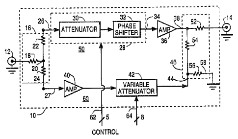
FIGURE 7. is a simplified diagram in block and
schematic form of a predistortion equalizer adapted for
operation at microwave or millimeter-wave (RF) operating
frequencies. In FIGURE l, predistortion equalizer 10
includes an input port 12 and an output port 14. Input
port 12 is adapted to receive signal from a source (not
illustrated) which is to be predistorted by
6/'~ ; . < ; ~> r' s)
~~7 J i:J .s
-6- 80AE2909
predistortion equalizer 10, and port 14 is adapted to be
coupled to an amplifier arrangement (not illustrated)
which is operated at a level such that amplitude
distortion tends to occur. Such an amplifier might be a
travelling-wave tube amplifier or paralleled solid-state
amplifier array. Of course, the amplifier arrangement
may include final power amplifiers and separate
preamplifiers, as appropriate.
Signals to be amplified applied to input port
12 from the source are applied to a first end of a
resistor 18, the other end of which is connected to a
node 20. One end of each of resistors 22 and 24 are
also connected to node 20. Resistors 18, 22 and 24
together form a resistive signal amplitude or power
divider illustrated as 16, which accepts signals from
input port 12, divides the signal into two
equal-amplitude portions, and applies those portions
over conductors illustrated as 26 and 27 to the input
terminals (not separately designated) of an upper
channel 50 and a lower channel 60, respectively. The
signals on conductors 26 and 27, in addition to being of
equal amplitude, are of equal phase. For purposes of
differentiating between "ports" and "terminals" herein,
the term °'port'° connotes an impedance match to a desired
characteristic, while "terminals°' do not necessarily
suggest such an impedance match.
Upper channel 50 is intended to be a linear
reference channel and lower channel 60 is intended to be
a nonlinear channel. Those skilled in the art know that
linearity if a matter of degree, and that upper channel
50 may have nonlinearities.
Upper channel 50 includes a phase shifter
illustrated .in dotts:d outline 28. The input of phase
shifter 28 is connected to conductor 26 for receiving an
input signal from resistive divider 16, far producing a
phase-shifted signal on a conductor 34. Phase shifter
28 is controlled by five-bit control signals applied
~a '.; ;.a ,~.. ,; ~" a
--7-- 80AE2909
over a data bus &2 from a control source (not
illustrated). Phase shifter 28 is inherently lossy,
having a nominal loss of about 8 d~, which may vary
depending upon the cantrol signal configuration or logic
state. The separate functional aspects of phase shifter
28 are illustrated by the cascade of an attenuator block
30 and a phase shifter block 32 within the outline of
phase shifter 28. Phase shifter 28 produces
phase-shifted and attenuated signals on a conductor 34
l0 for application to an amplifier 35. Amplifier 36 has
sufficient output power capability to produce a
substantially linear signal on a conductor 38 within its
operating input levels.
Lower channel 50 includes an amplifier 40, the
input of which is coupled to conductor 27 for receiving
a portion of the divided signal from resistive power
divider 16. The output of amplifier 40 is coupled to a
controllable or variable attenuator illustrated as a
block 42, which is controlled by six-bit control signals
applied over a data bus 64 from a control source (not
illustrated). Amplifier 40 has an amplitude distortion
which changes as a function of the signal level applied
to its input terminal. Typically, such a distortion
manifests itself as a compression at higher signal
levels. As is known to those skilled in the art, such
compression may be stated in terms of a percent of
compression or, in the case of a multichannel input
signal, may be stated in terms of a
carrier-to-intermodulation distortion. It should
particularly be noted that amplifiers 36 and 40 may be
similar amplifiers operated at similar bias levels,
whereby the difference in linearity or distortion is
attributable to the larger input signal applied to the
input of amplifier 40 by comparison with that applied ~to
amplifier 36. The amplified signal produced by
amplifier 40 is applied by way of variable attenuator 42
to an input terminal 44 of a resistive signal combiner
rA ~i f ~J .i,'.. ~ ' ~ n ~ i
-8- 80A~2909
46. Similarly, the output of amplifier 46 is applied to
input terminal 38 of signal combiner 46,
Resistive signal combiner 46 includes a first
resistor 52 connected between its input terminal 38 and
output port 14. A second resistor 54 has one end
connected to input terminal 38, and the other end to
input terminal 44. A third resistor 56 is connected
between input terminal 44 and a source of reference
potential such as ground 58. Resistive combiner 46
combines the relatively nonlinear signal applied to
input terminal 44 with the relatively linear signal
applied to input terminal 38. Phase shifter 32 is
adjusted to create a relative phase shift between the
linear and nonlinear signals applied to resistive
combiner 46, which phase shift lies within the range of
90° and 270°, and which for ease of understanding may be
considered to have a nominal value of 180°, representing
an out-phase condition.
The signal voltage appearing at the output of
amplifier 369 at the output of the top or upper channel
50 can be represented as
VT = Vin ~ AT ~ GT LBT + Bd (1)
caheres
Vin is the voltage level applied to power
divider 16;
AT is the attenuation ratio of power divider
16 together with the inherent attenuation of top or
upper channel phase shifter 28, as represented by ideal
attenuatar 30;
GT is the gain of top channel amplifier 36;
BT is the inherent phase shift of the top
channel other than that introduced by ideal phase
shifter 32; and
e~ :~%; ' %'
-9-- 80AE2909
Bd is the phase shift introduced by ideal
phase shifter 32 and controlled by the control signal
applied over bus 62.
Similarly, the s:i.gnal voltage VB appearing at
the output of bottom ar lower channel 60 can be
represented as
VB = Vin ~ GB ~ AB LBB (2)
where:
Vin is the voltage level applied to power
divider 16 from input port 12~
GB is the gain of bottom channel amplifier 40;
AB is the attenuation ratio of power divider
16 together with that of bottom channel attenuator 42t
and
BB is the inherent phase shift introduced by
the bottom channel.
Resistive output signal combiner 46 combines
signal VT received at its input terminal 38 with signal
VB received at its input terminal 44 to produce an
output signal voltage V~u~ at output port 14
Vout - Van (AT~GTLBT+Bd + GB~ABLBB) (3)
Assuming that the inherent phase shifts of the
top and bottom channels are the same, or may be
compensated by an additional phase shift introduced by
phase shifter 32 so as to be the same, and further
assuming that the functional phase shift introduced by
phase shifter 32 is ~r or 180°, then
Vout ° Vin (AT~GT~~GB~AB) (4)
and the gain of the predistortion equalizer becomes
G
~V d '. ~ ~.i ;.1
-10- 80AE2909
GAIN - Vout
(AT~GT-GB~AB) (5)
V.
m
Since the top path is assumed to be always
linear, the product AT~GT remains constant for all input
signal levels. The product GB~AB, however, decreases in
magnitude with increasing magnitude of Vin, as amplifier
40 is driven toward saturation. With increasing input
signal level, therefore, progressively less signal is
subtracted from AT~GT, and the combined signal at output
port 14 has an expanding transfer function or
characteristic. An expanding transfer function is the
opposite of a compression, and may be useful for
predistortion correction.
For values of Bd ranging from about 90° to
270°, an expanding transfer function characteristic also
occurs, but accompanied by an associated change in
phase. If Bd is in the range of 90° to 180°, the phase
shift of the output signal increases as a function of
input level, while for Bd in the range of 180° to about
270°, the phase shift of the output signal decreases
with increasing signal level. By appropriate selection
of phase shift Bd and the attenuation of attenuator 42,
almost any combination of expansion and phase shift may
be generated. Naturally, if the increments provided by
5-bit phase shift and 6-bit attenuation are too coarse,
a greater number of bits may be used, or analog phase.
shifters or attenuators may be used.
A major advantage of the embodiment of FTGURE
1 lies in the use of resistive signal power divider 16
and resistive signal power combiner 46 instead of by the
use of inductively coupled transformers or
inductively-~oapacitively coupled circuits such as
directional couplers, which tend to change their
coupling factors and phase at frequencies other than the
center frequency of the design band. While such changes
in coupling factor arid phase are small, the differences
,v . ., .2 r,J : i
~..> in .'_ ''<.7 ..:r .',r
-11- 80AE2909
are magnified or exacerbated due to the fact that signal
subtraction, or 'the difference between the signals in
the channels, is used for the output signal.
Ideally, the structure illustrated in FIGURE 1
is formed as a monolithic microwave integrated circuit
(MIMIC) in order to maximize bandwidth and to fully take
advantage of the bandwidth improvements provided by the
use of resistive dividers and combiners. In a
particular embodiment of the invention, resistors 18, 22
and 24 of resistive dividers 16 each have a resistance
value of 16.6 ohms, and resistors 52, 54 and 56 of
resistive combiner 46 have resistance values of 15, 100
and 68 ohms, respectively. Five-bit digital phase
shifter 28 has an inherent attenuation of 8 dB and phase
increments of about 5° per step. Six-bit variable
attenuator 42 has a range of about a-3 to -30 dB, and
amplifiers 36 and 40 each have a gain in the range of 6
to 8 dB over a frequency range 11.2 to 11.7 GHz,
centered on 11.5 GHz.
FIGURE 2a illustrates as a plot 200 the gain
of linear upper channel 50 as a function of the phase
shifter logic state at a frequency of 11.95 Ghz, and
plot 202 illustrates the corresponding phase in degrees.
FIGURE 2b illustrates as a plot 204 the output power in
dBm plotted against the input power in dBm for the
linear upper channel for a phase shifter logic state of
10000, corresponding roughly to 180° of phase shift.
plot 206 is a corresponding plot for a control code
logic state of 00010. The value 10000 corresponds to
maximum attenuation of the phase shifter, as can be
verified by referring to FIGURE 2a. The plot 206
represents a lower loss condition of phase shifter 28 of
FIGURE 1 than plot 104, and as a result the upper
channel has higher gain. As can be seen by comparison
of plots 104 and 106, little compression results at
higher input power levels.
i~o'~yl~.. ~,~,~n
-12- a0AE2909
Plat 300 of FIGURE 3a illustrates the gain of
lower channel 60 of FIGURE 1 at 11.95 GHz as a function
of the logic state of the control code applied over data
bus 64 to attenuator 42 of FIGURE 1. The gain is
maximum (attenuation is least) for codes greater than
about 110000. Correspondingly, gain is minimum
(attenuation is maximum) for codes near 000000. Plot
302 illustrates the phase in degrees resulting from
attenuation control. Plot 304 of FIGURE 3b illustrates
l0 the output power in dBm relative to input power in dBm
for the lower channel 60 of FIGURE 1 at a frequency of
11.95 GHz for a logic state of 111100 (minimum
attenuation) of the control code applied to variable
attenuator 42 of FIGURE 1. Plot 304 substantially
correspands to minimum attenuation, and therefore plot
304 represents the maximum gain. The magnitude of the
gain may be determined by noting the difference between
the input power and the output power for any point on
the curve. For example, an input power of -10 dBm
provides an output power of about -5 dBm, thereby
indicating a gain of 5 dB. Compression or deviation
away from a gain of about 5 dB accurs at an input power
of about -4 dBm. Plot 306 of FIGURE 3b is a
corresponding p7.ot for a control input logic state of
000000 (maximum attenuation). With maximum signal
attenuation of attenuator 42, at an input power of
-10 dBm, output power is about -12 dBm, indicating a
gain of -2 dB. Thus, control of attenuator 42 between
codes 000000 and 111100 can result in a gain change of
lower channel 60 of FIGURE 1 of about 7 dB. The onset
of compression continues to occur at about -4 dBm of
input signal power.
FIGUREB 4a, 4b and 4c illustrate plots of
magnitude and phase of the transfer function of the
arrangement of FIGURE 1 between parts 12 and 14 at 11.95
GHz for various control conditions. In FIGURE 4a, plot
400 represents the magnitude and plot 402 the phase for
d ~~..o ~! , . . .e
-13- 80AE2909
a phase shifter control signal of 000111 and an
attenuator control signal of 010000. Plot 400
represents a gain expansion o:E 0.9 dB and a phase lag
over the illustrated range of +3°. In FIGURE 4b, plot
404 represents the magnitude and plot 406 the phase.
For a phase shifter control logic state of 00011 and an
attenuator logic state of 010000. This provides a gain
expansion of 0.9 dB and a phase lead of 3° across the
illustrated range of input signals. In FIGURE 4c, plot
408 illustrates the magnitude and plot 410 illustrates
the phase across a range of input signal levels with a
phase shifter control logic state of 00110 and an
attenuator logic state of 110000. The plots of FIGURE
4c represent a gain expansion of 1..5 d8 and a phase lead
of 13° across the illustrated range of input signal
levels.
In FIGURE 5, plots 502, 505 and 507 are made
at 11.2, 11.5 and 11.7 GHz, respectively, and represent
the carrier-to-intermodulation (C/I) distortion in d8
occurring at those three frequencies for various amounts
of backoff from maximum power level of a combination of
the predistortion equalizer of FIGURE 1 and a particular
following power amplifier. At maximum output power,
corresponding to low values of backoff, the distortion
is in the range of 16 to 20 dB below the desired signal
carrier level. As backoff increases to about 10 dB, the
distortion decreases in a roughly monotonic manner to
the range of 32 to 40 dB. The three plots 502, 505 and
507 are approximately parallel, indicating that at all
frequencies in the frequency range of interest the
change in distortion level as a function of backoff is
predictable. Plot 510 of FIGURE 5 represents the best
of the results at one of 11.2, 11.5 and 11.7 GHz for a
prior art diode linearizer utilizing hybrid couplers.
Plot 510 is not monotonic, and does not achieve as good
a result as the arrangement of the invention for certain
frequencies and backoff levels.
., , ,
~l ,.n ~ , .~ " ..f
-14- 80A~290~
Other embodiments of the invention will be
apparent to those skilled in the art. The values of the
resistors used in resistive dividers and combiners
according to the invention will depend upon the
characteristic impedances of the ports to which they are
intended to be coupled, arid upon~the power division.
For example, top channel 50 may be made more linear and
bottom channel 60 more nonlinear by increasing the
resistance of resistor 22 by comparison with that of
resistor 24. Similarly, resistive combiner 45 presents
attenuation between its input port 44 and its input port
48, which may be traded against the resistance of
variable attenuator 42.
While the resistive power combiner nominally
introduces no phase shift, it is asymmetrical as to the
two signal paths and therefore actually introduces some
residual phase shift, which is not considered
significant in view of the phase shift linearity errors
in the controllable attenuator and phase shifter. The
distortion errors manifest themselves in many ways, and
the exact nature of the distortion manifestation is not
considered important, as for example in some
multichannel television application the distortion
manifestation known as °°cross-modulation" may be more
important than either intermodulation distortion or
compression. Connection ports have been described as
impedance-matched, but those skilled in the art know
that such "matches" are ideal, and in practice are
subject to wide variations ordinarily known or specified
by VSWR, return loss, or S11.