Note: Descriptions are shown in the official language in which they were submitted.
~, 202T
INFORMATION RECORDING AND REPRODUCING DEVICE
The present invention relates to an i~rulll " ~ recording and
reproducing device for recording and reproducing i"' Illdliol, on and from
various types of memory devices such as a magneto-optical disk, wherein
pieces of i"' Illd~iOll such as address ;llr " " ~ are ~l~dt,l~llllill~ly
5 recorded, and more , ~ relates to timing control of i,,rul,,,dliol, recording
and reproduction.
On a magneto-optical disk, a thin magnetic film having vertical
magnetic al ,: ~. u~,y is usually used as a recording medium, and a laser beam -which is focused to a spot of sub:~ldl ,' 'Iy 1,um - is applied thereto in order to
1û perform recording, reproducing and erasing ope,dLiui,s. More Lr- ~ 'Iy, the
recording and erasing ope,.~t;o"~ are achieved by effecting a Illa~ dliUIl
reversal with an external magnetic field by utilizing the fact that the coerciveforce required is lowered because of a l~ Ire rise at the location where
the laser beam is focused. On the other hand, the reproducing operation is
15 achieved by utilizing the fact that the plane of p~ldl- " ~ of a laser beam
rotates due to a magneto-optical effect, and by s~hseq~ently detecting the
rotation of the polarizing plane by an analyzer.
An dlldl~9~:lllelll is provided wherein each track of the magneto-
optical disk is divided into a plurality of sectors in the circu",' ~IIlidl direction,
20 and in the leading area of each sector, a pre-format part is disposed. In the pre-format part, a sector mark, address i"~ ",dlion and other data are
plt:d_lt:llllill ' ~y formed in pits, while recording, reproducing and erasing
o~ldliol,s of magneto-optical signals are performed in the other area of each
sector - as a recording area for magneto-optical signals by each sector unit. In25 such case, it is necessary to provide timing control so that recording,
reproducing and erasing up~ldliol~s can be performed for magneto-optical
signals in the recording area (excluding the pre-format part).
In a conventional illfUlllldLiùl~ recording and reproducing device a
reproduced signal is output from an illfUlllldliul~ reproducing circuit, and the30 reproduced signal is input to a sy~ul~ulli~dlioll detection circuit. In the
*
F
2~
sy"ul"u"i~dliù" detection circuit, sy.,~l,,u,,i~dliu,~ detection for each sector is
pe,rul,,,ad from, for example, a signal of a sector mark which is a part of the
reproduced signal.
A sy".,I " u, Ii~dliull detection signal produced by the s~"~cl~, u,,
5 detection circuit is input to a timing control circuit, where timing control is
provided according to the syr,~,l,,u,,i~dliull detection signal. Consequently, areproducing timing signal is sent to the i~ru~ dLiull reproducing circuit during a
reprûducing operation, while a recording/erasing timing signal is sent to an
i"' Illdliull recording/erasing circuit during a recording or erasing operation.10 With this alldil~c~ ll, recording, reproducing and erasing o,ce, 'i~ ~s are
perfommed in the recording area for magneto-optical signals of each sector.
'' .,.~I'y, the sy"~l"u,ii~dliull detection by the s~.~ulllull ~ detection
circuit is performed separately from the reproducing operation of il,fulllldlioll so
as not to disturb the syllulllulli~dlioll detection due to the reproducing timing
1 5 signal.
However, in the prior art device, since the timing control is
provided only by the use of the syll11llulli~dliùli detection, there OCCd~iOI~ 'ly
arise cases wherein an error occurs in s~llul~lulli~dliu~ detection or a time lag
in detection occurs in the sy,,cl,,u,,i~dliùl~ detection circuit. Consequently,
20 accurate timing control cannot be executed. More ;~ y~ errors in the
timing control arise because read gate signals of a PLL (Phase-Locked Loop)
included in the i"' " IdliUI i reproducing circuit become inaccurate, consequently
pulling-in ope,dliu"s cannot be performed, and runout of the locked loop is apt
to occur. Accordingly, the conventional method has a problem in that the
25 reliability of the recording, reproducing and erasing ~ IdliUl~s cannot be fully
achieved . Further, when an error occurs in 3JI ,~,I " u, li~dliUIl detection, the timing
control of the AGC (Automatic Gain Control) is adversely affected.
It is an object of the present invention to provide timing control for
accurate recording and reproducing U~ Idt~Olis without time lag if an error
30 should occur in the sy,)~,l"u"i,dliu" detection signals.
~,
3 202 1 6 8 1
The invention is an i,,ru,,,,dliul~ recording and reproducing device
which performs an i"rul Illdliùl~ recording erasing and reproducing operation onor from a memory device having pre-format sections each including a sector
mark section formed therein. The device comprises i" ",..t;o" reproducing
5 means i" " Id~iUi, recording/erasing means sectortiming detection means and
timing control means. The sector timing detection means produces a sector
timing detection signal based on a sector mark signal reproduced by the
i~ru~ dLiull reproducing means from the sector mark sections. The il~fulllldl
reproducing means reproduces an analog signal according to a reproducing
10 timing signal released from the timing control means. The i"'~r",dliu,~
reproducing means reproduces the sector mark signal from the sector mark
sections and prûduces a pre-recorded area detection signal based on the
detected Le:llllilldLioll of the pre-format sections. The i" IlldLi
recording/erasing means performs an i,,.'u,,,,dLiùn recording and erasing
15 operation according to a recording/erasing timing signal from the timing control
means. The timing control means produces the reproducing timing signal and
the ,~co,di"g~rasing timing signal based on the sector mark signal except
during those times when the sector timing detection signal is judged to be in
error at which times the timing signals are based instead on the pre-recorded
20 area detection signal.
The i"~.", . l reproducing means may comprise a waveform
shaping circuit and a pre-recorded area detection circuit. The shaping circuit
shapes a waveform of the reproduced analog signal to convert that signal to a
binary-coded reproduced digital signal. The detection circuit releases the pre-
25 recorded area detection signal for a ~ d~'~.",i"ed period of time followingoutput of pulses from the waveform shaping circuit thereby permitting detection
of the pre-format section as the pre-recorded area. The pre-recorded
j~ ~C~ ~ ~ IdLiol ' area detection circuit may comprise a re-ll iyg~l dL~I~ pulse y~ LiUll
circuit formed by a re-LIiyg~ldL,k: Illu~G~LdL,l~ multivibrator provided with
30 resistors and capacitors for d~ llllillilly a time constant or by a shift register.
The re-L~iyyt:,dl,le pulse y~ ldtioll circuit may comprise a divider and an AND
.~
4 2o2l68;
circuit. The divider has a clear input terminal, a clock input terminal and an
output terminal, the reproduced digital signal being entered thereinto through th~
clear input terminal thereof. The AND circuit has one of its input terminals
cu"ne-,led to the output terminal of the divider, and the other of its input
5 terminals co""e,,le:.l to a reference clock signal for a dividing operation, and its
output c~""e~ d to the clock input signal.
The illru~ d~ioll reproducing means may comprise a pre-format
waveform p~oces5;~19 section, a recording signal waveform prucessi"g section,
a data ~ lllvl,i,dlion section, and a signal ,ulu~,eaailIg control section. The
10 pre-format waveform ~, uCl~:aSil 19 section releases a first reproduced digital signal
co, lt~ i"g to the pre-format section, and generates the sector mark signal.
The recording signal wavefomm prucessi"g section releases a second
reproduced digital signal co~ ,o~ to a recorded signal. The data
s~"~l"~"i~dlion section has a PLL circuit whereby the section releases
15 Sy~ l"u"uus data sy"~,l"u"i~i"g to a reference clock, according to the first and
second reproduced digital signals from the respective waveform ~,ucessi"g
sections. The signal plùc~:,si,lg control section has a pre-recorded area
detection circuit for permitting the pre-recorded area detection circuit to release
a pre-recorded area detection signal and for releasing timing signals for each
20 of the sections. Either the first reproduced digital signal or the second
reproduced digital signal is released to the data s~ ul~i~dliOI~ section
according to the timing signals.
The sector timing detection means may include a sector mark
detection circuit, a counter, a timer circuit, a window ~ e,dliull circuit, a
25 judgement circuit, a switching circuit, and a recording signal section judgement
circuit. The sector mark detection circuit releases a sector mark detection
signal according to the sector mark signal. The counter releases a negative
pulse signal after having reached a ~,~d~,.",i"ed count number following a
falling edge of the sector mark detection signal. The timer circuit releases a
30 negative pulse signal after having reached a count number cO"~::,pOI,~ 9 to
one sector portion in addition to the count number by the counter. The window
~,
5 20216~T
9e~ 1dtiOI~ circuit releases a negative pulse signal having a ,.,~d~ "i"ed
window width in the vicinity of a falling edge of the next sector mark detectionsignal based on a falling edge of a preceding sector mark detection signal. The
judgement circuit releases a binary timing judgement signal of a "High" level
5 when a falling edge of the sector mark detection signal is detected during a
negative-pulse period of the output of the window gellelaliol~ circuit and
releases the signal of a "Low" level when a falling edge of the sector mark
detection signal is not detected during the same condition. The switching circuit
selects an output of the counter as a reference timing signal when the timing
10 judgement signal is in the "High" level and selects an output of the timer circuit
as the same when the timing judgement signal is in the "Low" level. The
recording signal section judgement circuit releases a first recording signal
section judgement signal as negative pulse signal during a period co" t:~pon.lil ,9
to a recorded section within one sector according to the reference timing signal.
15 The reference timing signal timing judgement signal and recording signal
section judgement signal are thereby permitted to be sent to the timing control
means.
The sector mark detection circult may include a plurality of
counters for succes~ively counting count numbers and releasing the results as
20 a detecting signal. Each count number is directly plO~o,liu"àl to each length of
marks and non-marks according to the sector mark signal. The sector mark
detection circuit also includes a judgement circuit for judging whether the
detecting signal coincides with each ~,~d~ ""i"ed length of marks and non-
marks in the sector mark section and whether the order thereof is properly
25 followed.
The timing control means may comprise a first counter a second
counter and a switching circuit. The first counter releases a positive pulse by
counting a period during which the pre-recorded area detection signal is in the
"High" level and by regarding it as reproducing a pre-format section if the
3û period continues for not less than a l,,t:d~r,,,i,,ed period. The second counter
starts a counting operation sy"-l"u"i~i"g to a rising edge of the positive pulse
D ~
6 202,68l
of the first counter, and releases a second recording signal section judgement
signal which falls to a "Low" level in the vicinity of a border between a pre-
fommat section and a recording signal section, and rises to a "High" level in the
vicinity of the next border between a recording signal section and a pre-format
5 section. The switching signal i"' .~,I,dll~eably switches the second recording signal section judgement signal of the second counter to the first recording
signal section judgement signal of the recording signal section judgement circuit,
and releases it as a reproduction timing signal.
The switching circuit may comprise a D-type flip-flop, a first
10 inverter, a second inverter, and first and second NAND circuits. The D-type flip-
flop includes a data input terminal, a clock input terminal, a positive phase
output terminal and a negative phase output terminal, and has the timing
judgement signal entered into the data input temminal thereof. The first inverter
reverses a polarity of the first recording signal section judgement signal, and
15 releases it to the clock input terminal of the D-type flip-flop. The second inverter
reverses a polarity of a signal released from the positive phase output terminalof the D-type flip-flop. The first NAND circuit receives a signal from the negative
phase output terminal of the D-type flip-flop and the second recording signal
section judgement signal. The second NAND circuit receives the outputs of the
20 second inverter and the first NAND circuit, for executing NAND ~,pe,dliu,~:, and
for releasing the reproduction timing signal. With this dllally~llle:nl, the first
recording signal section judgement signal is released as the reproduction timingsignal when the signal from the positive phase output terminal of the D-type flip-
flop is in a "High" level, and the second recording signal section judgement
25 signal is released as the reproduction timing signal when the signal from thepositive phase output terminal of the D-type flip-flop is in a "Low" level.
The pre-recorded area detection circuit may further include a
leading pulse removing circuit for nullifying an output of the re-l, i~ge, dble pulse
~neldlioll circuit with respect to a ~ dt:l~"";"e~ number of leading pulses in
30 the reproduced digital signal, thereby permitting the pre-recorded area detection
signal to be detected accurately even if there is contained at least one defect
E
7 20 2 1 6 8 1
pulse in the reproduced digital signal. The leading pulse removing circuit may
comprise a modulo-N counter for nullifying the output of the re-l, iyy~l dbl~ pulse
gellt:ld~ivil circuit with respect to leading pulses the number of which is given
by N in the reproduced digital signal. The leading pulse removing circuit may
5 ~ " " ":~IJ be a shift register.
The pre-recorded area detection circuit may further include a shift
register having a clear input terminal, a clock input temminal, a data input
terminal and an output terminal, and having an output of the re-t, iyye, dl,le pulse
gt:,~e,..'iol, circuit entered into the clear input terminal thereof, the reproduced
digital signal entered into the clock input terminal thereof, and high levels of the
reproduced signal constantly entered into the data input terminal thereof. This
dl I dl lyt~ permits the pre-recorded area detedion signal to be released from
the output temminal.
The invention will be more readily u"de,~tuod from the following
des.,,i~,t~J,~ of preferred e",L,o~i",~"l~ with reference to the accu"")d"ying
drawings, in which:
Figure 1 (a) to (d) are time charts showing a gel ,~, ' ,9 sequence
of pre-recorded area detecting signals;
Figure 2 is a schematic plan view showing a magneto-optical disk;
Figure 3 is an enlarged partial view of Figure 2;
Figure 4 is a block diagram showing an i"' Illdlioll recording and
reproducing device;
Figure 5 is a block diagram showing an i"ru"" ' ~ reproducing
circuit;
Figures 6 to 8 are ~ ldll ' -y diagrams lu~pe-,ti~cly showing
examples of a re-L,igge,d~le pulse gell~ldlioll circuit;
Figure 9 is a block diagram showing a detailed dlldll9ellle:11l of an
i"' Illdliull reproducing circuit;
Figure 10 is a block diagram showing a detailed dlldlly~:",el,l of
30 a _J. ,~,l ll u" ' , detection circuit;
E
2o2l68l
Figure 11 is a block diagram showing a detailed a"ai,g~",~"l of
a sector mark detection circuit;
Figure 1 2(a) to (e) are ~:~plal laluly diagrams showing the operation
of a counter circuit;
Figure 13 is a time chart showing the progress of each signal in
the ~ 1llUIli~d~iOl~ detection circuit;
Figure 14 is a block diagram showing a detailed a"d"ge",~"~ of
a timing control circuit;
Figure 15 is a time chart showing the progress of each signal in
1û the timing control circuit;
Figure 16 is a circuit diagram showing a detailed configuration of
a switching circuit;
Figure 17 is a time chart showing the progress of each signal in
the switching circuit;
Figures 18 to 2û illustrate an alternate ~",~û~i",e"l of the present
invention;
Figure 18 is a block diagram showing an i"ru"" ' 1 reproducing
circuit;
Figures 19 and 2û are t:.~,ulal laluly diagrams showing examples of
a pre-recorded area detection circuit; and
Figure 21 is a block diagram showing a conventional i"r~", "
recording and reproducing device.
Figure 21 illustrates a conventional illrUlllldliùl~ recording and
reproducing device for p~, ru" "i"g recording and reproducing u,u~, dLiOI ,S on and
from a magneto-optical disk by the use of the above-",~l,liol1ed method. A
reproduced signal A is outputfrom an i,,ru,,,,dliol~ reproducing circuit 1, and the
reproduced signal A is input to a Sy.,-.l"u~ ali~l, detection circuit 2. In the
syl~11llulliLaliull detectiûn circuit 2, sy"ul"u"iLaliùl~ detection for each sector is
pe,rur,,,~d from, for example, a signal of a sector mark which is a part of the
reproduced signal A.
.~
202 ~ 68 1
A s~"-,l"u"i~liol) detection signal B produced by the
sy"..l"u"i~dliul1 detection circuit 2 is input to a timing control circuit 3, where
timing control is provided according to the syllul"u"i~dliul1 detection signal B.
Consequently, a reproducing timing signal C is sent to the illrUlllldlio
5 reproducing circuit 1 during a reproducing operation, while a recording/erasing
timing signal E is sent to an i"'~ recording/erasing circuit 4 during a
recording or erasing operation. Vvith this d"di1g~",~"l, recording, reproducing
and erasing U,U~ldliùl~s are performed in the recording area for magneto-opticalsignals of each sector. ~ , the sy"ul"ul,i,dliùll detection by the
0 sy"ul 11 u~ dliOIl detection circuit 2 is performed S~pdl ' Iy from the reproducing
operation of i"' r" " , so as not to disturb the Sy.,~;l"u"i~dliu~l detection due
to the reproducing timing signal C.
However, in the device shown in Figure 21, since the timing control
is provided only by the use of the syn.,l"o, ,i~dliùn detection, there OCl,dsiul, 'Iy
15 arise cases wherein an error occurs in ~,llulll~ dliull detection, or a time lag
in detection occurs in the sy", I~u~ 11 detection circuit 2. Consequently, an
accurate timing control cannot be executed. More -r '~ 'Iy. errors in the
timing control arise because read gate signals of a PLL (Phase-Locked Loop)
included in the i~r~ dliùl1 reproducing circuit 1 become inaccurate,
20 consequently pulling-in Op~ liù11s cannot be pe,ru""ed, and runout of the
locked loop is apt to occur. Accordingly, the conventional method has a
problem in that the reliability of the recording, reproducing and erasing
o~, " 1S cannot be fully achieved. Further, when an error occurs in
sy,)cl,,u,,i~i~lioll detection, the timing control of the AGC (Automatic Gain
25 Control) is adversely affected.
The following d~s~,,i,", will discuss one ~",~o~i",er,l of the
present invention with reference to Figures 1 to 17.
In Figure 2, there is shown a magneto-optical disk 10 as an
example of an optical memory device on/from which recording, reproducing or
30 erasing up~,i " ,:, are executed by an i"ru"" " ~ recording and reproducing
device according to the present invention. On the magneto-optical disk 10,
,~
202 ~ 68 1
there are provided tracks 11 in a spiral shape, or in a cul~ct:ll k. shape, and
each track 11 is divided into a plurality of sectors 12 in the CirC~ rt~ idl
direction. A pre-format section 13 is disposed in a leading area of each sector
12, and the remaining area thereof forms a magneto-optical signal section 14.
As shown in Figure 3, in the pre-format section 13, there are
pl~:d~ "i,l ' ~y recorded a plurality of marks 15 (shown in hatching for
convenience) fommed in pits, and non-marks which are space sections between
those marks 15. In the magneto-optical signal section 14, there are recorded
a plurality of marks 16 (shown in hatching for convenience) formed by magneto-
optical signals, and non-marks which are space sections between those marks
16. The marks 15 are ~ " ";, IdL~Iy formed physically, and therefore are not
erasable; however, the marks 16 are l~colddl; 1~ as well as erasable.
Additionally, either each mark 15, 16, or each non-mark located in between,
cvllt:~Jol~ds to a signal "1"; the remaining area c~ olld~ to a signal "0".
Figure 13(a) shows a sector format, which is a format of each
sector 12. The pre-format section 13 includes a sector mark section 13a, for
s~ ,l"v"i~i"~ each of the sectors 12, and an ID section 13b having address
i"" ", " ~ of the sectors 12.
The magneto-optical signal section 14 includes a data section 14a,
for recording magneto-optical signals therein, and gap sections 14b, 14c.
Basically, data is recorded in the data section 14a by using marks 16 and non-
marks provided by magneto-optical signals. The gap sections 14b, 14c are
margin sections for allowing a recording start position and a recording end
position to be dislocated forward or backward by phase errors which occur when
sy"~;l"v"i~i"g each of the sectors 12 to the rotation of a spindle motor which
rotates the magneto-optical disk 10.
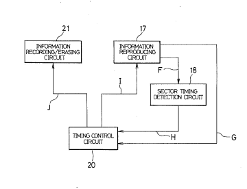
As shown in Figure 4, the i,,ru,,,,dtiv~ recording and reproducing
device of the present invention comprises an illru,,,,dliul~ reproducing circuit 17
(illrv~ d~iOI~ reproducing means). From the i"' r",~ reproducing circuit 17,
reproducing signals including a sector mark signal F are sent to a sector timingdetection circuit 18, as will be described later.
.,
11 202~681
Furthermore, from the il~full~ldliul~ reproducing circuit 17, a pre-
recorded area detecting signal G (which will be described in detail later) is sent
to a timing control circuit 2û as a timing control means. A sylu,lllu,l " )
detection signal H, which will be described in detail later, generated in the sector
5 timing detection circuit 18 according to the sector mark signal F is also sent to
the timing control circuit 20. Based on those signals, a reproduction timing
signal I is released from the timing control circuit 20 to the illru,,,,dli
reproducing circuit 17, and a recording/erasing timing signal J is released to an
ldli~ COI~ ,,d~ l9 circuit 21.
As shown in Figure 5, the il~ru~ dliol) reproducing circuit 17
comprises a pre-recorded area detection circuit 24 including a waveform
shaping circuit 22 and a re-l,i~g~,d~le pulse gel)erdliu,, circuit 23. Circuit 17 is
designed to detect the pre-format sections 13 as a pre-recorded area having a
sector mark recorded therein.
More -r ~ r~ an analog signal K (see Figure 1(a)) reproduced
from the pre-format section 13 of the magneto-optical disk 10 is entered into the
waveform shaping circuit 22, where it is converted to a reproduced digital signal
L (see Figure 1(b)) as a binary-coded digital signal of "High" or "Low". The
reproduced digital signal L is entered to the pre-recorded area detection circuit
20 24. When a pulse exists in the reproduced digital signal L, the pre-recorded
area detection circuit 24 turns the pre-recorded area detecting signal G (see (c)
in Figure 1) to "High" and keeps it in that state for T seconds. Since the pre-
recorded area detection circuit 24 includes the re-lliy~eldble pulse yent:,dliul)
circuit 23, when the next pulse is entered within the r seconds after the
25 preceding pulse was entered in the reproduced digital signal L, the pre-recorded
area detecting signal G is kept "High" for the S~'C^,f ~ " ,g T seconds.
One example of an d,ldi~g~",er,l of the re-l,i~e,dule pulse
gel)t:ldliul) circuit 23 is shown in Figure 6. Here, the re-l,iygeldbl~ pulse
9~",:, ) circuit 23 includes a re-ll iy~l dUI~ " lollo~ldblt: multivibrator 25. The
3û period of time T for keeping the pre-recorded area detecting signal G high is
;
~,
12 2021 681
pr~d~t~ ",i"dl~:ly set by a resistor R and a capacitor C wherein T is directly
plUp~lliOlldl to the product R.C.
Figure 7 shows another example of an a"~i,gt:",~"L of the re-
l~iyge,d~l~ pulse ~ llW ~ circuit 23, wherein a shift register 26 is employed.
5 Serial input to an input terminal IN is given as "High" and clock pulses having
a frequency fc are entered to a clock terminal CK; then a N-th output of a shiftoutput terminal QN is released as a pre-recorded area detecting signal G.
Further a reproduced digital signal L is entered to a clear terminal CL. In thatcase the equation is ~ sed as: T = N x (1 / fc)
1û Figure 8 shows another example of an dlldl1gl:lllC~ of the re-
11 igge, dul~: pulse gel ,~, ~ circuit 23 wherein a modulo-N divider 27 is
employed. The reproduced digital signal L is entered to a clear terminal CL,
and an output of an output terminal OUT is released as a pre-recorded area
detecting signal G. The pre-recorded area detecting signal G is entered to one
of the input temminals of an AND circuit 28. Further clock pulses having a
frequency fc are entered to the other of the input terminals of the AND circuit 28
and an output signal of the AND circuit 28 is entered to a clock terminal CK of
the modulo-N divider 27. In that case the equation is similarly ~x~ ssed as:
r=Nx(1 /fc).
2û Shown in Figure 1 (a) to (c) are a group of pulses derived from the
marks 15 formed in pits in a reproduced analog signal K from the pre-format
section 13 on the magneto-optical disk 10. The group of pulses are converted
in the waveform shaping circult 22 to binary-coded signals which form a
reproduced digital signal L. As a method for converting them to binary-coded
signals amplitude detection peak detection or other method is used. When a
pulse in the reproduced digital signal L is entered into the pre-recorded area
detection circuit 24 the period of time T for which the pre-recorded area
detecting signal G stays "High" is ,.,~d~.l"i" Iy set so as to be more than
a maximum pulse period Tma,~ in the group of pulses in the reproduced digital
signal L. As a result the pre-recorded area detecting signal G as an output
signal of the pre-recorded area detection circuit 24 has a form shown in Figure
-
~r'
13 202 1 68 1
1(c) forming a signal having a portion thereof s~b~ld~ ly equal to that
produced in the pre-format section 13 by the group of pulses in the reproduced
analog signal K.
The following d~s. ,iulioll will discuss a detailed example of an
dlldllyelllC~ of the il~fUlllldLiOIl reproducing circuit 17 referring to Figure 9.
The reproduced analog signal K reproduced from the magneto-
optical disk 10 is entered into a buffer amplifier 30 in the i"'~ Illdlioll
reproducing circuit 17. A reproduced analog signal K amplified by the buffer
amplifier 30 is entered into both a magneto-optical signal waveform u, uces ~ y
1û section 31 and a pre-format waveform plucessi"g section 32. The magneto-
optical signal waveform ~,ucessi"g section 31 and the pre-format waveform
pru~es:,i"g section 32 are respectively designed based on the dru,t:",e:"~ ed
waveform shaping circuit 22 (see Figure 5). From the magneto-optical signal
waveform prucessi"g section 31 and the pre-format waveform p~ uces:.i"9 circuit
32 are l,::,ueuli-cly released reproduced digital signals L1 and L2 as binary-
coded signals. Those signals c~ ,uulld to marks 16 15 and non-marks in
between in the respective magneto-optical signal section 14 and pre-format
section 13.
The reproduced digital signals L1 L2 are entered to a data
sy~cl,,u,,i~dliùll section 33 where according to a PLL (Phase-Locked Loop)
therein synchronous data M syl~- l " u, ,i~t:d to clock pulses is released and sent
to a demodulation circuit which is not shown in the figures. Also a sector mark
signal F is generated according to the sector mark section 1 3a in the pre-format
waveform p,uces~i"g section 32 and is sent to the sector timing dekction
circuit 18 (see Figure 4).
A signal u,uces;,i"g control section 34 is designed to release
various control and timing signals N O P Q to the buffer amplifier 3û
magneto-optical signal waveform pluces~ g section 31 pre-format waveform
r,,~essi"g section 32 and data s~,n.l,,ulli,dliull section 33 respectively.
Moreover the signal p, uces .;~ ,g control section 34 includes therein
the ~ liuned pre-recorded area detection circuit 24 (see Figure 5) and
.,
14 202 1 68 1
is designed to release the pre-recorded area detecting signal G according to thereproduced digital signals L from the data sy".il llulli~dliol~ section 33. Further
a reproduction timing signal I is entered into the signal ~uces~ g control
section 34.
The following dt:s~ will next discuss a detailed example of
an ~" ~"gt:" ,e"l of the sector timing detection circuit 18 referring to Figures 10
to 17. In Figure 10 the sector mark signal F released from the i" r",
reproducing circuit 17 is entered into a sector mark detection circuit 35 in thesector timing detection circuit 18. Detection of the sector mark section 1 3a ispe,ru""ed in the sector mark detection circuit 35.
More :",e~ iri. ~l J as shown in Figure 11, the sector mark detection
circuit 35 comprises a counter circuit 36 having counters No. 1 to No. 9 and a
judgement circuit 37. The sector mark signal F released from the i~C~r~ lio
reproducing circuit 17 is entered to counters No. 1 to No. 9. Output signals V1
to V9 of those counters No. 1 to No. 9 are respectively entered to the judgementcircuit 37 and according to those signals a sector mark detecting signal R is
released from the judgement circuit 37.
Figure 12 is a diagram describing the operation of the counters No.
1 to No. 9. As shown in Figure 12(b) there are recorded marks 15 (shown in
hatching for convenience) and non-marks located in between in the sector
mark section 13a as t:",t:" led. In this example as shown in Figure
12(a) the marks 15 are physically provided so that a ratio of the mark lengths
to the non-mark lengths can be t~ ssed as 5:3:3:7:3:3:3:3:5. The sector
mark signal F (Figure 12(c)) obtained by the pattern of those marks and non-
marks 1ulli :,pond~ to for example "0" in the mark 15 and "1" in the non-mark.
When the reproduced signal of these marks 15 and non-marks is entered to the
counters No. 1 to No. 9 firstly a mark length of the leading mark 15 is counted
by the counter No. 1 as shown in Figure 12(e). When the counted number
(Figure 12(d)) is within a p,t:d~t~ ",i"ed range co"~:".u"di"g to a mark length
"5" the detection of the leading mark 15 is confirmed. Secondly in the counter
No. 2 the s~ cc~ - ,g non-mark having a non-mark length "3" is detected in the
2021 681
same procedure. Then, the marks 15 and non-marks in the sector mark section
1 3a are successively detected by the counters No. 3 to No. 8, and lastly the last
mark 15 having a mark length "5" is detected by the counter No. 9.
Detecting signals V1 to V9 for those nine marks 15 and non-marks
5 are entered to the judgment circuit 37. Then, it is judged whether those nine
results of the detection conform to the pattern of the sector mark section 13a,
and whether an order of each of those marks 15 and non-marks is properly
followed. Consequently, only in the case where the length of each of those
marks 15 and non-marks as well as the order thereof is apprupli ' does the
10 sector mark detecting signal R becomes "Low", thereby showing that a sector
mark has been detected.
As shown in Figure 10, the sector mark detecting signal R is
entered to a counter 38, a timer circuit 40 and a judgement circuit 41
,ueuli/cly. Output signals S and T of the counter 38 and the timer circuit 40
15 ~ ,ueu~i/cly are entered to a switching circuit 42, where one of the signals is
selected according to a timing judgement signal H2 from the judgement circuit
41 which will be described later, and is released as a reference timing signal U.
The reference timing signal U is entered to a magneto-optical signal judgement
circuit 43 (recording signal section judgement circuit), and a first magneto-
20 optical signal section judgement signal H1 (recording signal section judgementsignal) is released, as will be described in detail h~leilldr~l.
From the timer circuit 40, an output signal W is also entered to a
window ~ e,dliu" circuit 44 (which will be described in detail later). An outputsignal X from the window ~ el ' ~ circuit 44 is entered to the judgement
25 circuit 41. In the judgement circuit 41, according to the output signal X and the
sector mark detecting signal R from the sector mark detection circuit 35, the
timing judgement signal H2 is released, as will be described h~ illd~l, and
sent to the switching circuit 42 and the timing control circuit 20.
According to the reference timing signal U, the first magneto-
30 optical signal section judgement signal H1 and the timing judgement signal H2,
16 202 1 68 1
a recording/erasing timing signal J and a reproduction timing signal 1 which areshown in Figure 4 are released from the timing control circuit 20.
Figure 13 shows a waveform of each of those signals shown in
Figure 10. The sector mark detecting signal R (Figure 13(b)) becomes "Low"
when a sector mark section 13a of the pre-format section 13 is detected. A
falling edge of the sector mark detecting signal R provides timing for
s""~l"uni~;"g the sector 12. The counter 38 shown in Figure 1û changes its
output signal S (Figure 13(c)) to "Low" upon reaching the p,~d~'~.",i"ed count
after the receipt of the rising edge.
On the other hand the timer circuit 40 is u,~d~'~r",i"dl~ly set to
have the count number for one sector and has that count number in addition
to the count number by the counter 38. Accordingly a falling edge of an output
signal T (Figure 1 3(d)) of the timer circuit 40 is Sl~b~ al 1' 'Iy sy, lul ll u~ d with
the falling edge of the output signal S of the counter 38 in the next sector 12. Moreover based on the falling edge of the sector mark detecting
signal R an output signal X (Figure 1 3(e)) of the window ~ erd~iul1 circuit 44
is ~ d~ "i, ~y set to become "Low" with a ~l~d~te~ ,ed window width in
the vicinity of a falling edge of the sector mark detecting signal R in the nextsector 12.
The timing judgement signal H2 (Figure 13(f)) released from the
judgement circuit 41 is u, ~dt:lel " ,i, Idl~:ly set so that it may become "High" in the
presence of a falling edge of the sector mark detecting signal R when the outputsignal X of the window ~:"e,dliun circuit 44 is "Low"; on the other hand signal
H2 may become "Low" in the absence of a falling edge of the sector mark
detecting signal R when the output signal X of the window gel1e, aliul1 circuit 44
is "Low". Accordingly the timing judgement signal H2 functions as a signal for
judging whether the detection of a sector mark section 13a is executed within
a ,~ d~r",i"ed range.
In the switching circuit 42 shown in Figure 10 the output signal S
of the counter 38 is selected when a sector mark section 1 3a is detected; on the
other hand the output signals T of the timer circuit 40 is selected if a sector
17 202 ~ 68 1
mark section 13a is not detected. Accordingly, the reference timing signal U
(Figure 13(9)) properly provides timing control for detecting a sector mark
section 13a according to the output signal T from the timer circuit 40, even if an
error occurs in detecting a sector mark section 13a.
The magneto-optical signal judgement circuit 43, to which the
reference timing signal U is entered, is a type of counter, and the first magneto-
optical signal section judgement signal H 1 thereof (Figure 1 3(h)) becomes "Low"
during the magneto-optical signal section 14. In other words, the first magneto-optical signal section judgement signal H1 is a signal for judging between the
magneto-optical signal section 14 and the pre-fommat section 13. The
dru~ ,ed reference timing signal U, timing judgement signal H2 and f rst
magneto-optical signal section judgement signal H1 are sent to the timing
control circuit 20.
The following des~,,i, " ~ will next discuss a detailed example of
an d"dl~ge",~"l of the timing control circuit 20. In Figure 14, the pre-recordedarea detecting signal G is entered to a first counter 45 in the timing control
circuit 20. An output signal Y of the first counter 45 is entered to a second
counter 46. An output signal of the second counter 46 becomes "Low" during
the magneto-optical signal section 14, as will be described later, and the signal
forms a second magneto-optical signal section judgement signal M (a second
recording signal section judgement signal). The second magneto-optical signal
section judgement signal AA is entered to a switching circuit 47.
Into the switching circuit 47 the first magneto-optical signal section
judgement signal H1 and the timing judgement signal H2 are also entered, as
Sy"-,l"u"i~dliu" detection signals H. According to the timing judgement signal
H2, the first magneto-optical signal section judgement signal H1 and the second
magneto-optical signal section judgement signal AA are illL~I~,lldllgedbly
switched to form the reproduction timing signal 1, which is released therefrom
to be entered into the ill~)lllld~iUIl reproducing circuit 17.
As shown in Figure 15(b), the pre-recorded area detecting signal
G to be entered to the f rst counter 45 becomes "High" during the pre-format
18 202 1 68 1
section 13, as dru,~",~"liuned according to Figure 1; the rising edge is
sub~ldll 'Iy sy~,~,l"u"i~t:d with the start position of the pre-format section 13.
It is p, t:d~l~l " ,;" Iy designed that when the pre-recorded area detecting signal
G has been successively "High" for not less than a ~,~.le,l~""i"ed byte length
5 (for example, seventeen bytes), the output signal Y of the first counter 45
changes from "Low" to "High", as shown in Figure 1 5(c). In other words, in the
first counter 45, judgement of whether it is a pre-format section 13 or not is
made according to a byte length of the pre-recorded area detecting signal G.
Based on a rising edge of the output signal Y of the first counter
45, the second counter 46 is operated as shown in Figure 15(d). Further, it is
p~d~ 'y set that the second magneto-optical signal section judgement
signal M as an output signal from the second counter 46 changes from "High"
to "Low" in the vicinity of a border between a pre-format section 13 and a
magneto-optical signal section 14 (for example, at the gap section 14b in Figure15(a)). It is also ~ d~ ly set that the second magneto-optical signal
section judgement signal AA returns from "Low" to "High" again in the vicinlty
of the next border between the magneto-optical signal section 14 and a pre-
format section 13 (for example, at the gap section 14c in the Figure 15(a)).
Therefore, the second magneto-optical signal section judgement signal M
functions as a timing signal which is formed according to the pre-recorded area
detecting signal G.
al'J, in the timing control circuit 20, ",oll~aldl;l~
multivibrators may be, ~ ,eut;~cly used instead of the first and second counters45, 46.
A detailed example of an dlldllg~ of the switching circuit 47
is shown in Figure 16. The first magneto-optical signal section judgement signal(first recording signal section judgement signal) H1 as the S~rllCl~lul~i~dliol~detection signal H is entered to a clock input terminal CK of a flip-flop 50 (which
is, for example, a 74LS74 integrated chip of U.S. Texas Instrument Co., Ltd.)
through an inverter 48 (first inverter) in the switching circult 47. On the other
hand, the timing judgement signal H2, as it is, is entered to a data input terminal
_
19 202 1 68 1
D of the flip-flop 50. An output signal BB from an output terminal Q (positive
phase output terminal) is entered to both terminals of a NAND circuit 51 (secondinverter), while an output signal CC of an output terminal Q (negative phase
output terminal) is entered to one of the input terminals of a NAND circuit 52
(first NAND circuit). Furthermore, the second magneto-optical signal section
judgement signal (second recording signal section judgement signal) AA is
entered to the other of the input terminals of the NAND circuit 52. Output
signals DD, EE from the ~,ueu~iic NAND circuits 51, 52 are entered to a NAND
circuit 53 (second NAND circuit), and an output signal of the NAND circuit 53
forms the reproduction timing signal 1.
Figure 17 shows waveforms of the respective signals in Figure 16.
The first magneto-optical signal section judgement signal H1 (Figure 17(c)) and
the second magneto-optical signal section judgement signal M (Figure 17(e))
become "Low" during a magneto-optical section 14 (see Figure 17(a)). Upon
receiving the timing judgement signal H2 (Figure 17(b)) at a falling edge of thefirst magneto-optical signal section judgement signal H1, the output signal BB
(Figure 17(d)) from the output terminal Q of the flip-flop 50 is obtained. When
the output signal BB is "High" as shown by a solid line, detection of a sector
mark section 13a is executed normally; however, when it is "Low" as shown by
a dotted line, occurrence of an error is confirmed. Further, the circuit shown in
Figure 16 is designed so that the first magneto-optical signal section judgementsignal H1 is released as the reproduction timing signal I when the output signalBB from the output terminal Q of the flip-flop 50 is "High", while the second
magneto-optical signal section judgement signal AA is released as the
reproduction timing signal I when the output signal BB is "Low". Accordingly,
even if an error occurs in detecting sector mark sections 13a, timing control may
be cu"",al~sdLt:d based on the pre-recorded area detecting signal G.
The reproduction timing signal I provides, for example, the
following control op~ s.
First, the reproduction timing signal I can be used for switching an
input signal to the PLL of the data sy,)~.l"u" " , section 33 shown in Figure
2 0 2 1 68 1
9. More :"., ~ 'Iy, in the case of using the magneto-optical disk 10, as shown
in Figure 2, it is necessary to properly switch between the reproduced signals
L1 and L2 before their entry to the PLL in the data s~"~,l"u, " n section 33.
Thatisnecessarybecausethe~ _~/ufur,,,a~ el,Li,,gthemarks15andmarks
16 in the reproduced analog signals K' are S~Udl ' ~y prucessed in the
It:apeuti/c pre-format waveform pluc~ssi"g section 32 and magneto-optical
signal waveform p~uces~ g section 31.
Secondly, the reproduction timing signal I can be used for judging
whether signals of the magneto-optical signal section 14 are demodulated, or
those of address illru""dliol, of the pre-format section 13 are demodulated, in
a demodulating operation of a demodulation circuit, (which is not shown in the
figures) installed as a step after the data syllulllu"i~dliol, section 33.
Lastly, in the case of an error occurring in reproduction, it is
necessary to detect it and release the il,~ Illdliu11 about it. Therefore, the
reproduction timing signal I is used for judging whether the error in reproduction
has occurred in the magneto-optical signal section 14 or has occurred in the
pre-format section 13. In all three of these examples, the reproduction timing
signal I is used for judging whether the signals are from the magneto-optical
signal section 14 or from the pre-format section 13.
The pre-recorded area detecting signal G not only c~",~.e,):.dl~s
the timing control which operates by detecting the sector mark section 13a
within the pre-format section 13, but is also utilized in the following cases.
More ir ~ 'I~, the signal can be used as a read gate signal for
the PLL in the data Sy.,-,l"u"i~dliul~ section 33. Further, in order to provide
timing control for AGC (Automatic Gain Control), the signal is used for turning
on the AGC only in the areas having data recorded, and for holding it in the
other areas. Furthermore, the signal is used for detecting burst errors of
recording signals. In all three above examples, the pre-recorded area detecting
signal G is used for judging whether an area has illrUlllldliUll recorded therein
or not, in the magneto-optical signal section 14 or in the pre-format section 13.
Accordingly, the pre-recorded area detecting signal G, which is used in the
E
21 202 1 68 1
above cases, is applicable not only to the pre-fommat section 13 which is the
pre-recorded section but also to the magneto-optical signal section 14 wherein
illru~ dliOII recording, reproducing and erasing U,Ut:ldliOI~s are pe,ru""ad.
The following des-,li, " ~ will discuss the second e",Lo~i",e"~ of
the present invention, referring to Figures 18 to 20.
The second ~" l~o~i" ,e"~ deals with the case where a defect pulse,
such as shown by a dotted line s or in Figure 1(a), occurs at a section other
than the pre-format section 13 in the magneto-optical disk 10. It provides
proper measures to prevent occurrence of an error in illfUlllld~iull reproduction
due to malfunctions where the pre-recorded area detecting signal G becomes
"High" erroneously because of a defect pulse - as shown by a dotted line u or
_ in Figure 1(c).
More -r~ '' 'Iy, the pre-recorded area detection circuit 24
included in the illru,,,,d~iul~ reproducing circuit 17 co",,u,ises a re-~,iyye,~le
pulse gel1~, , circuit 54 and a leading pulse removing circuit 55, as shown
in Figure 18. The leading pulse removing circuit 55 functions as a circuit for
nullifying the output of the re-~,iyg~ pulse ~elleldLiol1 circuit 54 for one or
more leading pulses, the number of which is given by integer M in the
reproduced digital signal L.
A concrete example of an dlldll9t:111elll of the leading pulse
removing circuit 55 is shown in Figure 19. Here, a modulo-M counter 56 is
disposed as the leading pulse removing circuit 55 in a step before the re-
11 i~yel dblt: pulse yt:i 'e, , circuit 54. The modulo-M counter 56 removes the
leading pulses (the number of which is given by integer M) from the reproduced
digital signal L. Additionally, instead of the modulo-M counter 56, a M-shift
register may be used.
Figure 2û shows another example of the d"d"y~",a"l of the
leading pulse removing circuit 55, where a shift register 57 is disposed as the
leading pulse removing circuit 55 at a step after the re-l,iy~e:,d~le pulse
g~ne, , circuit 54. An output of the pulse g~:~)e~d~iul1 circuit 54 is entered to
a clear terminal CL of the shift register 57, while the reproduced digital signal
22 202~681
L is entered to a clock terminal CK of the shift register 57, thereby releasing an
M-th shifted output QM as a pre-recorded detecting signal G'.
The following des-,": ~ will discuss, for example, timing control
in a situation where M = 1, that is to say, the output of the re-l, iyge:l dLI~ pulse
5 gel1erdliùll circu-lt 55 is nullified for only one leading pulse of the reproduced
digital signal L.
As shown in Figure 1 (a), if there is only one defect pulse within an
un-recorded area of i"' l l l " ), the defect pulse is nullified by the leading pulse
removing circuit 55. Figure 1(d) shows the pre-recorded area detecting signal
10 G' becoming "High" due to a defect pulse not being nullified.
Moreover, in the pre-format section 13, the timing of the pre-
recorded area detecting signal G' going "High" is delayed by only one pulse;
however, read gate timing for the PLL, for example, is not affected by the delayof a few pulses. Thus, the reliability of the PLL is not adversely affected.
In the above ~::IIIUOIIillle:lll, i~rUI IlldliOIl recording, reproducing and
erasing o~e, ,:, are performed on and from the magneto-optical disk 10;
however, the present invention is applicable to other devices for use in
reproducing from various optical memory devices, or to those of DRAW (Direct
Read After Write)-type constitution. Further, the present invention is 1,~, ' ' '
20 to i"e~r",dliol1 recording and reproducing devices wherein magnetic memory
devices have a grouping of illfullll ~ pulses for indicating those areas which
have been recorded, as well as to those devices wherein optical memory
devices are used.
As e~ ~",e" ~ed, the i,,f~r,,,dliun recording and reproducing
25 device of the present invention, which records and reproduces i"ru", 1 on
and from an optical memory device, comprises a pre-recorded area detection
circuit for detecting a pre-recorded area having i"ru""..'~ol, ul~d~l~llllilldl~ly
recorded and located on the memory device. It also comprises timing control
means for providing timing control of an jlle~ Illdliùl~ recording or reproducing
30 operation according to a pre-recorded area detecting signal released from thepre-recorded area detection circuit. With this ~"di,g~",el,l, since the timing
23 2021 681
control of the i"~ ldliull recording, reproducing and erasing ope,dLi~l,s is
provided according to the pre-recorded area detecting signal, timing of
recording, reproducing, or erasing operation is accurately d~ta,l"i"ed.
Additionally, the timing control may be performed according to both the pre-
5 recorded area detecting signal of the present invention and the conventionalsy,,~;l,,u,, " 1 detection signal. In that case, if an error should occur in the
s~"cl"ul, " 1 detection signal, since the pre-recorded area detecting signal
isreleasedeverytimepre-recordedil~fu,,,,dLiu,~forasectormarkisreproduced,
an accurate timing control without time lag is achieved according to the pre-
1û recorded area detecting signals.
The invention being thus described, it may be obvious that the
same may be varied in many ways. Such variations are not to be regarded as
a departure from the scope of the invention.