Note: Descriptions are shown in the official language in which they were submitted.
2~21~88
P~ASE: 15ATCHING CIRC~IIT
.. BACI~GROUND OF ~HB INVBN~ION
a. Field of the Invention
The present invention relates to a phase matching circuit
. for receiving first data synchronized with a first clock and
outputting second data of the same content as the first data
synchronized with a second clock which has the same frequency as
the first clock, and more particularly to a phase matching
circuit suitable for chanqing the clock from the receiving clock
to a system clock at a terminal repeater in a synchronous
multiplex transmission system for transmitting a signal having
used and unused data regions.
b. Description of the ~elated Art -
In an apparatus for high speed transmission of signals which
multiplex a voice signal and an image signal, the transmitter and
receiver are operated synchronously. In this case, a phase
matching circuit is provided within a terminal repeater
connecting respective units in order to match the phase of the
clocks of the respective units for the purpose of changing the
clocks in the adequate timing during transfer of clocks between
the units. However, although the prior art includes such a phase
matching circuit, it has generated a problem in that accurate
processing cannot be carried out in the receiving apparatus
because valid data which are read in the receiving side apparatus
~ ' .:
f . .- . .
2~216~8
2- 25307-247
are missed or such valid data are read twice due to the matching of
the clocks using the phase matching circuit associated with the
prior art.
BRI~F DESCRIPTION OF THE DRAWINGS
Fig. 1 is a block diagram illustrating a phase matching
circuit of the prior art;
Figs. 2A-2F and Figs. 3A-3F are timing charts illustrating
the operation of Fig. l;
Fig. 4 is a block diagram illustrating the basic principal
of the present invention;
Fig. 5 is a block diagram illustrating a first em~odiment
of the phase matching circuit of the present invention;
Fig. 6 is a block diagram illustrating a second embodiment
of the phase matching circuit of the present invention; and
Fig. 7A-7G and Fig. 8A-8G are timing charts illustrating
the operation of the phase matching circuit of the present
invention.
These together with other objects and advantaqes which will
be subsequently apparent, reside in the details of construction and
operation as more fully hereinafter described and claimed, refer-
ence being had to the accompanying drawings forming a part hereof,wherein like numerals refer to like parts throughout.
An example of the structure of a known phase matching
circuit is shown in Fig. 1. CKl denotes a first clock used in the
transmitting side apparatus, while Dl denotes first data output
from the transmitting side apparatus. CK2 denotes a second clock
2~21~8
-2a- 25307-247
used in the receiving side apparatus, while D2 denotes second data
input to the receiving side apparatus. The first data Dl and
second data D2 have the same content, and the first clock and
second clock have the same frequency.
. Reference numeral 101 denotes an input buffer which takes
the first data Dl from the transmitting apparatus in accordance
with the first clock CKl used in the transmitting apparatus, 102
denotes an output buffer which sends the second data D2 of the
r same content as the first data Dl to the receiving apparatus in
accordance with the seeond clock CK2 used in the reeeiving appara-
tus, 103 denotes a phase deteetor whieh inputs and eompares the :
phases of the first clock CKl and the seeond clock CK2 and deter-
mines whether the phase differenee between the two clocks is within
a predetermined value, and 104 denotes a phase controller which
eontrols the timing for punehing the first data Dl whieh is input
in aeeordanee with the seeond eloek CK2 either direetly or inverted
based on the deteetion result of the phase deteetor 103. -
2~2~68~
.
,.
In the phase matching circuit shown in Fig. 1, th~ first
data D1 is taken by the first clock CXl from the transmitting
apparatus. The phase detector 103 receives the first clock CKl
and the second clock CK2 and detects whether a phase difference
- 5 is within the predetermined value or not. Detection of the phase
difference is necessary because if the first clock CKl and the
t second clock CK2 have the same phase, then there is a high
probability that when data is taken the content of receiving data
will be changing in the receiving apparatus. Thus, accurate data
lo reading is not possible. Therefore, when two clocks come close
to the same phase, this problem occurs. This problem has been
solved by shifting the phase of the first data D1 with a phase
matching circuit.
The phase controller 104, which consists of an intermediate
buffer 105 and a clock switch 106, receives the second clock CK2
and either inverts the second clock CK2 or uses it directly,
depending on whether the phase difference between the first clock
CKl and the second clock CK2 is within the predetermined value or ;
not. That is, the clock switch 106 causes data to be read from
the intermediate buffer 105 with a clock, which is either the
second clock CK2 directly or the second clock CK2 inverted
depending on the phase difference detected by the phase detector
103. Whe,n the second clock CK2 is inverted due to such phase
shift control, the inverted second clock is thereafter inverted
again or normalized to the second clock CK2 when the phase
difference is no longer within the predetermined value. As a
3--
- 2~2~8-
result, phase shift control is carried out for the data being
transmitted. However, the phase matching circuit associated with
the prior art discussed above results in the following problems.
Figs. 2A-2F and Figs. 3A-3F illustrate timing charts for the
phase matching circuit associated with the prior art.
Designations A-F shown in Fig. 1 correspond to the timing charts
of Figs. 2A-2F and of Figs. 3A-3F, respectively. Figs. 2A-2F
indicate that when the phase detector 103 detects the phase
difference to be within the predetermined value, the phase of the
second clock CK2 is shifted by inverting the second clock CK2 in
the clock switch 106. Figs. 3A-3F indicate that when the phase
difference exceeds the predetermined value after being within the
predetermined value, the inverted second clock is inverted again
or normalized to the normal phase of the second clock CK2 in the
clock switch 106. These phase shift operations cause the phase
of the data to shift. A problem of such phase shift control,
however, is that data are missed or read twice, as shown in Figs.
2F and 3F. That is, the phase matching circuit associated with
the prior art carries out phase shift control without relation to
the content of the data. As a result, the above-mentioned
problem arises in that the valid data to be read in the receiving
side is missed or read twice. Thus, accurate processing cannot
be conducted in the receiving side.
~ 2~21~88
-5- 25307-247
SUMMARY OF THE INVENTION
. It is therefore an object of the present invention to
'; provide a phase matching circuit which realizes accurate data trans-
. mission and reception by performing phase shift control only during
t, a valid region of the data. The resulting improved phase shift
.j~ circuit utilizes the fact that the data includes a valid regionwhich is read in the receiving apparatus and an invalid region
, which is not read in the receiving apparatus.
According to the aspect, the present invention provides a
phase matching system for converting first data from a transmission
' 10 system to second data for a reception system, the first data is .
synchronized with a first clock having a first phase and the second
', data is synchronized with a second clock having a second phase, the
first data has used and unused data regions, said phase matching :;:
system comprising: phase comparison means for comparing a phase
difference between the first phase of the first clock and the :~
second phase of the second clock with a predetermined value to
produce a phase difference signal; data detection means for detect- .
ingone of the used and unused data regions of the first data; phase
shift control means for converting the se¢ond clock into an inter-
mediate clock, for inverting the intermediate clock to produce an -
inverted intermediate clock when the phase difference signal in-
dicates the phase difference is less than the predetermined value
and when said data detection means detects one of the unused data
regions, and for outputting the first data in accordance with one
i': ', ' ' ', ''. . , . ', : ~,:: ' ,, . , . "' . ', ' ' . ' . ' :
2~21g~
-5a- 25307-247
of the intermediate clock when the inverted intermediate clock is
: not produced and the inverted intermediate clock when the inverted
intermediate clock is produced.
According to another aspect, the present invention provides
a phase matching circuit for converting first data synchronized
with a first clock into second data, the second data having the
same content as the first data and synchronized with ~he second
clock having the same fre~uency as the first clock, said phase
recelv~ng
matching circuit comprising: input buffer means for ta~g the
first data with the ~4ca~ clock, the first data includes used and
unused data regions; output buffer means for sending the second
data with the second clock; phase detector means for comparing
phases of the first and second clocks to detect a phase difference
within a predetermined value; phase control means, operatively ~.
connected to said input buffer means, said output buffer means and
said phase detector means, for performing phase shift control by one
of outputting directly the first data to said output buffer means
when the phase difference within the predetermined value is not
detected by said phase detector means, and outputting the first
data phase shifted to said output buffer means when the phase
difference within the predetermined value is detected by said phase
detector means; unused data region detector means for detecting one
of the unused data regions within the first data; and phase shift
controller means, operatively connected to said unused data region -
detector means, for inhibiting the phase shift control by said
phase control means when said unused data region detector means does : -
2 ~ 2 ~ ~ 8 g
-5b- 25307-247
not detect one of the unused data regions and for allowing the
phase shift control in said phase control means when said unused
data region detector means detects one of the unused data regions.
According to yet annother aspect, the present invention
provides a method for converting first data from a transmission
system to second data for a reception system, the first data is
synchronized with a first clock having a first phase and the
second data is synchronized with a second clock having a second
phase, the first data has used and unused data regions, said method
comprising the steps of:
(a) receiving the first data, the first clock and the second
clock;
(b) determining a phase difference between the first phase of
the first clock and the second phase of the second clock;
(c) comparing the phase difference with a predetermined value;
(d) producing a phase difference signal based on said comparing
in step (c);
(e) detecting one of the used and unused data regions in the
first data
(f) shifting the first data to produce shifted first data
when the phase difference signal indicates the phase difference is
less than the predetermined value and when said detecting in step . -
(e) detects one of the unused data regions; and :
(h) outputting one of the first data and the shifted first
data as the second data.
,
,:,
.
2 Q 2 5 ~ ~ 8
-5c- 25307-247
~ ccordl.ng to a further aspect, the present lnvention
provides a me~l~od for converting first da~a from a transmisslon
sy~tem to second data ~or a reception system, the fir~t data is
synchronized witll a firs~ clock having a ~irst phase and tlle
second data is synchroni~ed wlth a ~econd clock having a second
phase, the first data has used and unused data regions, said method
comprislng the steps of:
(a) receiving the first data, the flrst clock and the second
clock
(b1 determining a pha~e difference between the flrst phase of
the first clock and the second pha~e oE the second clock
(c) comparing the phase difference Witil a predetermined value;
(d) produclng a phase difference signal based on sald comparing
in step (c);
(e) detecting one of the used and unused data regions ln the
first data;
(f) converting the second clock lnto an intermediate clock
(g) invertlng the intermediate clock to produce an inverted
lntermedlate clock when the phase difference signal indlcates the : :
phase dlEference 1~ less than the predetermined value and when sald
detecing in step (e) detects one of the unused data reglons ~ :
~ h) producing lntermediate data from the first data in
accordance wlth one of the intermediate clock when the inverted
intermediate clock is not produced and the inverted intermediate :-
clock when the lnverted intermedlate clock is produced in step
2~2~8
` -6- 25307-247
: (g);
- (i) outputting the second data from the intermediate data in
accordance with the second clock.
DESCRIPTION OF THE PREFERRED EMBODIMENTS
The basic principal of the invention together with pre-
ferred embodiments of the present invention will be explained in
detail
. ~.
',~ "
.
:
2~2~8
below with reference to Figs. 4-7.
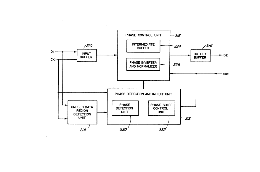
The basic principle of the present invention is illustrated
in Fig. 4. The present invention relates to phase matching
circuit formed by an input buffer 210, a phase detection and
` 5 inhibit unit 212, an unused data region and detection unit 214, aphase control unit 216, and an output buffer 218. The input
buffer 210 receives input data as first data Dl and an input
clock as a first clock CK1 from a transmitting apparatus. The
first clock CKl is sent to the phase detection and inhibit unit
lo 212 and the unused data region detection unit 214. The output
buffer 218 sends out output data as second data D2 to a receiving
apparatus using a second clock CK2 provided by the receiving
apparatus. The second clock CK2 is sent to the phase detection
and inhibit unit 212 and the phase control unit 216.
Next, the phase detection and inhibit unit 212 compares the
phase of the first clock CKl with the phase of the second clock
CK2 to determine if the phase difference is within a ~-
predetermined value. This operation is performed by a phase
detection unit 220 which i8 included within the phase detection
and inhibit unit 212. Meanwhile, the unused data region
detection unit 214 determines whether the first data Dl is in an
unused data region (invalid region) or an used data region (valid
region). Then, the phase detection and inhibit unit 212 produces
a phase inversion signal based upon the phase difference detected
by the phase detection unit 220 and the detection of data regions
by the unused data region detection unit 214.
....
-7-
.
2~21~8
.
More particularly, when the phase detection unit 220 detects
` the phase difference within the predetermined value the phase
inversion signal is produced. However, the phase inversion
signal is not output to the phase control unit 216 until an
.
unused data region is detected by the unused data region
detection unit 214. This gating or inhibiting operation is
performed by a phase shift control unit 222 contained within the
phase detection and inhibit unit 212.
Once the phase inversion signal is output from the phase
detection and inhibit unit 212, the phase control unit 216
controls the phase shift operation. The phase control unit 216
includes an intermediate buffer 224 and a phase inverter and
normalizer 226. The phase inverter and normalizer 226 receives
the phase inver6ion signal and shifts or inverts the second clock
CK2 when the phase inversion signal indicates that the phase
difference is within the predetermined value. The phase inverter
and nor~alizer 226 outputs an intermediate clock which
corresponds to either the second clock CK2 directly or the second
clock after having been shifted or inverted. The intermediate
buffer 224 then receives the first data Dl in accordance with the
intermediate clock, thus causing a shift in phase of the first
data. Finally, the first data, whether shifted or not, is output
by the output buffer 218.
Fig. 5 illustrates a first embodiment of the present
invention. The first embodiment will be explained in detail with
regard to Fig. 5.
--8--
' .~ -
~2~
The phase matching circuit of the first embodiment is formed
by an input buffer 310, an unused data region detector 314, a
phase controller 316, an output buffer 313, a phase detector 320,
and a phase shift controller 322. The input buffer 310 receives
the input data as the first data D1 and the input clock as the
first clock CKl, and is formed by a D-type flip-flop. The output
buffer 318 receives the second clock CX2 and outputs the output
data as the second data D2, and is also formed by a D-type flip-
flop. The output data has the same content as the input data,
and the output clock has the same frequency as the input clock.
Although invalid data may be lost or read twice, the consequence
of such is harmless to the correct reception of the valid data.
The phase detector 320 detects whether the second clock CK2
has a phase difference from the phase of first clock CKl that is
within the predetermined value or not. The phase detector 320
can also be formed by a D-type flip-flop. The first clock CKl is
input to the data input ~D input) and the second clock CK2 is
input to the clock input (C input) of the D-type flip-flop 320.
Therefore, the output of the D-type flip-flop 320 becomes "1"
when the phase difference between the first clock CKl and the
second clock CK2 is within the predetermined value. In all other
cases, the output of the D-type flip-flop 320 becomes "0".
The phase controller 316 applies the first data Dl either
directly or phase shifted to the output buffer 2 depending on the
result of the detecting by the phase detector 320. Therefore, -~
the phase controller 316 includes a phase inverter and normalizer
_g
-` ~02~
, . . .
'''
326 which inverts or normalizes the second clock CK2 depending on
the result of the detecting by the phase detector 320. The phase
inverter and normalizer 326 corresponds to the clock switch 106
. described above. The phase controller 316 also includes an
intermediate buffer 324 and a delay circuit 328 The
.,~ .
intermediate buffer 324 receives data output from the input
buffer 310 and applies such data to the output buffer 318. As
the intermediate buffer 41, a D-type flip-flop can be used like
the input buffer 310 and output buffer 318.
The delay circuit 328 is provided to delay the second clock
. CK2 so that data can be accurately read in the intermediate
buffer 324. The delay circuit 328 delays the second clock CK2
prior to its input to the phase inverter and normalizer 326.
Note, however, that alternatively the delay circuit 328 could be
located at the clock input (C input) of the output buffer 318.
That is, the delay circuit 328 is provided so that the clock
input to the intermediate buffer 324 and the clock input to the -~
output buffer 318 are not in phase.
The phase inverter and normalizer 326 inverts the second
clock CK2 when the phase detector 320 detects a phase difference
within the predetermined value between the first clock CKl and
the second clock CK2. Alternatively, the phase inverter and
normalizer 326 outputs the second clock CK2 in its normal phase
when the phase detector 320 detects a phase difference greater :
than the predetermined value between the first clock CKl and the
second clock CK2. As the phase inverter and normalizer 326, an
--10-- :
r~
$ 8
exclusive OR gate (EXOR gate) can be used.
The unused data region detector 314 can also be formed by a
-type flip-flop. The unused data region detector 314 detects
an unused data region using identification data contained in the
first data Dl. The identification data i8, for example, binary
data which is "1" for a used data region or "O" for an unused
data region. The data input (D input) of D-type ~lip-flop 314
receives the identification data and the first clock CKl is input
to the clock input (C input) as shown in Fig. 5. The
identification data is a signal which exists, for example, in the
header of each frame of the first data Dl to indicate whether or
not the data in the frame includes data to be read and used in
the receiving apparatus. The circuit diagram of the first
embodiment shown in Fig. 5 indicates an apparatus for processing
only one bit in order to simplify the explanation. `
~ The phase shift controller 322 inhibits phase shift control
in the phase controller 316, even when a phase difference within
the predetermined value is detected by the phase detector 320,
until the unused data region detector 314 detects an unused data
region in the first data Dl. That is, the phase shift controller
322 allows phase shift control in the phase controller 324 only
when the unused data region is detected and not when a used data --
region i8 detected. A D-type flip-flop can be used as the phase
shift controller 322. The output from the phase detector 320 is
input to the data input (D input) of D-type flip-flop forming the ~
phase shift controller 322 and the output fxom the unused data -
~ .:
--1 1--
2~2~
region detector 314 is input to the clock input (C input)
thereof.
The result detected by the phase detector 320 i8 maintained
in the phase shift controller 322 until an unused data region is
detected by the unused data region detector 314. Once an unused
data region is detected, the data maintained is then applied to
the phase inverter and normalizer 326 of the phase controller
316. When the unused data region detector 314 detects an unused
data region, it causes the phase shift controller 322 to latch
the output from the phase detector 320. Namely, the phase shift
controller 322 is inserted between the phase detector 320 and the
phase controller 316 so that the data input to the phase :
controller 316 is not altered until the unused data region is
detected.
With the structure mentioned above, the first data Dl is
applied to the output buffer 318 either directly or phase shifted
depending on the detection result of the phase detector 320.
However, if the unused data region detector 314 does not detect
the unused data reqion of the input data Dl, phase shift control
in the phase shift controller 316 is inhibited by holding the
detection result previously output from the phase detector 320 in
the phase shift controller 322. Thereafter, phase shift control
i5 allowed by latching the detection result currently output from
the phase detector 320 when the unused data region detector 314
detects an unused data region of the first data Dl.
'':
-12- -
2 0 2 1 6 8 ~
. .
The unused data region corresponds to an invalid region in
an over-head area of a signal format consisting of the over-head
.
~ area and a pay-load area in units of a byte, such as the signal
,,i
format used in a synchronous optical network. The invalid region
;
indicates the region i5 not currently defined as the particular
~ control byte, although it may be defined in the future as control
3 information. In such a network, the processing is carried out
byte-by-byte and the processing for each bit as explained in the
`~ above-described embodiment is conducted in parallel for 8 bits. -
Namely, the header bit of each byte is the identification data
and the other seven (7) bits are processed in parallel depending
3 on the content of identification data. -
The above-described phase control operation will be
explained in more detail below with reference to the timing
charts of Figs. 7A-7G and Figs. 8A-8G. Note, Figs. 7G-7G and
Figs. 8A-8G take into consideration the differences of delays for
each signal. Comparing Fig. 7 with Fig. 2 may facilitate the
¦ understanding of this control. In this embodiment, when a phase
difference within the predetermined value is detected by the
phase detector 320 (Fig. 6C), phase shift control for the first
data Dl i6 carried out by inverting the second clock CK2 at EXOR
326 as shown in Fig. 6D. However, since data is used in the
region (data used region), such control is not carried out.
Nevertheless, phase shift control of the first data Dl is carried
out by inverting clock CK2 at EXOR 326 when the unused data
region is eventually detected ("O" region of Fig. 6B).
-13-
~,''' ' ~ '','','''",'''' ,.,,,',.'''''''.'', ' .'., ' ''' ;.,''.,''"
Moreover, Fig. 8 shows the timing charts when a phase
difference exceeds the predetermined value after the phase
control operation has been performed. The phase shift control
operation is carried out by normalizing the second clock CK2 at
EXOR 326 when an unused data region (region "O" of Fig. 7B~ is
detected by the unused data region detector 314. With such
control, only the unused data region is missed or read twice in
the receiving apparatus, and the data regions used in the
receiving side are never missed. Thus, accura~e processing may
be carried out in the receiving apparatus.
In a synchronous multiplex transmission system, the unused
data region is generated at a rate of about 1/30 of the used data
region. Therefore, even when phase shift control of data is not
carried out immediately after the phase difference within the
predetermined value is detected, the phase shift of data is
conducted after an unused data region occurs. Hence, the problem
of reading the partitioning area of the data does not occur.
Next, a second embodiment of the present invention will be
explained. ~he phase matching circuit of the second embodiment
has the structure as shown in Fig. 6. For example, the phase
matching circuit is provided within the terminal repeater. The
second embodiment is different from the first embodiment in the
structure and location of the phase shift controller 322, 422.
Namely, a phase shift controller 422, of the second embodiment is
formed as a gate circuit to control supply of the first clock CKl
to the clock input of the phase detector 320. For example, a NOR
-14-
2~21688
.:
gate can be used as the gate circuit 422. This replaces the
phase shift controller 322 of the first embodiment. The output
from the unused data region detector 314 and the first clock CK1
are input to the gate circuit forming the phase shift controller
422. When the unused data region detector 314 detects an unused
data region, the first clock CKl is supplied to the phase
detector 320.
Accordingly, even in the structure of the second embodiment,
if the unused data region detector 314 does not detect an unused
data region of the first data Dl, phase shift control by the
I phase controller 316 is inhibited. On the other hand, when the
j unused data region detector 314 detects an unused data region offirst data Dl, phase shift control by the phase controller 316 is -~
allowed. Consequently, an effect similar to that of the first
embodiment may al~o be obtained by the second embodiment.
The many features and advantages of the invention are
apparent from the detailed specification and thus it is intended
by the appended claims to cover all such features and advantages
of the invention which fall within the true spirit and scope
thereof. Further, since numerous modifications and changes will
readily occur to those skilled in the art, it is not desired to
limit the invention to the exact construction and operation
illustrated and described, and accordingly all suitable
modifications and eguivalents may be resorted to as falling
within the scope of the invention.
-15-