Note: Descriptions are shown in the official language in which they were submitted.
2~21~9~ `
~,.
- 1 CONNECTOR ASSEMBLY FOR ELECTRONIC DEVICES
''
BACKGROUND OF THE INVENTION
The present invention relates to a connector assembly
for electronic devices and, more particularly, to a connec-
tor assembly having a spring connector as a means to inter-
, connect printed circuit boards or to connect a power supply
, terminal with a printed circuit board.
,, .
With a conventional connector assembly of the kind to
?
, 10 which the present invention relates, it is general that two
printed circuit boards are connected with each other by
j means of a plug and socket connector or by means of wires.
Where the plug and the socket are used, a problem encoun-
tered is that they may not fit together well unless the two
printed circuit boards to which the plug and the socket are
respectively fixed are precisely and accurately located.
~ Where wires are used, the assemblage and the maintenance of
;~ the assembly are not easy especially because of the need of
' soldering both the ends of the wires in the fabrication of
the assembly.
. ,~
SUMMARY OF THE INVENTION
It is, therefore, an ob~ect of the invention to over- ~ ;
come the problems existing in the conventional arrangements --
and to provide an improved connector assembly for the
,.
2~217~ 74002-1
interconnection between printed circuit boards or for the con-
nection of a power supply terminal with a circuit board.
Another object of the invention is to provide an
` arrangement wherein the electrical contact between the elements
..
^ concerned can be easily and stably established and assembly can
be fabricated and maintained in a simpler manner.
` Still another object of the invention is to provide
, .
a power supply connector assembly adapted to be used in an
electronic device in which, when a pack holding section holds a
battery pack, a power supply terminal of the battery pack is
easily and stably connected to a power supply pattern terminal of
i a circuit board.
The present invention provides a connector assembly
adapted to be incorporated in an electronic devise having a
~ printed circuit board-battery pack holding section defined by a
3 wall of a housing case for holding a battery pack, characterized
in that said connector assembly comprises: a contact pattern
provided on said printed circuit board; and a spring connector
having a spring contact of a leaf spring type movable by the
spring force for being in contact with said contact pattern on
said printed circuit board; said spring connector including a
terminal pin having a head electrically connectable to said bat-
tery pack, a coil spring carried by said terminal pin, a terminal
leaf spring having a bent extended portion forming the spring
contact and having a base portion engaging with said terminal
pin, and a mounting rib standing up from said housing case, each
.
2 ~ 2 1 7 ~ L~
74002-1
of said wall, said terminal leaf spring and said mounting rib
. having a hole through which said terminal pin extends and said
. mounting rib holding said terminal leaf spring with said coil
, ~ ,
spring pressing said terminal leaf spring against said mounting
rib; whereby the spring contact formed at the extended portion
i of said terminal leaf spring is in constant electric contact with
, the contact pattern on said printed circuit board.
The invention also provides an electronic device having
a case including a battery pack holding section defined by a wall
at a rear of said case for holding a battery pack, a printed
circuit board carrying on its back surface a contact pattern, and
a spring connector for establishing an electric contact with said
contact pattern, said spring connector comprising: a spring
contact which is movable by the spring force to be in contact with
said contact pattern, a terminal pin having a head electrically
connectable to said battery pack, a coil spring carried by said :~
terminal pin, a terminal leaf spring having a bent extended
portion forming a spring contact and having a base portion en-
gaging with said terminal pin, and a mounting rib standing up
from said housing case, each of said wall, said terminal leaf
spring and said mounting rib having a hole through which said
terminal pin extends and said mounting rib holding said terminal
leaf spring with said coil spring pressing said terminal leaf - :
: spring against said mounting rib; whereby the spring contact
formed at the extended portion of said lead spring is in constant
electric contact with the contact pattern on the back surface of
said printed board circuit.
" , ", ":, . " " " ,; . :, " , , .. . ~ . ~, ,. - ,, 1. ~ , ~; ~ , ~,, , ~. . , '
` 20217~ -
1 BRIEF DESCRIPTION OF THE DRAWINGS
Fig. la is a sectional view showing a connector assem-
bly as a first embodiment according to the present inven-
:
; tion;
Fig. lb is an enlarged sectional view o~ the portion A
of Fig. la;
'`7' Fig. 2a is a sectional view showing a connector assem-
bly as a second embodiment according to the present inven-
tion;
i 10 Fig. 2b is an enlarged sectional view of the portion B
~ of Fig. 2a;
-~ Fig. 3 is a perspective view showing the ways in which
the connector assembly as shown in Figs. 2a, 2b is assem-
bled when incorporated in an electronic device;
~' 15 Figs. 4a, 4b and 4c are perspective views of a disas-
3 sembled telephone device in which the connector assemblies
. shown in Figs. la, lb and Figs. 2a, 2b are both incorporat-
ed, Fig. 4a illustrating a front cover of the device shown
downside up;
, 20 Fig. 5 is a sectional view showing a conventional
connector assembly using a plug and socket connector;
- Fig. 6 is a sectional view showing a conventional
~ connector assembly using a wire connection; and
- Fig. 7 is a sectional view showing a eonventional
eonneetor assembly using also a wire eonneetion.
.
.
; 20217~
,. .
1 The exemplifications set out herein illustrate the
preferred embodiments of the invention and such exemplifi-
cations are not to be construed as limiting in any manner.
.~ .
, 5 PREFERRED EMBODIMENTS OF THE INVENTION
Throughout the following explanation, similar refer-
ence symbols or numerals refer to the same or similar
: elements in all the figures of the drawings.
For the purpose of assisting in the understanding of
~, 10 the present invention, a conventional connector assembly
for printed circuit boards and the problems existing there-
i~ in will first be described by making reference to Figs. 5,
6 and 7 before the present invention is explained.
Fig. 5 shows a conventional connector assembly in
which printed circuit boards 1, 18 are electrically con-
nected with each other by a plug and socket connector 31.
Since the plug and the socket are fixed on the respective
~, printed circuit boards 1, 18, the relative locations of the
two printed circuit boards must be accurately fixed for the
plug and the socket to fit together. In order to arrange
that they do fit even when the relative locations of the
two boards are not accurately made, some conventional
assemblies have incorporated therein a connector which
incorporates therein a certain floating mechanism but a
disadvantage in such connector is that its manufacturing
, , , . ' , , , . ~ . . .. ! . . .. , ~
2~217~4
1 cost is high.
Fig. 6 shows another conventional connector assembly
in which a wire 30 is used for connecting the printed
circuit boards 1, 18 together. In this arrangement, the
use of solder is required for connecting each of the two
ends of the wire onto each of the printed circuit boards
and this involves the complication in the assembling and
disassembling and also in the handling of the wire itself.
Fig. 7 shows still another conventional connector
assembly which is incorporated in a portable wireless
device comprising a housing case 11 and a battery pack
holding section 19 provided in the housing case 11. The
`~ battery pack holding section 19 holds a battery pack 37
(shown in Fig. 4c) which is inserted therein in the direc-
tion shown in an arrow 39. The battery pack 37 has a pair
o~ power supply terminals which are compressed against a
pair of terminal pins 14 which constitute power connecting
terminals. It is to be noted that, where there are any
, members in a pair such as the case with these terminal pins
14, only one o~ such members is shown in the drawings. The
' housing case 11 carries therein a sub-circuit plate 31
having a hole for receiving therein the terminal pin 14
with an E-ring 17 being af~ixed at one end of the terminal
pin 14. The terminal pin 14 carries a coil spring 15 so
that, when the head of the terminal pin 14 is pressed by
.' :
-
:`
2~217~
.,
1 the power supply terminal of the battery pack 37, the
terminal pin 14 moves against the spring force of the coil
spring 15. The terminal pin 14 is electrically connected
., .
and conductive to the sub-circuit plate 31 and this plate
31 and a main base circuit plate 18 carrying various cir-
i
cuitry are electrically connected with each other by a wire
36. Solder is used for affixing both the ends of the wire
36 and this involves complicated internal arrangements and
also involves complicated work in the fabrication and
maintenance of the assembly.
`In order to overcome the problems existed in the
conventional arrangement, the present invention provides a
connector assembly which is adapted to be incorporated in
;~an electronic device and which includes a spring connector
'!15 having a spring contact of a plunger type or of a spring
leaf type. The plunger type spring connector has a pin
which forms the spring contact and which is slidably
.movable due to the spring force so that the pin is electri-
cally in contact with a contact pattern on a printed cir-
cuit board stably and constantly. The spring leaf type
connector has a leaf spring which forms at its extended
bent portion the spring contact and which bent portion is
movable due to the spring force so that the tip of the bent
extended portion is eiectrically in contact with the con-
tact pattern on the printed circuit board stably and con-
- 7 -
~.
".
,~ . . . . . . .. .
2~217~
~ 1 stantly. The spring leaf type connector includes, in
"
addition to the leaf spring, a terminal pin, a coil spring
` and a mounting rib. The mounting rib holds the leaf spring
with the coil spring pressing the leaf spring against the
5 mounting rib. The connector assembly having either type or
both the types of spring connector may suitably be incorpo-
rated in an electronic device equipped with a printed
circuit board or a power supply terminal.
Now the present invention is explained in detail with
10 reference to the appended drawings.
' Fig. la is a sectional view showing an embodiment
, according to the present invention and Fig. lb is an en-
i larged sectional view of the portion A in Fig. la.
In this embodiment, a spring connector 2 is fixed to a
15 printed circuit board 1 and the former and the latter are
electrically in contact with each other. A pin 4 forms a
spring contact of a plunger type and is slidably movable
due to the spring force of a spring disposed in the spring
s connector 2. The undersurface of the printed circuit board
; 20 18 carries a contact pattern 3 at the position where the
pin 4 faces. The numeral 48 represents a mute button the
location of which is more clearly seen in Fig. 4c.
According to this embodiment, the printed circuit
, board 1 is received in a groove 6 provided inside a case 11
25 and the printed circuit board 18 is fixed to the case 11
- 8 -
, ~
.
202179~
~`
~ 1 from above by such means as screws. In this state, the pin
r; 4 of the spring connector 2 fixed on the printed circuit
~; board 1 is pressed against the contact pattern 3 on the
~ ., ,
;~ printed circuit board 18 due to the spring force. There-
fore, the printed circuit board 1 and the printed circuit
board 18 are electrically conductive.
~ Although the foregoing explanation refers only to the
,- embodiment wherein the spring connector 2 is provided only;i
^~ on one printed circuit board 1, it is of course possible to
use two or more such printed circuit boards with corre-
sponding contact patterns being provided on the printed
circuit board 18 and in this way it is possible to estab-
lish a number of connections for different purposes.
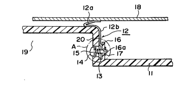
Figs. 2a and 2b show a power supply connector assembly
which is a second embodiment according to the present
invention and which corresponds to the conventional device
shown in and explained with reference to Fig. 7. Generally
it is to be understood that the drawings only show only one
of the members (or parts) where such members are in a pair.
, 20 For example, only a hole 21 is seen in Fig. 2a but there
,Y are a pair of holes 21, 22 as seen in Fig. 3.
~, The connector assembly shown in Figs. 2a and 2b is
adapted to be incorporated in an electronic device having a
battery pack holding section 19 defined by a wall of a
housing case 11 for holding a battery pack 37. There is a
s
-!
S
i
,', :
j 2~217~
74002-1
prlnted clrcult board 18 which carrles at lts undersurface a
contact pattern 3. The sprlng connector 12 lncludes a termlnal
pln 14 havlng a head electrlcally connectable to the battery pack
37 (see Flgs. 3 and 4c), a coll sprlng 15 carrled by the termlnal
pln 14, a termlnal leaf sprlng 12b havlng a bent extended portlon : -
formlng a sprlng contact 12a and havlng a base portlon engaglng
wlth sald termlnal pln 14, and a mountlng rlb 16 standlng up from
the houslng case 11. Each of the wall 20, the termlnal leaf
sprlng 12b and the mountlng rlb 16 has a hole through whlch the
termlnal pln 14 extends and the mountlng rlb 16 holds the termlnal
leaf sprlng 12b wlth the coll sprlng 15 presslng the termlnal leaf
sprlng 12b agalnst the mountlng rlb 16. Thus, the sprlng contact
12a formed at the tlp of the extended bent portlon of the termlnal
leaf spring 12b ls ln constant electrlc contact wlth the contact
pattern 3 on the prlnted clrcult board 18.
The sprlng connector 12 lncludes a retalner rlng or E-
rlng 17 whlch engages wlth the terminal pln 14 at lts end portlon -
pro~ectlng out from the mountlng rlb 16. Thls E-rlng 17 serves as
a stopper and the termlnal pln 14 and the termlnal leaf sprlng 12b
are held to the mountlng rlb 16. The houslng case 11 lncludes a
groove 13 deflned between the wall and the mountlng rlb 16 for
recelvlng the termlnal leaf sprlng 12b ln posltlon. The terminal
leaf sprlng 12b
- .
. :. ~. :
, ,. ~.
''';' ' ' .
~` 2~2~7~
1 directly rests on the inner surface of the wall of the case
11 .
The terminal pin 14 and the coil spring 15 in the
arrangement according to this embodiment correspond to and
similarly arranged as the terminal pin 14 and the coil
spring 15 in the conventional arrangement shown in Fig. 6.
,,
However, the terminal leaf spring 12b in this embodiment
replaces the sub-circuit plate 31 and the wire 36 shown in
the conventional arrangement of Fig. 6. The extended
: 10 portion 12a of the leaf spring 12b is bent in a ~-shape for
forming the spring contact.
Fig. 3 shows how the power supply connector assembly
having the configuration explained with reference to Fig.
2a is assembled when used in an electronic device.
The electronic device exemplified herein comprises a
housing 11 which has a battery pack holding-section 19 for
z ~ holding a battery pack 37 and a printed circuit board 18 -
3 wh'zch is pressed against and fixed by appropriate means
~3Z such as screws to the housing case 11. The printed circuit
board 18 has, on i~s back surface, printed circuits or
contact patterns and carries, on its front side, such means
as a liquid crystal display and a keyboard (see Fig. 4b).
Spring connector 12 stands upward from the housing case 11.
The contact patterns or pattern terminals on the printed
circuit board 18 are in contact with the spring contacts
.
- 1 1 - ~ '
.'r '.' ' ' ' ' ' ' ' ' ' '.. '.' :' . : , . . . .
20217~
1 12a of the spring connector 12 with the extended bent
~` portion of the terminal leaf spring 12b being pressed
against the pattern terminals on the printed circuit board
:.~ 18. The constant compression is due to the spring force of
~.
the terminal leaf spring 12b and this ensures stable and
constant electrical contact between the printed circuit
; board 18 and the terminal leaf spring 12b and, in turn,
between the terminal pin 14 and the printed circuit board
., 18.
~ 10 According to this second embodiment, the power supply
connection terminal ~or connecting the battery pack 37 to
the printed circuit board 18 in a device such as a portable
wireless telephone device includes the terminal pin 14, the
~ coil spring 15 and the terminal leaf spring 12b with the
:~ 15 arrangement wherein the extended bent portion of the termi-
nal leaf 12b spring forming the spring contact 12a is
directly in press-contact against the contact pattern on
the printed circuit board 18. The corresponding conven-
tional connector assembly configuration described requires
the sub-base plate 31 for the power supply terminal, and
, the sub-base plate 31 and the main circuit plate 18 are
' connected with each other by the wire 36. The connector
3~ assembly according to this embodiment is simpler as it does
.~ not require such members as the sub-base plate 31 and the
wire 36. With this configuration, the connection with
- 12 -
.'' ~
. .
. 2~217~4
1 printed circuit board 18 can be easily established and the
assembly can be fabricated and maintained in a simpler
manner than in the corresponding conventional assembly as
shown in Fig. 7.
,,
Figs. 4a, 4b and 4c show an example wherein the power
supply connector assembly as shown in Figs. la, lb and that
shown in Figs. 2a, 2b are incorporated in a wireless tele-
phone device. Fig. 4a illustrates a front cover 41a of the
telephone device, shown downside up, which includes spring
~ 10 connectors 2, an earpiece 42, a speaker 43 and a mouthpiece
¦ microphone 44. The front cover 41a also includes a flexi-
ble printed circuit board 45 which is in contact with the
spring connector 2. Fig. 4b shows a printed circuit board
18 which includes the necessary number of contact patterns
for connections with the related spring connectors and
other circuit-related parts such as a liquid crystal dis-
play 46 and a keyboard 47. Fig. 4c shows a rear case 41b
(which corresponds to the housing case 11 in Figs. 2a and
3), from which it is seen that the device incorporates
therein both the types of spring connectors, one being the
plunger type spring connectors 2 and the other being the
leaf spring type spring connector 12. The plunger type
spring connectors 2 in the front cover 41a and those in the
rear case 41b sandwich the printed circuit board 18 and
j~ 25 establish electric contacts with the front and the rear
- 13 -
1: .
2~217~
1 surfaces of the circuit board 18 while the leaf spring type
spring connector 12 establishes electric connection from
:
the battery pack 37 to the printed circuit board 18.
. While the invention has been described in its pre-
ferred embodiments, it is to be understood that the words
, which have been used are words of description rather than
; limitation and that changes within the purview of the
appended claims may be made without departing from the true
scope and spirit of the invention in its broader aspect.
.~
^` 10
~,,,
.. ':
.~ ~
~,
`~' 20
, ;,
., .
~'
,. . .
.. .. .
.i , " . , , ", , ", , , " " , , , " ", ,~,~ ", ~, " " ~ , ", ~, ,, ~ , ,,, , , ,~ ,, :: ~ ,