Note: Descriptions are shown in the official language in which they were submitted.
2~2~8~3
AE-327 PATENT
ELECTRICAL FILTER CONNECTOR
1 FIELD OF T~E I~E~TION:
T~ present i~ention relates to electrical connectors and
more particularly to an electrical filter connector for
reducing electromagnetic interference and for providing higher
voltage capability.
BACKGROUND OF THE INVENTION-
_
Electrical filter connectors for filtering electronic
- equipment from e~ectromagnetic interference (EMI) and radio
frequency interference (RFI) are well known in the electrical
connector art. Such electrical filter connectors may utilize
monolithic chip capacitors as shown in U.S. Patent 4,500,159
~Hogan et al.), thick film capacitors as shown in U.S. Patent
r 4,791,391 (Linell et al.) or ferrite materials as shown in U.S.
Patent 4,761,147 (Gauthier), to identify several known
examples.
While there are many applications for electrical filter
connectors, increasing need has developed for use of such
filter connec,tors in telecommunications and data-processing
systems. In such systems, in addition to protecting the
electronic e~uipment against EMI and RFI interference, there
is also need to protect the equipment against electrical power
! surges that result from electro-static discharges caused, for
example, by a lightning strike. While various of the known ~`
filtering devices as identified hereinabove, have been used to
provide such filtering capability, size and cost are placing
further demands upon the design of such electrical filter
connectors. For example, enhanced filtering effectiveness can ;~
- be achieved by smaller size devices due to a short conduction -i
path from the capacitors to the ground plane on system circuit
boards. Such size demands for reduced electronic devices,
including connectors, presents a difficult problem in providing
a filtering device capable especially of meeting the higher
;
2~2l~a~
l voltages experienced in power surge conditions without
bre~o~n ~f the filtering device. One known techni~ue of
ihcreasin~ ~he ~ielectri~ s~rength of the filtered connector
is to cover the capacitors with die~ectric oil. Such a
technique disad~ntageously re~lires some physical constraint
for containing the oil and in some instances, depending upon
the type of oil used, is hazardous. Accordingly, there is
present need for an electrical filter connector that includes
filtering devices enabling the connector to be constructed in
the desired size and to meet the higher voltage demands
occasioned by power surges as well as to be cost effective in
its construction for manufacture.
SUMMARY OF THE INVENTION:
. .
It is an object of the present invention to provide an
improved electrical filter connector.
It is a further object of the present invention to provide
an improved electrical filter connector having a capacitor sub-
assembly with enhanced dielectric strength.
In accordance with the invention, the improved electrical
ilter connector is of the type including an insulative housing
supporting a plurality of electrical contacts with a metal
shell supported by the housing substantially surrounding the
contacts. A resilient ground spring is provided in electrical
engagement with the metal shell, the ground spring having a
resilient portion projecting from the connector for resilient
engagement with a ground trace on a system circuit board.
Included are a plurality of capacitors, each having a pair of
spaced terminations, a first termination of each capacitor
being in electrical engage~ent with respective electrical
contacts and a second termination of each capacitor being in
electrical engagement with the ground spring. The improvement
of the connector comprises a capacitor sub-assembly comprising
an insulative substrate, the plurality of capacitors and the
ground spring. The capacitors are supported by ~he substrate
2~2~3
-3-
1 in a manner wherein the first capacitor terminations are
electrica~ n~i~idu~tly co~nected to the respective contacts
and the seco~d ~a~acit~r te~inations are electrically
connected to the ground spring. The capacitors are of the type
wherein a dielectric surface extends between the first and
second terminations and in the sub-assembly a curable
dielectric material is disposed on the dielectric surface
between each of the f~rst and second terminations.
In accordance with another embodiment of the invention,
the improvement of the electrical filter connector includes a
- capacitor s~b-assembly wherein the first capacitor terminations
are electrically individually connected to the respective
contacts by conductive elements on the substrate and plural of
the second capacitor terminations are electrically connected
in common by a conductive member on the substrate. The ground
~ spring is further electrically connected to the conductive
; member such that the plural second capacitor terminations may
be electrically commonly connected to the ground trace on the
system circuit board.
In a further embodiment of the invention, the electrical
filter connect,or is of the type wherein the electrical contacts
each have a compliant terminal ~or resilient electrical
' engagement with openings in the system circuit board. The
connector improvement comprises the insulative housing formed
of a base and an insert wherein the electrical contacts are
captively retained thereby. As such, during insertion of the
~ compliant terminals of the electrical contacts into the
; openings of the system circuit board, an insertion force may
be applied to the insulative housing whereby such insertion
force is transferred to the electrical contacts for insertion
of such contacts into the system circuit board.
:
BRIEF DESCRIPTIO~ OF THE DRAWINGS:
Figure } is a side elevation view of an electrical filter
3~ connector in accordance with a preferred embodiment of the
invention, partially sectioned to reveal internal construction
details thereof.
2~2~
,~
- 1 Figure 2 is a cross-sectional view o~ the electrical
~ er con~ector Q~ Figure ~ as se2n along viewing lines II -
II o~ g~re ~, wit~ ~e further s~owing of a system circuit
board to whi~h the electrical filter connector is connected.
Figure 3 is a bottom plan view of a capacitor sub-assembly
in accordance with the improvement o~ the electrical filter
connector of Figure 1.
Figure 4 is a side elevation view of the capacitor sub-
assembly of Figure 3.
Figure 5 is an enlarged side view of the ground spring of
the capacitor sub-assembly in accordance with a preferred
embodiment thereof, showing in phantom a particular ground
spring construction.
Figure 6 is a plan view showing a pair of electrical
~ 15 contacts of the improved electrical filter connector showing
¦ in phantom a carrier strip used during the manufacture thereo~.
.1
¦ DETAILED DESCRIPTION OF THE PREFERRED EMBODIMENTS:
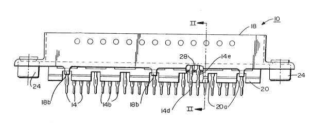
¦ Referring now to the drawings, there is shown in Figures
1 and 2 an electrical filter connector 10 in accordance with
a preferred embodiment of the invention. The connector 10
l includes an elongate insulative housing 12 supporting in two
I longitudinally disposed transversely spaced rows a plurality
of electrical contacts 14. Each of the contacts 14 comprises
an upper resilient spring section 14a for electrical engagement
with contacts of a complementary electrical connector and pin
sections 14b for electrical engagement with conductive circuits
on a system circuit board 16, as will be descri~ed more ~ully
hereinafter.
A metal shell 18 is s~pported by the housing 12, the shell
having walls substantially surrounding the electrical contacts
in a manner t~ provide E~I and RFI protection. A resilient
ground spring 2~ is supported by the connectcr housing 12 along
each o~ the longitudinal edges thereof, the ground spring being
35 in electrical engagement with the metal shell 18. As
1 illustrated in Figure 1, the ground spring 20 has a series of
cutaway portions 20a which provide enhanced resiliency o~ the
sprin~ 20. Each of the ground springs 20 is adapted, as will
be ~r~er des~ hereinafter, to be in electrical
connectio~ wi~h capacitors 22 provided in the electrical
connector for electronic interference filtering. Upon
attachment of the electrical ~ilter connector 10 to the system
circuit board 16, the metal shell 18 thereof is secured to the
board 16 with fasteners inserted through bushings 24 disposed
at the longitudinal ends of the shell 18.
By further reference now to Figures 3 and 4, an
improvement of the electrical filter connector in accordance
with a preferred embodiment of the invention is described. As
shown therein, a capacitor sub-assembly 26 comprises an
elongate insulative substrate 28 which supports thereon the
resilient ground springs 20 and a plurality of capacitors 22.
The substrate 28 preferably comprises a printed circuit board.
The printed circuit board 28 includes therethrough a plurality
of openings 30, each of which has its interior walls and an
adjacent surface of the printed circuit board 28 metallized
with conductive material by ~nown conventional techniques. The
metallized surfaces of the openings 30 and the surrounding
I surface areas, provide conductive elements 32 for electrical
!` connection to the electrical contacts and capacitors, as will
be described. The openings 30 are disposed in two
longitudinally extending transversely spaced rows in a pattern
, the same as the electrical contacts such that the pin sections
; 14b thereof may be received therethrough.
Still re~erring to Figures 3 and 4, the printed circuit
board 28 further includes along each of its longitudinal edges
a metallized strip 34 extendin~ along the respective edges for
nearly the length of the printed circuit board 28. The
metallized strips 34 each provide a conductive member for
attachment to the capacitors 22 and to the ground springs 20.
In the preferred embodiment, the capacitors 22 are discrete,
2~2~
--6--
1 monolithic, multilayer chip capacitors. As is known, each such
capacitor 22 is ~ormed ~eneral~y in parallelepiped
configuration ~aving a pair of conductive terminations 22a and
22b disposed externally on a dielectric bod~ 22c with a
diele~tric surface extending between the terminations 22a and
22b as further shown in Figure 2. The metallized portions 32
and the metallized strips 34 in a particular form of the
printed circuit board 28 are provided identically on both major
surfaces of the substrate 28.
With further reference now to Figure 5, the details of the
ground spring 20 are descrihed. The spring 20 is formed of a
resilient conductive material, such as phosphor bronze and
, includes an angularly formed portion 20a which is adapted to
! obliquely engage the upper surface o~ the system circuit board
16. The upper portion of the spring is formed generall~ in the
shape of a sideways U-shaped cup 20b for attachment to the side
~; edges of the printed circuit board 28. The cup 20b includes
extents 20c and 20d that are adapted to lie adjacent opposed
sur~aces of the printed circuit board 28 and adjacent the
metallized s~rips 34. Extent 20c, as illustrated in phantom
in Figure 5, may be formed to project inwardly into such cup
I so as to provide a resilient attachment feature whereby the
i~ ground spring may be temporarily held on the edge of the
printed circuit board 28 prior to permanent securement thereto.
Turning now again to Figures 3 and 4 as well as to Figure
2, the assembly of the capacitor sub-assembly 26 and its final
, construction are described. The plurality of capacitors 22 are
each suitably held in alignment with the respective apertures
30 with the first set of terminations 22a in contact with
respective metallized portions 32 and with the second set of
terminations 22b in each row being in contact with a respective
metallized strip 34. The capacitors are soldered thereto such
that terminations 22a are individually electrically connected
to the metallized openings 30 and the terminations 22b are
electrically attached in common in each row to a metallized
2~2~3
1 strip 34. The ground springs are temporarily heid onto the
respective edges o~ the printed circuit board 28 by the cup
portion 2~. r~he extents 20c and 20d of the springs 20 are
then s~l~ered to the ~etallized strips 34, thereby electrically
connecting each of the ground springs 20 to a row of capacitor
terminations 22b. The c~pacitors 22 and the ground springs 20
may be soldered in a common operation.
Subsequent to the soldering of the capacitors 22 and the
ground springs 20 to the board 28, in accordance with the
invention, a quantity of dielectric material is applied onto
the capacitors. As illustrated in Figures 2, 3 and 4, a
dielectric material 36 is disposed on the dielectric surface
of each of the capacitors between the terminations 22a and 22b.
It has been found that the application of the additional
dielectric material which places a high dielectric medium
between the terminations of the capacitor, permitting a higher
voltage capability whereby the electrical connector may
withstand certain power surges. For example, size constraints
o~ the connector likewise place constraints on the capacitor
sizes that may be utilized. As such, in order to meet such
size constrai~ts, conventional capacitors may be able to meet
power surges at voltages up to 500 volts RMS due to the
breakdown of the air gap between the capacitor terminations.
Utilization of additional dielectric material increases the
dielectric strength of the medium between capacitor
terminations thereby increasing the capability of the connector
to withstand power surges at voltages up to 1,250 volts RMS,
or greater.
In accordanoe with the preferred technique of applying the
dielectxi~ material to the capacitor sub-assembly, the material
is applied subse~uent to the soldering of the capacitors 22 to
the printed circuit board 28. Upon attachment thereto, there
exists between the printed circuit board 28 and the dielectric
body 22c of the capacitors 22 a space 38 which would normally
be filled with air. A series of apertures 40 is formed through
2~2~
1 the printed circuit board 28 in registry with each of the
capacit~s ~2~ ~p~rtures 40 communicating with the space 38.
The dielectric Materi~l 36, whic:h is in fluid curable form, is
inserted through the apertures 40 into the spaces 38 and around
the side surfaces of each of the capacitors 22. As used
herein, the term "curable" is intended to mean a viscous
material in fluid form that, with time, cures to a firm state
without the need for physical constraints. Preferably, the
curable dielectric material is applied under a suitable
pressure. Further, an additional coating of curable dielectric
material may be applied, as depicted in Figure 3,
longitudinally continuously along the capacitors 22 on the
surface of the capacitors opposite the spaces 38. In the
preferred arrangement, the curable dielectric material is a
material sold under the trade name CHIP BONDER purchased from
` Loctite Corporation, Connecticut. This material is normally
used as an insulative adhesive to hold components in place for
soldering and has been found to have the suitable dielectric
properties for enhancing the die}ectric capability of the
electrical filter connector hereof as well as having the fluid
` properties for ease of application and curing. It should be
I appreciated that other techniques for applying the curable
dielectric material may also be utilized within the
contemplated scope of the invention. For example, a common
aperture in ref~istry with plural of the capacitors and
communicating with plural spaces may be used. Also, the
` curable dielectric material 36 may bé applied to the surface
of the substrate 28 prior to soldering the capacitors thereto.
Whatever the application technif~ue, the application of the
dielectric material, preferab~f~ully perimetrically around the
dielectric body 22c of eàch capacitor enh~nces the dielectric
capability.
Referring now to Figures 2 and 6, the construction of the
improved electrical filter connector is described. As
illustrated in Fi~ure 6f the electrical contacts, two of which
2~2~
:.,
1 are shown attached t~ ~ removable carrier strip 42 during the
preferred manufacturing operation, comprise a spring section
14a, a pin section 14b and a support section 14c. In the
preferred form of the electrical contacts, the pin section
comprises tw~ compliant sections 14d and 14e. As is known in
the electrical connector art, a compliant section is of the
type that is used to make resilient electrical engagement to
metallized w~lls of openings in a printed circuit board,
wherein the compliant section includes tines or arm portions
10 ~ that are e~astically de~ormable upon insertion of the compliant
- section into such metallized openings.
Upon withdrawal of the compliant sections from the
metallized openings, the board 28 may be used. In the
preferred construction of the electrical contact of the subject
; 15 connector, the compliant section 14d serves as a compliant
terminal for insertion of the connector into a system circuit
¦ board, such as board 16. Compliant section 14e is utilized in
the subject connector in the preferred arrangement, to make
'¦ electrical connection to the capacitors in the capacitor sub-
assembly as will be set ~orth.
In the preferred construction of the electrical filter
connector, the insulative housing 12 comprises a base 44 and
! an insert ~6. Captively retained between the base and theinsert is the support section 14c which is defined particularly
by a shoulder 14f which includes a portion projecting from each
of the contacts substantially transversely to the pin sections
thereof. The metal shell 18 is attached to and supported by
the base 44.
The capacitor sub-assembly 26 is attached in the
electrical filter connector 10 at its underside. The pin
sections 14b o~ each of the electrical contacts are inserted
through the metallize~ openings 30 of the printed circuit board
28 such that the compliant sections 14e are disposed in press
fit electrical engagement with the metallized portions 32 of
the openin~s 30. Tabs 18b on the metal shell 18 are bent
2~2~8~3
--10--
1 around the marginal edges of the capacitor sub-assembly 26 to
engage the ground springs 20, thus causing electrical
co~L~c~o~ ~mo~s~ ~e metal shel~ 18, ground sprin~s 20 and
capacitbr te~inations 22b.
In use, as shown in Figure 2, the electrical connector 10
of the subject invention is attached to the system circuit
board 16 ~y inserting the compliant terminals 14d into
metallized openings 16a of the system circuit board 16 such
that the compliant terminals l~d are disposed in a press fit
engagement therewith. During such insertion, a force, such as
- force F, as schematically shown in Fig. 2, may be applied to
the base 44 of the housing 12, either directly or through a
dust cover tnot shown). Force F is transferred to the shoulder
portion 14f and thus to the pin sections 14b for attachment to
the circuit board 16. During insertion of the contacts 14 into
the system board 16, the ground springs 20 engage conductive
traces 16b formed on the system board 16, and such ground
springs 20 resiliently deform to provide a pressure engagemPnt
with the traces 16b. In use, traces 16b may be electrically
connected to a ground potential, thereby attaching to ground
through the ground spring 20 the capacitor terminations 22b and
the metal shell 18. Terminations 22a are electrically
'i connected through respective contacts 14b to electrical circuit
I devices that may be connected to the metallized portions 16a
¦ 25 on the system circuit board 16.
Having described the preferred embodiment of the
invention, it should now be appreciated that variations may be
I made thereto without departing from the contemplated scope of
the invention. For example, it should be understood that while
the pre~erred contact structure comprises two compliant
sections 14d and 14e the contact pin sections may be formed
with neither of these co~pliant sections but rat~er with a
straight-through pin which may be soldered to both the
metallized portions 32 on the sub-assembly 26 and to the
metal-ized portions 16a on the system board 16. Further,
another variation may include the use of a single compliant
2~2~
1 section, such as 14e which may be press fit into the metallized
ope~in~s 32 in t.he capacitsr s~b-assembly with the contact
terminals c~pri~ing a ~raigh~-through pin for ultimate
soldering to the metallized openings 16a in the system circuit
board 16. Accordingly, the preferred embodiments described
herein are intended in an illustrative rather than a limiting
sense. The true scope of the invention is set forth in the
claims appended hereto.
,
, 15
I
,1 :
. ;
.