Some of the information on this Web page has been provided by external sources. The Government of Canada is not responsible for the accuracy, reliability or currency of the information supplied by external sources. Users wishing to rely upon this information should consult directly with the source of the information. Content provided by external sources is not subject to official languages, privacy and accessibility requirements.
Any discrepancies in the text and image of the Claims and Abstract are due to differing posting times. Text of the Claims and Abstract are posted:
| (12) Patent Application: | (11) CA 2021826 |
|---|---|
| (54) English Title: | DELAY LOGIC FOR PREVENTING CPU LOCKOUT FROM BUS OWNERSHIP |
| (54) French Title: | CIRCUIT DE RETARDEMENT COMMANDE PAR UN CIRCUIT LOGIQUE POUR EMPECHER L'UNITE CENTRALE DE PERDRE LE CONTROLE DU BUS |
| Status: | Deemed Abandoned and Beyond the Period of Reinstatement - Pending Response to Notice of Disregarded Communication |
| (51) International Patent Classification (IPC): |
|
|---|---|
| (72) Inventors : |
|
| (73) Owners : |
|
| (71) Applicants : |
|
| (74) Agent: | |
| (74) Associate agent: | |
| (45) Issued: | |
| (22) Filed Date: | 1990-07-24 |
| (41) Open to Public Inspection: | 1991-04-24 |
| Examination requested: | 1994-10-31 |
| Availability of licence: | N/A |
| Dedicated to the Public: | N/A |
| (25) Language of filing: | English |
| Patent Cooperation Treaty (PCT): | No |
|---|
| (30) Application Priority Data: | ||||||
|---|---|---|---|---|---|---|
|
BC9-89-044
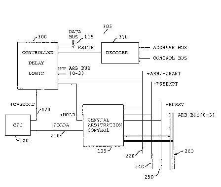
ABSTRACT
A logic controlled delay circuit is connected into the
arbitration logic of a computer system of the type having
a main data bus which is subject to control by multiple
masters. The delay is so programmed that the default
master, which is the main processor (CPU) for the system
and is assigned the residual or default priority, is
assured a predefined portion of the time available on the
bus. By so inserting and controlling the delay that the
"hold" signal to the CPU is delayed whenever the CPU is
granted access to the bus, other devices, are unable to
seize the bus until the delay has ended at which time the
CPU is triggered by the delayed signal to respond with an
acknowledge which serves to permit arbitration to begin.
By this technique a standard microprocessor such as an
Intel 80386 can operate in such an architecture without
being preempted from the bus by the higher priority
devices to an extent that system operation deteriorates.
Note: Claims are shown in the official language in which they were submitted.
Note: Descriptions are shown in the official language in which they were submitted.
2024-08-01:As part of the Next Generation Patents (NGP) transition, the Canadian Patents Database (CPD) now contains a more detailed Event History, which replicates the Event Log of our new back-office solution.
Please note that "Inactive:" events refers to events no longer in use in our new back-office solution.
For a clearer understanding of the status of the application/patent presented on this page, the site Disclaimer , as well as the definitions for Patent , Event History , Maintenance Fee and Payment History should be consulted.
| Description | Date |
|---|---|
| Inactive: Dead - No reply to s.30(2) Rules requisition | 2001-10-01 |
| Application Not Reinstated by Deadline | 2001-10-01 |
| Deemed Abandoned - Failure to Respond to Maintenance Fee Notice | 2001-07-24 |
| Inactive: Abandoned - No reply to s.30(2) Rules requisition | 2000-10-02 |
| Inactive: Status info is complete as of Log entry date | 2000-09-11 |
| Inactive: Application prosecuted on TS as of Log entry date | 2000-09-11 |
| Inactive: S.30(2) Rules - Examiner requisition | 2000-06-01 |
| Inactive: Reversal of dead status | 1999-07-05 |
| Inactive: Delete abandonment | 1999-07-05 |
| Inactive: Dead - No reply to s.30(2) Rules requisition | 1998-08-21 |
| Inactive: Office letter | 1997-12-02 |
| Inactive: Office letter | 1997-12-02 |
| Inactive: Abandoned - No reply to s.30(2) Rules requisition | 1997-08-21 |
| Inactive: S.30(2) Rules - Examiner requisition | 1997-02-21 |
| All Requirements for Examination Determined Compliant | 1994-10-31 |
| Request for Examination Requirements Determined Compliant | 1994-10-31 |
| Application Published (Open to Public Inspection) | 1991-04-24 |
| Abandonment Date | Reason | Reinstatement Date |
|---|---|---|
| 2001-07-24 |
The last payment was received on 2000-05-25
Note : If the full payment has not been received on or before the date indicated, a further fee may be required which may be one of the following
Patent fees are adjusted on the 1st of January every year. The amounts above are the current amounts if received by December 31 of the current year.
Please refer to the CIPO
Patent Fees
web page to see all current fee amounts.
| Fee Type | Anniversary Year | Due Date | Paid Date |
|---|---|---|---|
| MF (application, 7th anniv.) - standard | 07 | 1997-07-24 | 1997-05-28 |
| MF (application, 8th anniv.) - standard | 08 | 1998-07-24 | 1998-05-14 |
| MF (application, 9th anniv.) - standard | 09 | 1999-07-26 | 1999-05-17 |
| MF (application, 10th anniv.) - standard | 10 | 2000-07-24 | 2000-05-25 |
Note: Records showing the ownership history in alphabetical order.
| Current Owners on Record |
|---|
| INTERNATIONAL BUSINESS MACHINES CORPORATION |
| Past Owners on Record |
|---|
| DARRYL EDMOND JUDICE |

